AT24C02简介
- 格式:doc
- 大小:123.50 KB
- 文档页数:3
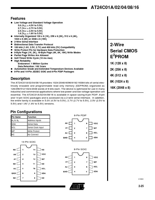
Features•Low Voltage and Standard Voltage Operation5.0 (V CC = 4.5V to 5.5V)2.7 (V CC = 2.7V to 5.5V)2.5 (V CC = 2.5V to 5.5V)1.8 (V CC = 1.8V to 5.5V)•Internally Organized 128 x 8 (1K), 256 x 8 (2K), 512 x 8 (4K),1024 x 8 (8K) or 2048 x 8 (16K)•2-Wire Serial Interface•Bidirectional Data Transfer Protocol•100 kHz (1.8V, 2.5V, 2.7V) and 400 kHz (5V) Compatibility •Write Protect Pin for Hardware Data Protection•8-Byte Page (1K, 2K), 16-Byte Page (4K, 8K, 16K) Write Modes •Partial Page Writes Are Allowed •Self-Timed Write Cycle (10 ms max)•High ReliabilityEndurance: 1 Million Cycles Data Retention: 100 Years•Automotive Grade and Extended Temperature Devices Available •8-Pin and 14-Pin JEDEC SOIC and 8-Pin PDIP PackagesDescriptionThe AT24C01A/02/04/08/16 provides 1024/2048/4096/8192/16384 bits of serial elec-trically erasable and programmable read only memory (EEPROM) organized as 128/256/512/1024/2048 words of 8 bits each. The device is optimized for use in many industrial and commercial applications where low power and low voltage operation are essential. The AT24C01A/02/04/08/16 is available in space saving 8-pin PDIP, 8-pin and 14-pin SOIC packages and is accessed via a 2-wire serial interface. In addition,the entire family is available in 5.0V (4.5V to 5.5V), 2.7V (2.7V to 5.5V), 2.5V (2.5V to5.5V) and 1.8V (1.8V to 5.5V) versions.Pin Configurations8-Pin PDIP8-Pin SOIC14-Pin SOICAT24C01A/02/04/08/16Block Diagram*NOTICE: Stresses beyond those listed under “Absolute Maxi-mum Ratings” may cause permanent damage to the device.This is a stress rating only and functional operation of thedevice at these or any other conditions beyond those indi-cated in the operational sections of this specification is notimplied. Exposure to absolute maximum rating conditionsfor extended periods may affect device reliability. Absolute Maximum Ratings*Pin DescriptionSERIAL CLOCK (SCL): The SCL input is used to positiveedge clock data into each E2PROM device and negativeedge clock data out of each device.SERIAL DATA (SDA): The SDA pin is bidirectional for se-rial data transfer. This pin is open-drain driven and may bewire-ORed with any number of other open-drain or opencollector devices.DEVICE/PAGE ADDRESSES (A2, A1, A0): The A2, A1and A0 pins are device address inputs that are hard wiredfor the AT24C01A and the AT24C02. As many as eight1K/2K devices may be addressed on a single bus system(device addressing is discussed in detail under the DeviceAddressing section).The AT24C04 uses the A2 and A1 inputs for hard wireaddressing and a total of four 4K devices may be ad-dressed on a single bus system. The A0 pin is a no con-nect.The AT24C08 only uses the A2 input for hardwire ad-dressing and a total of two 8K devices may be addressedon a single bus system. The A0 and A1 pins are no con-nects.The AT24C16 does not use the device address pins whichlimits the number of devices on a single bus to one. TheA0, A1 and A2 pins are no connects.(continued)Applicable over recommended operating range from: T AI = -40°C to +85°C, V CC = +1.8V to +5.5V, T AC = 0°C to +70°C,Note:1.V IL min and V IH max are reference only and are not tested.DC CharacteristicsWRITE PROTECT (WP): The AT24C01A/02/04/16 has a Write Protect pin that provides hardware data protection.The Write Protect pin allows normal read/write operations when connected to ground (GND). When the Write Protectpin is connected to V CC , the write protection feature is en-abled and operates as shown in the following table.Pin Description (Continued)Memory OrganizationAT24C01A, 1K SERIAL E 2PROM: Internally organized with 128 pages of 1-byte each, the 1K requires a 7 bit data word address for random word addressing.AT24C02, 2K SERIAL E 2PROM: Internally organized with 256 pages of 1-byte each, the 2K requires an 8 bit data word address for random word addressing.AT24C04, 4K SERIAL E 2PROM: The 4K is internally or-ganized with 256 pages of 2-bytes each. Random word addressing requires a 9 bit data word address.AT24C08, 8K SERIAL E 2PROM:The 8K is internally or-ganized with 4 blocks of 256 pages of 4-bytes each. Ran-dom word addressing requires a 10 bit data word address.AT24C16, 16K SERIAL E 2PROM: The 16K is internally organized with 8 blocks of 256 pages of 8-bytes each.Random word addressing requires an 11 bit data word ad-dress.Pin Capacitance (1)Note:1. This parameter is characterized and is not 100% tested.AT24C01A/02/04/08/16Note:1. This parameter is characterized and is not 100% tested.Applicable over recommended operating range from T A = -40°C to +85°C, V CC = +1.8V to +5.5V, CL = 1 TTL Gate and100 pF (unless otherwise noted).AC CharacteristicsDevice OperationCLOCK and DATA TRANSITIONS: The SDA pin is nor-mally pulled high with an external device. Data on the SDA pin may change only during SCL low time periods (refer to Data Validity timing diagram). Data changes during SCL high periods will indicate a start or stop condition as de-fined below.START CONDITION: A high-to-low transition of SDA with SCL high is a start condition which must precede any other command (refer to Start and Stop Definition timing diagram).STOP CONDITION: A low-to-high transition of SDA with SCL high is a stop condition. After a read sequence, the stop command will place the E 2PROM in a standby power mode (refer to Start and Stop Definition timing diagram).ACKNOWLEDGE: All addresses and data words are se-rially transmitted to and from the E 2PROM in 8 bit words.The E 2PROM sends a zero to acknowledge that it has re-ceived each word. This happens during the ninth clock cy-cle.STANDBY MODE: The AT24C01A/02/04/08/16 features a low power standby mode which is enabled: (a) upon power-up and (b) after the receipt of the STOP bit and thecompletion of any internal operations.Bus Timing SCL: Serial ClockSDA: Serial Data I/OWrite Cycle Timing SCL: Serial Clock SDA: Serial Data I/ONote: 1.The write cycle time t WR is the time from a valid stop condition of a write sequence to the end of the internal clear/write cycle.AT24C01A/02/04/08/16Data ValidityStart and Stop DefinitionOutput AcknowledgeDevice AddressingThe 1K, 2K, 4K, 8K and 16K E2PROM devices all require an 8 bit device address word following a start condition to enable the chip for a read or write operation (refer to Fig-ure 1).The device address word consists of a mandatory one, zero sequence for the first four most significant bits as shown. This is common to all the E2PROM devices.The next 3 bits are the A2, A1 and A0 device address bits for the 1K/2K E2PROM. These 3 bits must compare to their corresponding hard-wired input pins.The 4K E2PROM only uses the A2 and A1 device address bits with the third bit being a memory page address bit. The two device address bits must compare to their corre-sponding hard-wired input pins. The A0 pin is no connect. The 8K E2PROM only uses the A2 device address bit with the next 2 bits being for memory page addressing. The A2 bit must compare to its corresponding hard-wired input pin. The A1 and A0 pins are no connect.The 16K does not use any device address bits but instead the 3 bits are used for memory page addressing. These page addressing bits on the 4K, 8K, and 16K devices should be considered the most significant bits of the data word address which follows. The A0, A1 and A2 pins are no connect.The eighth bit of the device address is the read/write op-eration select bit. A read operation is initiated if this bit is high and a write operation is initiated if this bit is low. Upon a compare of the device address, the E2PROM will output a zero. If a compare is not made, the chip will return to a standby state.Write OperationsBYTE WRITE: A write operation requires an 8 bit data word address following the device address word and ac-knowledgement. Upon receipt of this address, the E2PROM will again respond with a zero and then clock in the first 8 bit data word. Following receipt of the 8 bit data word, the E2PROM will output a zero and the addressing device, such as a microcontroller, must terminate the write sequence with a stop condition. At this time the E2PROM enters an internally-timed write cycle to the nonvolatile memory. All inputs are disabled during this write cycle and the E2PROM will not respond until the write is complete (refer to Figure 2).PAGE WRITE: The 1K/2K E2PROM is capable of an 8-byte page write, and the 4K, 8K and 16K devices are ca-pable of 16-byte page writes.A page write is initiated the same as a byte write, but the microcontroller does not send a stop condition after the first data word is clocked in. Instead, after the E2PROM acknowledges receipt of the first data word, the microcon-troller can transmit up to seven (1K/2K) or fifteen (4K, 8K, 16K) more data words. The E2PROM will respond with a zero after each data word received. The microcontroller must terminate the page write sequence with a stop con-dition (refer to Figure 3).The data word address lower three (1K/2K) or four (4K, 8K, 16K) bits are internally incremented following the re-ceipt of each data word. The higher data word address bits are not incremented, retaining the memory page row loca-tion. If more than eight (1K/2K) or sixteen (4K, 8K, 16K) data words are transmitted to the E2PROM, the data word address will “roll over” and previous data will be overwrit-ten.ACKNOWLEDGE POLLING: Once the internally-timed write cycle has started and the E2PROM inputs are dis-abled, acknowledge polling can be initiated. This involves sending a start condition followed by the device address word. The read/write bit is representative of the operation desired. Only if the internal write cycle has completed will the E2PROM respond with a zero allowing the read or write sequence to continue.Read OperationsRead operations are initiated the same way as write op-erations with the exception that the read/write select bit in the device address word is set to one. There are three read operations: current address read, random address read and sequential read.CURRENT ADDRESS READ: The internal data word ad-dress counter maintains the last address accessed during the last read or write operation, incremented by one. This address stays valid between operations as long as the chip power is maintained. The address “roll over” during read is from the last byte of the last memory page to the first byte of the first page. The address “roll over” during write is from the last byte of the current page to the first byte of the same page.Once the device address with the read/write select bit set to one is clocked in and acknowledged by the E2PROM, the current address data word is serially clocked out. The microcontroller does not respond with an input zero but does generate a following stop condition (refer to Figure 4).RANDOM READ: A random read requires a “dummy”byte write sequence to load in the data word address. Once the device address word and data word address are clocked in and acknowledged by the E2PROM, the micro-(continued) AT24C01A/02/04/08/16Figure 1.Device AddressFigure 2.Byte WriteFigure 3. Page Write(* = DON’T CARE bit for 1K)controller must generate another start condition. The mi-crocontroller now initiates a current address read by send-ing a device address with the read/write select bit high.The E 2PROM acknowledges the device address and seri-ally clocks out the data word. The microcontroller does not respond with a zero but does generate a following stop condition (refer to Figure 5).SEQUENTIAL READ: Sequential reads are initiated by either a current address read or a random address read.After the microcontroller receives a data word, it responds with an acknowledge. As long as the E 2PROM receives an acknowledge, it will continue to increment the data word address and serially clock out sequential data words.When the memory address limit is reached, the data word address will “roll over” and the sequential read will con-tinue. The sequential read operation is terminated when the microcontroller does not respond with a zero but does generate a following stop condition (refer to Figure 6).Read Operations(Continued)Figure 5. Random Read(*= DON’T CARE bit for 1K)Figure 4.Current Address ReadFigure 6. Sequential ReadAT24C01A/02/04/08/16Ordering InformationOrdering InformationOrdering Information。

EEPROM存储芯⽚24C021、24C02简介 24C02是⼀个2Kbit的串⾏EEPROM存储芯⽚,可存储256个字节数据。
⼯作电压范围为1.8V到6.0V,具有低功耗CMOS技术,⾃定时擦写周期,1000000次编程/擦除周期,可保存数据100年。
24C02有⼀个16字节的页写缓冲器和⼀个写保护功能。
通过I2C总线通讯读写芯⽚数据,通讯时钟频率可达400KHz。
可以通过存储IC的型号来计算芯⽚的存储容量是多⼤,⽐如24C02后⾯的02表⽰的是可存储2Kbit的数据,转换为字节的存储量为2*1024/8 = 256byte;有⽐如24C04后⾯的04表⽰的是可存储4Kbit的数据,转换为字节的储存量为2*1024/8 = 512byte;以此来类推其它型号的存储空间。
24C02的管脚图如下: VCC和VSS是芯⽚的电源和地,电压的⼯作范围为:+1.8V~+6.0V。
A0、A1、A2是IC的地址选择脚。
WP是写保护使能脚。
SCL是I2C通讯时钟引脚。
SDA是I2C通讯数据引脚。
2、24C02的设备地址和写保护功能 I2C主机在与24C02通讯时,需要发送⼀个设备地址进⾏寻址,在I2C总线上,每⼀个从机设备的地址都是唯⼀的。
24C02的设备地址包含两部分,第⼀部分是bit7~bit4是固定的“1010”,第⼆部分bit3~bit1位由A2、A1、A0组成。
主机在与24C02进⾏通讯时,除了发送设备地址还需要发送数据的读写⽅向位R/W,24C02的是设备地址与R/W位组成了⼀个字节的数据。
如下图: 上图列出了⼏个存储IC的设备地址与R/W位组成的字节。
由图中可以看到,存储IC地址的bit7~bit4位固定为“1010”;bit3~bit1位由A2、A1、A0引脚的电平状态决定,如果Ax接的是电源(⾼电平),那么Ax=1,如果Ax接的是地,那么Ax=0,即由A2、A1、A0可以组合成8种设备地址,也就是说在同⼀个I2C总线上可以同时挂载8个24C02芯⽚。


I2C详解I2C总线是PHLIPS公司推出的一种串行总线,是具备多主机系统所需的包括总线裁决和高低速器件同步功能的高性能串行总线。
I2C总线只有两根双向信号线:一根是数据线SDA,另一根是时钟线SCL。
I2C总线通过上拉电阻接正电源。
当总线空闲时,两根线均为高电平。
连到总线上的任一器件输出的低电平都将使总线的信号变低,即各器件的SDA及SCL都是线“与”关系。
在有些情况下,可能没接上拉电阻I2C也能正常通信,但是建议读者最好接上拉电阻。
本文最后将给出有接上拉电阻和没接两种情况下的I2C通信波形,可以明显的看出来,接了上拉电阻波形更漂亮,通信也更稳定。
本文将以24C02来详细讲解I2C 协议。
因为本文的重点是讲解I2C,所以这里只简单的介绍24C02,有关24C02的更为详细的资料,读者可以查阅其数据手册,在这里就其必需的部分进行简单的讲解。
一、 AT24C02简介AT24C02是美国ATMEL公司的低功耗CMOS串行EEPROM,它是内含256×8位(2K)存储空间,具有工作电压宽(2.5~5.5V)、擦写次数多(大于10000次)、写入速度快(小于10ms)等特点。
它的典型应用电路如图1:图1 AT24C02典型应用电路图1中AT24C02的1、2、3脚是三条地址线,用于确定芯片的硬件地址。
在本文都将其接地,表示其地址为000。
第5脚SDA为串行数据输入/输出,数据通过这条双向I2C总线串行传送,第6脚SCL为串行时钟输入线。
当用单片机I/O 口模拟I2C通信时,这两个引脚可以接任意的I/O口。
SDA和SCL都需要接一个上拉电阻,其阻值一般为4.7K~10K。
第7脚是写保护引脚,可以接IO口也可以直接接地,接地就不再具有保护功能。
这里将其直接接地。
二、 I2C总线的构成及信号类型I2C总线是由数据线SDA和时钟线SCL构成的串行总线,可发送和接收数据。
I2C总线进行数据传送时,时钟信号为高电平期间,数据线上的数据必须保持稳定,只有在时钟线上的信号为低电平期间,数据线上的高电平或低电平状态才允许变化。


存储芯片AT24C02
如图2-2为AT24C02的芯片引脚图。
图2-2 AT24C02的芯片引脚图
特点:低压和标准电压运行模式
– 2.7 (VCC = 2.7V to 5.5V)
– 1.8 (VCC = 1.8V to 5.5V)
内建128x8存储序列,2线制串行接口,双向数据传送协议,100kHz(1.8V,2.5V,2.7V) 和400kHz(5V)兼容,写同步时钟(最大10ms),高可靠性,极限:1M写时钟周期,数据保存:100年,不断推进的芯片等级扩大了设备的可用温度范围。
AT24C02提供电可擦除的串行1024位存储或可编程只读存储器(EEPROM)128字(8位/字)。
芯片在低压的工业与商业应用中进行了最优化。
设备操作:
CLOCK 和DATA变化:SDA管脚通常外部要拉高。
SDA管脚上的数据只能在SCL低期间改变。
数据在SCL高期间改变定义为一个开始或停止信号。
开始状态:在任何操作之前必须有一个开始信号----在SCL为高时SDA上产生一个下降沿。
停止状态: SCL为高时SDA产生一个上升沿是停止信号,停止信号后将停止所有通信。
在一个读的序列之后,停止信号将让EEPROM进入备用电源模式。
S P E C I F I C A T I O N24C02/24C04/24C08/24C16Version 1.0Two-wire Serial EEPROM2K bits (256 X 8) / 4K bits (512 X 8) / 8K bits (1024 X 8) / 16K bits (2048 X 8)▉FeaturesThe 24C02/24C04/24C08/24C16 provides 2048/4096/8192/16384 bits of serial electrically erasable and programmable read-only memory (EEPROM) organized as 256/512/1024/2048 words of 8 bits each. The device is optimized for use in many industrial and commercial applications wherelow-power and low-voltage operation are essential. The 24C02/24C04/24C08/24C16 is available in space-saving 8-lead PDIP, 8-lead SOP, and 8-lead TSSOP packages and is accessed via a two-wire serial interface.▉Pin ConfigurationTwo-wire Serial EEPROM2K bits (256 X 8) / 4K bits (512 X 8) / 8K bits (1024 X 8) / 16K bits (2048 X 8)▉Pin DescriptionsTwo-wire Serial EEPROM2K bits (256 X 8) / 4K bits (512 X 8) / 8K bits (1024 X 8) / 16K bits (2048 X 8)▉Pin Descriptions24C02, 2K SERIAL EEPROM: Internally organized with 32 pages of 8 bytes each, the 2K requires an 8-bit data word address for random word addressing.24C04, 4K SERIAL EEPROM: Internally organized with 32 pages of 16 bytes each, the 4K requires a 9-bit data word address for random word addressing.24C08, 8K SERIAL EEPROM: Internally organized with 64 pages of 16 bytes each, the 8K requires a 10-bit data word address for random word addressing.24C16, 16K SERIAL EEPROM: Internally organized with 128 pages of 16 bytes each, the 16K requires an 11-bit data word address for random word addressing.▉Device OperationTwo-wire Serial EEPROM 2K bits (256 X 8) / 4K bits (512 X 8) / 8K bits (1024 X 8) / 16K bits (2048 X 8)Two-wire Serial EEPROM2K bits (256 X 8) / 4K bits (512 X 8) / 8K bits (1024 X 8) / 16K bits (2048 X 8) The 2K, 4K, 8K and 16K EEPROM devices all require an 8-bit device address word following a start condition to enable the chip for a read or write operation (see to Figure 4 on page 7).The device address word consists of a mandatory "1", "0" sequence for the first four most significant bits as shown. This is common to all the Serial EEPROM devices.The next 3 bits are the A2, A1 and A0 device address bits for the 2K EEPROM. These 3 bits must compare to their corresponding hardwired input pins.The 4K EEPROM only uses the A2 and A1 device address bits with the third bit being a memory page address bit. The two device address bits must compare to their corresponding hardwired input pins. The A0 pin is no connect.The 8K EEPROM only uses the A2 device address bit with the next 2 bits being for memory page addressing. The A2 bit must compare to its corresponding hard-wired input pin. The A1 and A0 pins are no connect.The 16K does not use any device address bits but instead the 3 bits are used for memory page addressing. These page addressing bits on the 4K, 8K and 16K devices should be considered the most significant bits of the data word address which follows. The A0, A1 and A2 pins are no connect.The eighth bit of the device address is the read/write operation select bit. A read operation is initiated if this bit is high and a write operation is initiated if this bit is low.Upon a compare of the device address, the EEPROM will output a "0". If a compare is not made, the chip will return to a standby state.▉Write OperationsTwo-wire Serial EEPROM2K bits (256 X 8) / 4K bits (512 X 8) / 8K bits (1024 X 8) / 16K bits (2048 X 8) Read operations are initiated the same way as write operations with the exception that the read/write select bit in the device address word is set to "1". There are three read operations: current address read,random address read and sequential read.CURRENT ADDRESS READ: The internal data word address counter maintains the last address accessed during the last read or write operation, incremented by one. This address stays valid between operations as long as the chip power is maintained. The address "roll over" during read is from the last byte of the last memory page to the first byte of the first page. The address "roll over" during write is from the last byte of the current page to the first byte of the same page.Once the device address with the read/write select bit set to "1" is clocked in and acknowledged by the EEPROM, the current address data word is serially clocked out. The microcontroller does not respond with an input "0" but does generate a following stop condition (see Figure 7 on page 8).RANDOM READ: A random read requires a "dummy" byte write sequence to load in the data word address. Once the device address word and data word address are clocked in and acknowledged by the EEPROM, the microcontroller must generate another start condition. The microcontroller now initiates a current address read by sending a device address with the read/write select bit high. The EEPROM acknowledges the device address and serially clocks out the data word. The microcontroller does not respond with a "0" but does generate a following stop condition (see Figure 8 on page 8). SEQUENTIAL READ: Sequential reads are initiated by either a current address read or a randomTwo-wire Serial EEPROM 2K bits (256 X 8) / 4K bits (512 X 8) / 8K bits (1024 X 8) / 16K bits (2048 X 8)Two-wire Serial EEPROM2K bits (256 X 8) / 4K bits (512 X 8) / 8K bits (1024 X 8) / 16K bits (2048 X 8)l Absolute Maximum Stress RatingsDC Supply Voltage . . . . . . . . . . . . . . . . .-0.3V to +6.5V Input / Output Voltage . . . . . . . .GND-0.3V to V CC+0.3V Operating Ambient Temperature . . . . . -40℃to +85℃Storage Temperature . . . . . . . . . . . . -65℃to +150℃l CommentsStresses above those listed under "Absolute Maximum Ratings" may cause permanent damage to this device. These are stress ratings only. Functional operation of this device at these or any other conditions above those indicated in the operational sections of this specification is not implied or intended. Exposure to the absolute maximum rating conditions for extended periods may affect device reliability.Two-wire Serial EEPROM2K bits (256 X 8) / 4K bits (512 X 8) / 8K bits (1024 X 8) / 16K bits (2048 X 8)▉DC Electrical CharacteristicsApplicable over recommended operating range from TA = 25 ℃, f = 1.0 MHz, VCC = +1.8V Parameter Symbol Min. Typ. Max. Unit ConditionCI/O - - 8 pF VI/O = 0V Input/Output Capacitance(SDA)Input Capacitance (A0, A1,CIN - - 8 pF VIN = 0V A2, SCL)▉AC Electrical CharacteristicsTwo-wire Serial EEPROM2K bits (256 X 8) / 4K bits (512 X 8) / 8K bits (1024 X 8) / 16K bits (2048 X 8) Figure 10: SCL: Serial Clock, SDA: Serial Data I/OTwo-wire Serial EEPROM2K bits (256 X 8) / 4K bits (512 X 8) / 8K bits (1024 X 8) / 16K bits (2048 X 8)▉Write Cycle Timing。
at24c02的工作原理
AT24C02是一种常用的串行EEPROM芯片,它具有2K位的
存储容量。
它的工作原理是基于串行通信和非易失性存储技术。
AT24C02内部由多个存储单元组成,每个存储单元都有一个
唯一的地址。
这些存储单元被组织成一个具有行和列的矩阵结构,可以通过指定地址来访问特定的存储单元。
AT24C02通过两条线(SDA和SCL)与其他器件进行通信。
SDA线是串行数据线,用于传输数据;SCL线是串行时钟线,用于同步数据传输。
在AT24C02开始工作时,首先要发送起
始条件,这是一个特定的数据序列,它告诉AT24C02开始接
收或发送数据。
然后,通过向AT24C02发送地址信息,可以
选择要访问的存储单元。
一次读取或写入操作通常包括以下步骤:
1. 发送起始条件,启动AT24C02的工作。
2. 发送设备地址和命令(读或写)。
3. 发送存储单元地址,选择要访问的存储单元。
4. 如果是读操作,AT24C02会将存储单元中的数据发送给主
控制器;如果是写操作,主控制器会将要写入的数据发送给
AT24C02。
5. 当读取或写入操作完成后,发送停止条件,结束整个操作。
AT24C02具有非易失性存储特性,这意味着即使在断电的情
况下,它仍然可以保持数据的存储。
这是因为AT24C02使用
了固态存储技术,数据是通过电场效应而不是电流来存储的。
总的来说,AT24C02通过串行通信和非易失性存储技术实现了数据的读写操作。
它是一种方便、可靠的存储器芯片,广泛应用于各种电子设备中。
AT24C02简介
AT24C02是美国Atmel公司的低功耗CMOS型E2PROM,内含256*8位存储空间,具有工作电压宽(2.5V~5.5V),擦写次数多(大于10000次),写入速度快(小于10ms),抗干扰能力强,数据不易丢失,体积小等特点。
并且它是采用I2C 总线式进行数据读写的串行操作,只占用很少的资源和I/O线。
AT24C02有一个16字节页写缓冲器,该器件通过I2C总线接口进行操作,还有一个专门的写保护功能。
AT24C02的引脚如图3-9,各引脚功能如下:
SCL:串行时钟输入管脚,用于产生器件所有数据发送或接收的时钟。
SDA:双向串行数据/地址管脚,用于器件所有数据的发送或接收。
A0、A1、A2:器件地址输入端。
这些输入脚用于多个器件级联时设置器件地址,当这些脚悬空时默认值为0。
使用AT24C02最大可级联8个器件,如果只有一个24C02被总线寻址,这三个地址输入脚A0、A1、A2可悬空或连接到VSS。
WP:写保护。
如果WP管脚连接到Vcc,
所有的内容都被写保护,只能读。
当WP管脚连
接到Vss或悬空,允许器件进行正常的读/写操
作。
VSS:电源地(GND)。
图3-9 AT24C02引脚图VCC:电源电压(5V)。
AT24C02支持I2C总线数据传送协议,I2C总线协议规定:任何将数据传送到总线的器件作为发送器,任何从总线接收数据的器件为接收器。
数据传送是由产生串行时钟和所有起始停止信号的主器件控制的,主器件和从器件都可以作为发送器或接收器,但由主器件控制传送数据发送或接收的模式。
I2C总线协议定义如下:
●只有在总线空闲时才允许启动数据传送。
●在数据传送过程中,当时钟线为高电平时,数据线必须保持稳定状态,不允
许有跳变,时钟线为高电平时,数据线的任何电平变化将被看作总线的起始或停止信号。
图3-10 AT24C02起始/停止时序
如图3-10所示,时钟线保持高电平期间,数据线电平从高到低的跳变作为I2C总线的起始信号。
时钟线保持高电平期间,数据线电平从低到高的跳变作为I2C总线的停止信号。
主器件通过发送一个起始信号启动发送过程,然后发送它所要寻址的从器件的地址。
8位从器件地址的高4位固定为1010(见表3-7),接下来的3位A2、A1、A0为器件的地址位,用来定义哪个器件以及器件的哪个部分被主器件访问。
从器件8位地址的最低位作为读写控制位。
1表示对从器件进行读操作,0表示对从器件进行写操作。
在主器件发送起始信号和从器件地址字节后,AT24C02监视总线并当其地址与发送的从地址相符时响应一个应答信号。
通过SDA线AT24C02再根据读写控制位R/W的状态进行读或写操作。
表3-7 AT24C02控制字
1 0 1 0 A
2 A1 A0 R/W
I2C总线数据传送时,每成功地传送一个字节数据后,接收器都必须产生一个应答信号(见图3-11)。
应答的器件在第9个时钟周期时将SDA线拉低,表示其已收到一个8位数据。
AT24C02在接收到起始信号和从器件地址之后响应一个应答信号,如果器件已选择了写操作,则在每接收一个8位字节之后响应一个应答信号。
当AT24C02工作于读模式时,在发送一个8位数据后释放SDA线并监视一个应答信号。
一旦接收到应答信号,AT24C02继续发送数据,如主器件没有发送应答信号,器件停止传送数据且等待一个停止信号。
AT24C02的写模式有字节写和页写两种。
本设计中选择字节写模式,其时序见图3-12。
该模式下,主器件发送起始命令和从器件地址信息(R/W位置零)
给从器件。
在从器件产生应答信号后,主器件发送AT24C02的字节地址,主器件在收到从器件的另一个应答信号后,再发送数据到被寻址的存储单元。
图3-11 AT24C02应答时序
图3-12 AT24C02字节写时序
AT24C02再次应答,并在主器件产生停止信号后开始内部数据的擦写。
在内部擦写过程中AT24C02不再应答主器件的任何请求。
对AT24C02读操作的初始化方式和写操作时一样,仅把R/W位置为1。
有三种不同的读操作方式:立即地址读、选择读和连续读。
设计中需要一次性读出16字节的密码,故用连续读方式。
连续读操作可通过立即读或选择性读操作启动,在AT24C02发送完一个8位字节数据后,主器件产生一个应答信号来响应,告知AT24C02主器件要求更多的数据。
对应每个主机产生的应答信号,AT24C02将发送一个8位数据字节;当主器件不发送应答信号而发送停止位时结束此操作。
连续读操作的时序可见图3-13。
图3-13 AT24C02连续读时序。