at24c02中文资料_数据手册_参数
- 格式:pdf
- 大小:1.89 MB
- 文档页数:25
1Features•Low-voltage and Standard-voltage Operation, VCC = 2.7V–5.5V •Internally Organized 128 x 8 (1K), 256 x 8 (2K), 512 x 8 (4K),1024 x 8 (8K), or 2048 x 8 (16K)•Two-wire Serial Interface•Schmitt Trigger, Filtered Inputs for Noise Suppression •Bidirectional Data Transfer Protocol •400 kHz Compatibility•8-byte Page (1K, 2K), 16-byte Page (4K, 8K, 16K) Write Modes •Partial Page Writes Allowed•Self-timed Write Cycle (5 ms max)•High Reliability–Endurance: One Million Write Cycles –Data Retention: 100 Years –ESD Protection: >3000VDescriptionThe AT24C01A/02SC/04SC/08SC/16SC provide 1024/2048/4096/8192/16384 bits of serial, electrically-erasable, and programmable read-only memory (EEPROM) orga-nized as 128/256/512/1024/2048 words of 8 bits each. The devices are optimized for use in smart card applications where low-power and low-voltage operation may be essential. The devices are available in several standard ISO 7816 smart card modules (see Ordering Information, pages 12–13). All devices are functionally equivalent to Atmel serial EEPROM products offered in standard IC packages (PDIP , SOIC, TSSOP ,MAP), with the exception of the slave address and write protect functions, which are not required for smart card applications.Figure 1. Card Module Contact2AT24C01ASC/02SC/04SC/08SC/16SC1610B –SEEPR –04/04Figure 2. Block DiagramPin DescriptionSERIAL CLOCK (SCL): The SCL input is used to positive edge clock data into each EEPROM device and negative edge clock data out of each device.SERIAL DATA (SDA): The SDA pin is bidirectional for serial data transfer. This pin is open-drain driven and may be wire-ORed with any number of other open-drain or open-collector devices.Memory OrganizationAT24C01ASC, 1K SERIAL EEPROM: Internally organized with 16 pages of 8 bytes each, the 1K requires a 7-bit data word address for random word addressing.AT24C02SC, 2K SERIAL EEPROM: Internally organized with 32 pages of 8 bytes each, the 2K requires an 8-bit data word address for random word addressing.Absolute Maximum Ratings*NOTICE:Stresses beyond those listed under “Absolute Maximum Ratings ” may cause permanent dam-age to the device. This is a stress rating only and functional operation of the device at these or any other conditions beyond those indicated in the operational sections of this specification is not implied. Exposure to absolute maximum rating conditions for extended periods may affect device reliability.3AT24C01ASC/02SC/04SC/08SC/16SC1610B –SEEPR –04/04AT24C04SC, 4K SERIAL EEPROM: Internally organized with 32 pages of 16 bytes each, the 4K requires a 9-bit data word address for random word addressing.AT24C08SC, 8K SERIAL EEPROM: Internally organized with 64 pages of 16 bytes each, the 8K requires a 10-bit data word address random word addressing.AT24C16SC, 16K SERIAL EEPROM: Internally organized with 128 pages of 16 bytes each, the 16K requires an 11-bit data word address random word addressing.Pin CapacitanceDC CharacteristicsAC CC 2.V IL min and V IH max are reference only and are not tested.AC CharacteristicsTable 2. Pin Capacitance (1)Applicable over recommended operating range from T = 25°C, f = 1.0 MHz, V = +2.7VTable 3. DC Characteristics (1)(1)4AT24C01ASC/02SC/04SC/08SC/16SC1610B –SEEPR –04/04A CC (unless otherwise noted)2.This parameter is characterized and is not 100% tested.Device OperationCLOCK AND DATA TRANSITIONS: The SDA pin is normally pulled high with an exter-nal device. Data on the SDA pin may change only during SCL-low time periods (see Figure 3 on page 5). Data changes during SCL-high periods will indicate a start or stop condition as defined below.START CONDITION: A high-to-low transition of SDA with SCL high is a start condition that must precede any other command (see Figure 4 on page 6).STOP CONDITION: A low-to-high transition of SDA with SCL high is a stop condition.After a read sequence, the Stop command will place the EEPROM in a standby power mode (see Figure 4 on page 6).ACKNOWLEDGE: All addresses and data words are serially transmitted to and from the EEPROM in 8-bit words. Each word requires the receiver to acknowledge that it has received a valid command or data byte. During the transmission of commands from the host to the EEPROM, the EEPROM will send a zero to the host to acknowledge that it has received a valid command byte. This occurs on the ninth clock cycle of the com-mand byte. During read operations, the host will send a zero to the EEPROM to acknowledge that it has received a valid data byte and that it requests the next sequen-tial data byte to be transmitted during the subsequent eight clock cycles. This occurs on the ninth clock cycle of the data byte. If the host does not transmit this acknowledge bit,the EEPROM will disable the read operation and return to standby mode.STANDBY MODE: The AT24C01ASC/02SC/04SC/08SC/16SC feature a low-power standby mode that is enabled upon power-up and after the receipt of the stop bit and the completion of any internal operations.MEMORY RESET: After an interruption in protocol, power loss, or system reset, any two-wire part can be reset by following these steps:1.Clock up to 9 cycles.2.Look for SDA high in each cycle while SCL is high.3.Create a start condition as SDA is high.Table 4. AC Characteristics (1) (Continued)5AT24C01ASC/02SC/04SC/08SC/16SC1610B –SEEPR –04/04Timing DiagramsBus TimingFigure 1. Bus TimingNote:SCL: Serial Clock, SDA: Serial Data I/OWrite Cycle TimingFigure 2. Write Cycle TimingNotes:1.The write cycle time t WR is the time from a valid stop condition of a write sequence tothe end of the internal clear/write cycle.2.SCL: Serial Clock, SDA: Serial Data I/OData ValidityFigure 3.Data Validity6AT24C01ASC/02SC/04SC/08SC/16SC1610B –SEEPR –04/04Start and Stop DefinitionFigure 4. Start and Stop DefinitionOutput AcknowledgeFigure 5.Output Acknowledge7AT24C01ASC/02SC/04SC/08SC/16SC1610B –SEEPR –04/04Device AddressingThe 1K, 2K, 4K, 8K, and 16K EEPROM devices all require an 8-bit device address word following a start condition to enable the chip for a read or write operation (see Figure 6on page 7).The device address word consists of a mandatory “1”, “0”, “1”, “0” sequence for the first four most significant bits as shown. This is common to all the serial EEPROM devices.The next three bits of the device address word are the most significant data word address bits for the AT24C16SC (16K), which requires a total of 11 address bits. The AT24C08SC (8K) requires only 10 total word address bits. The most significant two bits are included in the device address word. The unused bit of the device address word should be set to “0”. The AT24C04SC (4K) requires only nine total data word address bits. The most significant bit is included in the device address word. The two unused bits of the device address word should be set to “0”. The AT24C02SC (2K) and AT24C01ASC (1K) do not require any address bits in the device address word. The three unused bits of the device address word should be set to “0”.The eighth bit of the device address is the read/write operation select bit. A read opera-tion is initiated if this bit is high, and a write operation is initiated if this bit is low.Upon a compare of the device address, the EEPROM will output a “0” (ACK). If a suc-cessful compare is not made, the chip will return to a standby state (NO ACK).Figure 6. Device AddressNote:P0, P1, P2 = Data word address bits8AT24C01ASC/02SC/04SC/08SC/16SC1610B –SEEPR –04/04Write OperationsBYTE WRITE: A write operation requires an 8-bit data word address following the device address word and acknowledgment. Upon receipt of this address, the EEPROM will again respond with a “0” (ACK) and then clock in the first 8-bit data word. Following receipt of the 8-bit data word, the EEPROM will output a “0” (ACK) and the addressing device, such as a microcontroller, must terminate the write sequence with a stop condi-tion. At this time the EEPROM enters an internally-timed write cycle, t WR , to the nonvolatile memory. All inputs are disabled during this write cycle and the EEPROM will not respond until the write is complete (refer to Figure 7).Figure 7. Byte WritePAGE WRITE: The 1K/2K EEPROM is capable of an 8-byte page write, and the 4K, 8K,and 16K devices are capable of 16-byte page writes.A page write is initiated the same as a byte write, but the microcontroller does not send a stop condition after the first data word is clocked in. Instead, after the EEPROM acknowledges receipt of the first data word, the microcontroller can transmit up to 7(1K/2K) or 15 (4K, 8K, 16K) more data words. The EEPROM will respond with a “0”(ACK) after each data word received. The microcontroller must terminate the page write sequence with a stop condition (refer to Figure 8).Figure 8. Page WriteNote:* = DON ’T CARE bit for 1KThe data word address lower three (1K/2K) or four (4K, 8K, 16K) bits are internally incremented following the receipt of each data word. The higher data word address bits are not incremented, retaining the memory page row location. When the word address,internally generated, reaches the page boundary, the following byte is placed at the beginning of the same page. If more than eight (1K/2K) or 16 (4K, 8K, 16K) data words are transmitted to the EEPROM, the data word address will “roll over ” and previous data will be overwritten.ACKNOWLEGE POLLING: Once the internally timed write cycle has started and the EEPROM inputs are disabled, acknowledge polling can be initiated. This involves send-ing a start condition followed by the device address word. The read/write bit is representative of the operation desired. Only if the internal write cycle has completed9AT24C01ASC/02SC/04SC/08SC/16SC1610B –SEEPR –04/04will the EEPROM respond with a “0” (ACK), allowing the read or write sequence to continue.Read OperationsRead operations are initiated the same way as write operations, with the exception that the read/write select bit in the device address word is set to “1”. There are three read operations: current address read, random address read, and sequential read.CURRENT ADDRESS READ: The internal data word address counter maintains the last address accessed during the last read or write operation, incremented by one. This address stays valid between operations as long as the chip power is maintained. The address “rollover ” during read is from the last byte of the last memory page to the first byte of the first page. The address “rollover ” during write is from the last byte of the cur-rent page to the first byte of the same page.Once the device address with the read/write select bit set to “1” is clocked in and acknowledged by the EEPROM, the current address data word is serially clocked out.The microcontroller does not respond with an input “0” but does generate a following stop condition (refer to Figure 9)Figure 9. Current Address Read.RANDOM READ: A random read requires a “dummy ” byte write sequence to load in the data word address. Once the device address word and data word address are clocked in and acknowledged by the EEPROM, the microcontroller must generate another start condition. The microcontroller now initiates a current address read by sending a device address with the read/write select bit high. The EEPROM acknowledges the device address and serially clocks out the data word. The microcontroller does not respond with a “0” (NO ACK) but does generate a following stop condition (refer to Figure 10).Figure 10. Random ReadNote:* = DON ’T CARE bit for 1K)10AT24C01ASC/02SC/04SC/08SC/16SC1610B –SEEPR –04/04SEQUENTIAL READ: Sequential reads are initiated by either a current address read or a random address read. After the microcontroller receives a data word, it responds with an acknowledge. As long as the EEPROM receives an acknowledge, it will continue to increment the data word address and serially clock out sequential data words. When the memory address limit is reached, the data word address will “rollover ” and the sequen-tial read will continue. The sequential read operation is terminated when the microcontroller does not respond with a “0” (NO ACK) but does generate a following stop condition (refer to Figure 11).Figure 11.Sequential Read11AT24C01ASC/02SC/04SC/08SC/16SC1610B –SEEPR –04/04AT24C01ASC Ordering InformationAT24C02SC Ordering InformationAT24C04SC Ordering InformationAT24C08SC Ordering InformationAT24C16SC Ordering Information12AT24C01ASC/02SC/04SC/08SC/16SC1610B–SEEPR–04/0413AT24C01ASC/02SC/04SC/08SC/16SC1610B –SEEPR –04/04Smart Card ModulesDisclaimer: Atmel Corporation makes no warranty for the use of its products, other than those expressly contained in the Company ’s standard warranty which is detailed in Atmel ’s Terms and Conditions located on the Company ’s web site. The Company assumes no responsibil ity for any errors which may appear in this document, reserves the right to change devices or specifications detailed herein at any time wit h out notice, and does not make any commitment to update the information contained herein. No licenses to patents or other intellectual property of Atmel are granted by the Company in connection with the sale of Atmel products, expressly or by implication. Atmel ’s products are not auth orized for use as critical components in life support devices or systems.Atmel CorporationAtmel Operations2325 Orchard Parkway San Jose, CA 95131Tel: 1(408) 441-0311Fax: 1(408) 487-2600Regional HeadquartersEuropeAtmel SarlRoute des Arsenaux 41Case Postale 80CH-1705 Fribourg SwitzerlandTel: (41) 26-426-5555Fax: (41) 26-426-5500AsiaRoom 1219Chinachem Golden Plaza 77 Mody Road Tsimshatsui East Kowloon Hong KongTel: (852) 2721-9778Fax: (852) 2722-1369Japan9F, Tonetsu Shinkawa Bldg.1-24-8 ShinkawaChuo-ku, Tokyo 104-0033JapanTel: (81) 3-3523-3551Fax: (81) 3-3523-7581Memory2325 Orchard Parkway San Jose, CA 95131Tel: 1(408) 441-0311Fax: 1(408) 436-4314Microcontrollers2325 Orchard Parkway San Jose, CA 95131Tel: 1(408) 441-0311Fax: 1(408) 436-4314La Chantrerie BP 7060244306 Nantes Cedex 3, France Tel: (33) 2-40-18-18-18Fax: (33) 2-40-18-19-60ASIC/ASSP/Smart CardsZone Industrielle13106 Rousset Cedex, France Tel: (33) 4-42-53-60-00Fax: (33) 4-42-53-60-011150 East Cheyenne Mtn. Blvd.Colorado Springs, CO 80906Tel: 1(719) 576-3300Fax: 1(719) 540-1759Scottish Enterprise Technology Park Maxwell BuildingEast Kilbride G75 0QR, Scotland Tel: (44) 1355-803-000Fax: (44) 1355-242-743RF/AutomotiveTheresienstrasse 2Postfach 353574025 Heilbronn, Germany Tel: (49) 71-31-67-0Fax: (49) 71-31-67-23401150 East Cheyenne Mtn. Blvd.Colorado Springs, CO 80906Tel: 1(719) 576-3300Fax: 1(719) 540-1759Biometrics/Imaging/Hi-Rel MPU/High Speed Converters/RF DatacomAvenue de Rochepleine BP 12338521 Saint-Egreve Cedex, France Tel: (33) 4-76-58-30-00Fax: (33) 4-76-58-34-80e-mailliterature@Web Site1610B –SEEPR –04/04© Atmel Corporation 2003. All rights reserved. Atmel ® and combinations thereof are registered trademarks of Atmel Corporation or its subsidiaries. Other terms and product names may be the trademarks of others.。
首先先看AT24C02的数据手册1、24C02读写规则。
器件地址:此处将A2A1A0接地。
所以地址为0x50;最低位为读写标志位,有DSP自动发送。
2、I2C总线初始化:void InitI2C(void){InitI2CGpio();//将对应的IO口功能设置成I2C总线工作模式。
// Initialize I2CI2caRegs.I2CSAR = 0x50; // Slave address=0x00;- EEPROM control codeI2caRegs.I2CPSC.all = 9; // I2C模块时钟频率=100MHZ/(9+1)=10MHZI2caRegs.I2CCLKL = 10; //I2caRegs.I2CCLKH = 5; // SCL--Master Clock=10M/(CLKL+CLKH+10)=400k;I2caRegs.I2CIER.all = 0x2C; // Enable SCD & ARDY interruptsI2caRegs.I2CMDR.all = 0x0020; // Take I2C out of resetI2caRegs.I2CFFTX.all = 0x6000; // Enable FIFO mode and TXFIFOI2caRegs.I2CFFRX.all = 0x2040; // Enable RXFIFO, clear RXFFINT,}3、I2C页写子程序:对某个页面进行写8个数据。
起始地址:MemoryAddressvoid I2C_PageWrite(Uint16 MemoryAddress,Uint16 write_buffer[8]){Uint16 i;// 设置器件地址I2caRegs.I2CSAR=0x0050;// 需要发送的数据个数:=需要发送的数据个数+1个数据长度的地址I2caRegs.I2CCNT =8+1;// 第一个发送的数据:存储地址I2caRegs.I2CDXR =MemoryAddress;//接着是要发的数据。

IIC总线操作AT24C02芯片详解一IIC总线操作规范起始和终止信号:SCL线为高电平期间,SDA线由高电平向低电平的变化表示起始信号;SCL线为高电平期间,SDA线由低电平向高电平的变化表示终止信号。
数据传送格式: 每一个字节必须保证是8位长度。
数据传送时,先传送最高位(MSB),每一个被传送的字节后面都必须跟随一位应答位(即一帧共有9位)。
如果一段时间内没有收到从机的应答信号,则自动认为从机已正确接收到数据。
二.AT24C02芯片定义和功能该芯片是一个有2K(256*8)存储单元的EEPROM.1010为固定,A0,A1,A2正好与芯片的1,2,3引角对应.对通过这三个引脚设定可编程地址.若这三个引脚都接地,则地址如下图片:在IIC总线上读写AT24C02要遵循以下规范三,程式实例void init() //初始化{SCL=1;delay();SDA=1;delay();}void start() //启动信号{SDA=1;delay();SCL=1;delay();SDA=0;delay();}void stop() //停止信号{SDA=0;delay();SCL=1;delay();SDA=1;delay();}void respons() //回应信号{uchar i=0;SCL=1;delay();while((SDA==1)&&(i<255))i ;SCL=0;delay();}void writebyte(uchar date)// 写一个字节{uchar i,temp;temp=date;for(i=0;i<8;i ){temp=temp<<1;SCL=0;delay();SDA=CY;delay();SCL=1;delay();}SCL=0;delay();SDA=1;delay();}uchar readbyte() //读一个字节{uchar i,j,k;SCL=0;delay();SDA=1;for(i=0;i<8;i ){SCL=1;delay();if(SDA==1)j=1;elsej=0;k=(k<<1)|j;SCL=0;delay();}delay();return k;}Void write_add(uchar address,uchar info) //指定地址写一个字节数据{start();writebyte(0xa0);respons();writebyte(address);respons();writebyte(info);respons();stop();}uchar read_add(uchar address) //指定地址读一个字节数据{uchar dd;start();writebyte(0xa0);respons();writebyte(address);respons();start();writebyte(0xa1);respons();dd=readbyte(); stop();return dd;}。
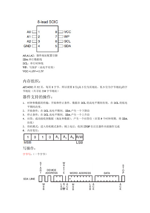
A0,A1,A2:器件地址配置引脚
SDA:串行数据线
SCL:串行时钟线
WP:写保护(高电平有效)
VCC:+1.8V~+5.5V
内存组织:
AT24C02:共32页,每页8字节。
所以需要8位(高5位为页地址,低3位为字节地址)的字节地址(共寻址256字节地址)
器件支持的操作:
1、时钟和数据的传输:开始和停止条件,数据在SCL的高电平期间有效,在SCL的低电
平期间改变。
2、开始条件:在SCL高电平期间,SDA产生一个下降沿
3、停止条件:在SCL高电平期间,SDA产生一个上升沿
4、应答:成功接收到数据(地址和数据),产生一个应答位(在第9个时钟周期,将SDA
拉低)
5、待机模式:进入待机模式条件:刚上电后;收到STOP位后且器件内部操作完成
6、内存复位:
写操作:
字节写:(一个字节)
页写:(最多8个字节)
当写到一页的末尾后,如果再写入数据,则从同一页的开始处写入,而覆盖原来的数据。
应答查询:一旦器件内部定时编程数据开始,则EEPROM对输入是不反映的。
发送一个开始信号和器件地址,要是EEPROM内部编写完成,将应答(将SDA拉低),以使下一个读或写操作继续。
读操作:
当前地址读:(一个字节)
内部数据地址计数器保存着最后一次的操作地址(读或写)。
只要芯片一直上电,该地址一直有效。
当读到内存的最后字节后,指针将回到第一页的开始地址,而对于写操作,从当前也的最后返回到同一页的第一个字节处。
任意读:(一个字节)
连续读:(是从当前地址读或任意读开始的)。

24c02中文资料1. 简介24c02是Microchip公司推出的一种串行电子可擦写可编程读写存储器,属于EEPROM(Electrically Erasable Programmable Read-Only Memory)系列。
它采用2-wire串行总线(I2C)接口,具有体积小、功耗低、可靠性高等特点。
本文档将详细介绍24c02的硬件特性、接口规范、存储容量和使用方法。
2. 硬件特性24c02的主要硬件特性如下:•存储容量:24c02有256个字节,每个字节有8位,总计拥有2Kb的存储空间。
•工作电源:24c02需要使用3.3V到5V的供电电压,支持广泛的电源电压范围。
•通信接口:24c02使用I2C串行总线进行通信,具有两根信号线:串行数据线(SDA)和串行时钟线(SCL)。
•封装类型:24c02有多种封装类型可供选择,如DIP(双列直插式封装)、SOP(小型轻负载封装)等。
3. 接口规范24c02采用I2C串行总线接口,其接口规范如下:•数据传输方式:24c02支持字节读写操作和页写操作。
字节读写操作是指每次读写一个字节的数据;页写操作是指每次可以写入8个连续字节的数据。
•起始信号和停止信号:在I2C总线上进行通信时,需要发送起始信号(Start)和停止信号(Stop)以标识数据传输的开始和结束。
•从器件地址:24c02有多个从器件地址可供选择,通过设置硬件地址引脚,可以实现多个24c02器件的级联。
4. 存储容量24c02的存储容量为2Kb,相当于256个字节。
每个字节有8位,可存储0x00到0xFF的数据。
这些存储空间可以被分为多个页,每页包含8个字节。
5. 使用方法以下是24c02的基本使用方法,供参考:•初始化:将24c02与主控芯片(如单片机)连接,并提供正常的供电电源。
同时,设置24c02的硬件地址引脚,确保能正确寻址。
•写入数据:选择要写入数据的存储地址,发送起始信号和器件地址,然后发送数据字节。
EEPROM存储芯⽚24C021、24C02简介 24C02是⼀个2Kbit的串⾏EEPROM存储芯⽚,可存储256个字节数据。
⼯作电压范围为1.8V到6.0V,具有低功耗CMOS技术,⾃定时擦写周期,1000000次编程/擦除周期,可保存数据100年。
24C02有⼀个16字节的页写缓冲器和⼀个写保护功能。
通过I2C总线通讯读写芯⽚数据,通讯时钟频率可达400KHz。
可以通过存储IC的型号来计算芯⽚的存储容量是多⼤,⽐如24C02后⾯的02表⽰的是可存储2Kbit的数据,转换为字节的存储量为2*1024/8 = 256byte;有⽐如24C04后⾯的04表⽰的是可存储4Kbit的数据,转换为字节的储存量为2*1024/8 = 512byte;以此来类推其它型号的存储空间。
24C02的管脚图如下: VCC和VSS是芯⽚的电源和地,电压的⼯作范围为:+1.8V~+6.0V。
A0、A1、A2是IC的地址选择脚。
WP是写保护使能脚。
SCL是I2C通讯时钟引脚。
SDA是I2C通讯数据引脚。
2、24C02的设备地址和写保护功能 I2C主机在与24C02通讯时,需要发送⼀个设备地址进⾏寻址,在I2C总线上,每⼀个从机设备的地址都是唯⼀的。
24C02的设备地址包含两部分,第⼀部分是bit7~bit4是固定的“1010”,第⼆部分bit3~bit1位由A2、A1、A0组成。
主机在与24C02进⾏通讯时,除了发送设备地址还需要发送数据的读写⽅向位R/W,24C02的是设备地址与R/W位组成了⼀个字节的数据。
如下图: 上图列出了⼏个存储IC的设备地址与R/W位组成的字节。
由图中可以看到,存储IC地址的bit7~bit4位固定为“1010”;bit3~bit1位由A2、A1、A0引脚的电平状态决定,如果Ax接的是电源(⾼电平),那么Ax=1,如果Ax接的是地,那么Ax=0,即由A2、A1、A0可以组合成8种设备地址,也就是说在同⼀个I2C总线上可以同时挂载8个24C02芯⽚。
24C02/24C04/24C08/24C16/24C32/24C641.2.2K4K 8K ,16K ,32K 位和64K 位串行I C 总线EEPROM3.24C02/04/08/16/32/64PROM256/512/1024/2048/4096/8192×8-bit1.8V1μA1mA 24C02/04/08/16/32/648/16/16/16/32/3224C02/04/08/16/32/648-pin PDIP8-pin SOP ●●●●●●●●●●●●SD SCL WP V CC NC A SD A SCL WP V CC 12348765NC NC NC GND SD A SCL WP V CC 12348765 ()SD A SCL WP V CC 12348765A 0A 1A 2GND C02C1621.8V~5.5V- 1mA- 1μA- 24C02, 256 X 8 (2K bits)- 24C04, 512 X 8 (4K bits) - 24C08, 1024 X 8 (8K bits) - 24C16, 2048 X 8 (16K bits)- 24C32, 4096 X 8 (32K bits)- 24C64, 8192 X 8 (64K bits)2I CI C 1 MHz (5V), 400 kHz (1.8V, 2.5V, 2.7V) ( 5 ms)8 (24C02)16(24C04/08/16),32字节页(24C32/64)ESD 2.5kV - 100- 100 8-pin DIP 8-pin SOP RoHS ●●●●●●●22●S D A 123487651A 2GND NC NC C A 2GND C04C082.7V)00n SOP●●SD A SCL WP V CC 12348765A 0A 1A 2GND C32SD ASCL WP V CC 12348765A 0A 1A 2GNDC6424C02/24C04/24C08/24C16/24C32/24C645. Ḛ1 ḚV 6. 乱 ヺ ԡⳈ⌕կ⬉⬉ Ⳉ⌕䕧 ⬉ ⏽V CC Ⳉ⌕䕧 ⬉ V IN V OUT T STG -0.3 ~ V CC +0.3-0.3 ~ V CC +0.3-0.3 ~ +6.5°C -65 ~ +150V °C7. 㤤 ӊヺ ԡⳈ⌕կ⬉⬉ V CC ⏽T A+855.5 1.8-40(䍙 乱 㛑Ӯ 㟈 ӊ )V V ( 㤤 ӊϟ ⦄ 㛑)SDASCL WP V CCNC /NC /NC /A0NC /NC /A1/A1NC /A2/A2/A2C16/C08/C04/C02GNDSTART STOPLOGICSERIAL CONTROLLOGICDEVICE ADDRESS COMPARATORDATA WORD ADDRESS COUNTER LOADCOMPLOADINCY DECODER HIGH VOLTAGE PUMP/TIMING ENDATA RECOVERYEEPROMSERIAL MUXX D E C O D E RDOUT/ACKNOWLEDGEDINESD ⬉ (Ҏԧ )ESD ⬉ ( )V ESD2500200V V乱⬉ 䕧 ⬉ 乱 㛑Ӯ 㟈 ӊ DOUTmA 9. Ⳉ⌕⬉⇨⡍ヺ ԡ ⬉⌕կ⬉⬉⌕I CC V CC =5V⌟䆩 ӊ100kHz 3.0䕧 Ԣ⬉ ⬉μA 3.01.0-0.6V 0.4V IN = V CC GND 0.05( ӊ˖T A = 0°C ̚ +70°C, V CC = +1.8V ̚ +5.5V ˈ䰸䴲 ⊼䞞)䕧 Ԣ⬉ ⬉ μA V IL 0.4V CC0.20.4100kHz V V CC ×0.3I SB V IN = V CC GND V OUT = V CC GND μA 䕧 ⓣ⬉⌕䕧 ⓣ⬉⌕I LI I LO V IH 䕧 催⬉ ⬉ V CC +0.5V V V VV OL3V OL2V = 2.1 mA V 10. Ѹ⌕⬉⇨⡍ ( ӊ˖T A = 0°C ̚ +70°C, V = +1.8V +5.5V, C L = 100 pF ˈ䰸䴲 ⊼䞞)ヺ ԡ䩳催⬉䩳乥⥛, SCL ⌟䆩 ӊ400V CC =1.8V 1000ns 0.050.050.60.90.6 μskHz 1.20.5540V CC =5V 0.4t LOW μs ⍜䰸 䯈 䩳ϟ䰡⊓ 䕧 䯈䱨 䯈t I t AA50t HIGH䩳Ԣ⬉ μsV CC =1.8V V CC =5V V CC =1.8V V CC =5V V CC =1.8V V CC =5V V CC =1.8V V CC =5V8. 㛮⬉( ӊ˖T A = 25°C, f = 1.0 MHz, V CC = +1.8V)pFヺ ԡ䕧 /䕧 ⬉ (SDA)C I/O 䕧 ⬉ (A0, A1, A2, SCL)C IN68 pF⌟䆩 ӊV I/O = 0V V IN = 0V1.2 㒓䞞 䯈t BUF0.5μs V CC =1.8V V CC =5V䇏1.03.0 mA m 042.0C =5.0V, I OL = 3.0 mA CC ×0.7GNDOL1V CC =3.0V, I OL =2.1mA CC =1.8V, I OL = 0.15 mA =C CC = +1.8V ̚+5.5f SCL10. Ѹ⌕⬉⇨⡍ (㓁)䕧 Ϟ 䯈 䕧 䯈0ns500.650.25ns t WRns 100ns ℶ ӊ ゟ 䯈 䕧 䯈t R t DH t F 䕧 ゟ 䯈μs ms䕧 ϟ䰡 䯈t SU.STOV CC =1.8V V CC =5V V CC =1.8V V CC =5Vμs 300100300t HD.DAT t SU.DAT 2 㒓3SCLSDA_INSDA _OUTt F t LOWt SU .STAt HD.STAt AA t DHt BUFt SU.STOt Rt HD.DAT t SU.DAT t HIGH t LOW8th BIT SCLSDAACKSTOPCONDITIONSTART CONDITIONt WR (1)t HD.STAμs 䍋 ӊ 䯈䍋 ӊ ゟ 䯈t SU.STA V CC =1.8V V CC =5V V CC =1.8V V CC =5Vμs 0.60.250.60.25ヺ ԡ ⌟䆩 ӊ ⊼ 䯈W :5 ҢϔϾ ⱘ ℶ ӊ 㟇 䚼 㒧 ⱘ 䯈DŽn 08V μ3001AHIG11.3156247A0A1A2SDA SCL WP GND V CCA2A1A024C02/32/64A2A1A0824C02/32/6424C04A2A1424C04A024C08A2224C08A0A124C1616KA2A1A0/SDA V CC10kΩSCL8WP WPWPV CC12.13. 䆺㒚 䇈24CXX I C 㒓Ӵ䕧 䆂DŽI C ϔ⾡ ǃϸ㒓І㸠䗮䆃 ˈ І㸠 㒓SDA І㸠 䩳㒓SCL DŽϸḍ㒓䛑 乏䗮䖛ϔϾϞ ⬉䰏 ⬉⑤DŽ ⱘ 㒓䜡㕂 4 ⼎4 ϸ㒓 㒓䜡㕂㒓Ϟ 䗕 ⱘ ӊ㹿⿄ 䗕 ˈ ⱘ ӊ㹿⿄ DŽ Ѹ ⱘ ӊ㹿⿄Џ ӊˈ Џ ӊ ⱘ ӊ 㹿⿄Ң ӊDŽЏ ӊѻ⫳І㸠 䩳SCL ˈ㒓ⱘ䆓䯂⢊ ǃѻ⫳START STOP ӊDŽ24CXX I C 㒓ЁЎҢ ӊ DŽ㒓 Ѣぎ䯆⢊ ҹ Ӵ䕧DŽ↣ Ӵ䕧 ѢSTART ӊˈ㒧 ѢSTOP ӊˈѠ㗙П䯈ⱘ 㡖 ≵ 䰤 ⱘˈ⬅ 㒓ϞⱘЏ ӊ DŽ ҹ 㡖˄8ԡ˅Ў ԡӴ䕧ˈ9ԡ ⬅ ѻ⫳ ㄨDŽ䍋 ℶ ӊ䩳㒓䛑Ў催 ⿄ 㒓 ぎ䯆⢊ DŽ SCL Ў催⬉ SDA ⱘϟ䰡⊓˄催 Ԣ 䍋 ӊ˄START ˈㅔ ЎS ˅ˈSDA ⱘϞ ⊓˄Ԣ 催˅ ℶ ӊ˄STOP ˈㅔ ЎP ˅DŽ 㾕 5DŽ5 䍋 ӊ ℶ ӊⱘ НV CCҪ24Cxx MPU SDASCLR PR Pϸ㒓І㸠S Ў催ㅔ ЎⱘϞ ⊓˄Ԣ 㒓І㸠 㒓SS 䍋 ӊ222ԡӴ䕧↣Ͼ 䩳㛝 Ӵ䗕ϔԡ DŽSCL Ў催 SDA 乏 〇 ˈ Ўℸ SDA ⱘ 㹿䅸Ў DŽԡӴ䕧 㾕 6DŽ6 ԡӴ䕧ㄨ㒓Ϟⱘ ↣ ϔϾ 㡖 ѻ⫳ϔϾ ㄨˈЏ ӊ 乏ѻ⫳ϔϾ ⱘ乱 ⱘ 䩳㛝 ˈ㾕 7DŽ7 I C㒓ⱘ ㄨ ԢSDA 㒓㸼⼎ ㄨˈ ㄨ㛝 䯈 〇 ⱘԢ⬉ DŽ Џ ӊ ˈ 乏 Ӵ䕧㒧 ⱘ 㒭 䗕 ˈ ϔϾ 㡖П ⱘ ㄨ㛝 䯈ϡӮѻ⫳ ㄨ ˄ϡ ԢSDA ˅DŽ䖭⾡ ϟˈ 䗕 乏䞞 SDA 㒓Ў催ҹ Џ ӊѻ⫳ ℶ ӊDŽ䗕 䕧 ⱘ䕧 ⱘЏ ӊ ⱘ䍋 ӊ289䴲 ㄨㄨㄨ 䩳㛝㒓〇䆌SDASCL2ѻ⫳ϔϾ ㄨˈЏ ӊ 乏ѻ⫳ϔԢ㒓Ӵӊ ⱘSCL 䍋 ӊS1ӊ䍋 ӊՓ㛑㢃⠛䇏 ˈEEPROM 䛑㽕∖ 8ԡⱘ ӊ ˄㾕 8˅DŽӊ ⬅"1"ǃ"0" 㒘 ˈ 4ԡ Ё ⼎ˈ Ѣ І㸠EEPROM 䛑 ϔḋⱘ Ѣ24C02/32/64ˈ䱣 3ԡA2ǃA1 A0Ў ӊ ԡˈ 乏Ϣ⹀ӊ䕧 㛮 ϔ㟈DŽ Ѣ24C04ˈ䱣 2ԡA2 A1Ў ӊ ԡˈ 1ԡЎ义 ԡDŽA2 A1 乏Ϣ⹀ӊ䕧 㛮 ϔ㟈ˈ㗠A0 ぎ㛮DŽѢ24C08ˈ䱣 1ԡA2Ў ӊ ԡˈ 2ԡЎ义 ԡDŽA2 乏Ϣ⹀ӊ䕧 㛮 ϔ㟈ˈ㗠A1 A0 ぎ㛮DŽѢ24C16ˈ ӊ ԡˈ3ԡ䛑Ў义 ԡˈ㗠A2ǃA1 A0 ぎ㛮DŽ ӊ ⱘLSB Ў䇏/ 䗝 ԡˈ催Ў䇏 ˈԢЎ DŽ㢹↨䕗 ӊ ϔ㟈ˈEEPROM 䕧 ㄨ"0"DŽ ϡϔ㟈ˈ 䖨 ⢊ DŽ8 ӊ 1010A2A1A0R/W MSBLSB1010A2A1P0R/W1010A2P1P0R/W1010P2P1P0R/Wӊ EEPROM Ԣ 㗫 ⱘ⡍⚍ˈ ӊЎ˖˄1˅⬉⑤Ϟ⬉˗˄2˅ ℶ ӊ ӏԩ 䚼 DŽ24C0424C0824C16DŽ ԡ䆂Ёѻ⫳Ё ǃ ⬉ ㋏㒳 ԡ ˈI C 㒓 䗮䖛ҹϟℹ偸 ԡ˖ ˄1˅ѻ⫳9Ͼ 䩳 DŽ˄2˅ SCL Ў催 ˈSDA гЎ催DŽ ˄3˅ѻ⫳ϔϾ䍋 ӊDŽ21. 㡖㽕∖ ӊ ACK ㄨ ˈ 8ԡⱘ DŽ 䖭Ͼ EEPROM ㄨ"0"ˈ✊ ϔϾ8ԡ DŽ 8ԡ ˈEEPROM ㄨ"0"ˈ ⴔ 乏⬅Џ ӊ 䗕 ℶ ӊ 㒜ℶ DŽℸ EEPROM 䖯 䚼 t WR ˈ 䴲 Ёˈ ℸ 䯈 䕧 䛑 Ⳉ ˈEEPROM Ӯ ㄨ˄㾕 9˅DŽ9 㡖SDA 㒓䍋 ӊM S BL S B R /W A C K M S BL S B A C KA C Kӊℶ ӊDŽ24C02/32/6413.2.图10页写24C02器件按8字节/页执行页写,24C04/08/16器件按16字节/页执行页写,24C32/64器件按32字节/页执行页写。
CA T24C 161/162(16K),CAT24C081 /082(8K) CAT24C041/042(4K),CAT24C021/022(2K)I2C串行CMOS E2PROM,精确的复位控制器和看门狗定时器控制电路特性•数据线上的看门狗定时器(仅对CA T24Cxxl)籲可编程复位门槛电平籲高数据传送速率为400KHz和I2C总线兼容• 2.7V至6V的工作电压•低功耗CMOS工艺籲16字节页写缓冲区籲片内防误擦除写保护籲高低电平复位信号输出——精确的电源电压监视器——可选择5V、3.3V和3V的复位门槛电平•100万次擦写周期•数据保存可长达100年•8脚DIP或SOIC封装•商业级、工业级和汽车温度范围概述CA T24Cxxx是集E2PROM存储器,复位微控制器和看门狗定时器三种流行功能与一体的芯片。
CAT24C161/162 (16K),CAT24C081/082 (8K),CA T24C041/042 (4K)和CAT24C021/022 (2K)以I2C是串行CMOS E2PROM器件。
釆用CMOS工艺大降低了器件的功耗。
CA T24Cxxx 另一特点是16字节的页写缓冲区,提供8脚DIP和SOIC 封装。
CA T24Cxxx的复位功能和看门狗定时器功能保证系统出现故障的时候能给CPU —个复位信号。
CA T24Cxxx 的2脚输出低电平复位信号,7脚输出高电平复位信号。
CAT24Cxxl看狗溢出信号从SDA脚输出。
CAT24Cxx2不具备看门狗功能。
绝对最大参数工作温度:-55°C〜125°C贮存温度:-65°C〜15°C各管脚承受对地电压:-2.0V〜Vcc+2.0V VCC对地电压范围:-2.0V〜7.0V 最大功耗: 1.0W管脚焊接温度(10S): 300 °C输出短路电流:100mA管脚配置]V C C ]RESET方框图表一直流操作特性表二上电时序管脚介绍WP:写保护将该管脚接Vcc,E2PRON就实现写保护(只读)。