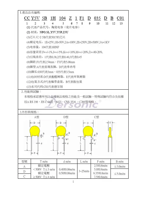
高压电容器PDF
- 格式:pdf
- 大小:428.62 KB
- 文档页数:18
October 2009Doc ID 9343 Rev 51/8STTH112High voltage ultrafast rectifierFeatures■Low forwarded voltage drop ■High reliability■High surge current capability■Soft switching for reduced EMI disturbances ■Planar technologyDescriptionThe STTH112, which is using ST ultrafast high voltage planar technology, is specially suited for free-wheeling, clamping, snubbering,demagnetization in power supplies and other power switching applicationsTable 1.Device summarySymbol Value I F(AV) 1 A V RRM 1200 V T j (max) 175 °C V F (max)1.65 VElectrical characteristics STTH1122/8Doc ID 9343 Rev 51 Electrical characteristicsAbsolute ratings (limiting values)Symbol ParameterValue Unit V RRM Repetitive peak reverse voltage 1200V V (RMS)Voltage rms850VI F(AV)Average forward currentTl = 85°C δ =0.5DO-411ATl = 115°C δ =0.5SMA Tl = 125°C δ =0.5SMBI FSMForward surge current t = 8.3 ms DO-4120ASMA 18SMBT stg Storage temperature range- 50 + 175°C T jMaximum operating junction temperature+ 175°CTable 2.Thermal parametersSymbolParameterValue UnitR th (j-l)Junction to leadL = 10 mmDO-4145°C/W SMA 30SMB25R th (j-a)Junction to ambient L = 10 mm DO-41110Table 3.Static electrical characteristicsSymbol ParameterTests conditions Min.Typ.Max.Unit I RReverse leakage currentV R = 1200 VT j = 25 °C 5µAT j = 125 °C 50V FForward voltage dropI F = 1 A T j = 25 °C1.9V T j = 125 °C 1.17 1.65T j = 150 °C1.101.55Table 4.Dynamic electrical characteristicsSymbol ParameterTests conditionsMin.Typ.Max.Unit t rr Reverse recovery time I F = 0.5 AI rr = 0.25 A I R = 1A T j = 25 °C 75ns t fr Forward recovery time I F = 1 AdI F /dt = 50 A/µs V FR = 1.1 x V FmaxT j = 25 °C500ns V FPForward recovery voltage30VSTTH112Electrical characteristicsDoc ID 9343 Rev 53/8Figure 1.Conduction losses versus averageFigure 2.Forward voltage drop versusFigure 3.Relative variation of thermal impedance junction ambient versus Figure 4.Relative variation of thermalimpedance junction ambient versusFigure 5.Relative variation of thermal impedance junction ambient versus Figure 6.Thermal resistance junction to ambient versus copper surfaceElectrical characteristics STTH112 Figure 7.Thermal resistance junction to ambient versus copper surface under each lead4/8Doc ID 9343 Rev 5STTH112Package informationDoc ID 9343 Rev 55/82 Package information●Epoxy meets UL 94, V0●Band indicates cathode●Bending method (DO-41): see Application note AN1471In order to meet environmental requirements, ST offers these devices in different grades ofECOPACK ® packages, depending on their level of environmental compliance. ECOPACK ® specifications, grade definitions and product status are available at: . ECOPACK ® is an ST trademark.Table 5.SMA dimensionsRef.DimensionsMillimeters Inches Min.Max.Min.Max.A1 1.90 2.450.0750.094A20.050.200.0020.008b1.25 1.650.0490.065c0.150.400.0060.016D 2.25 2.900.0890.114E4.805.350.1890.211E1 3.95 4.600.1560.181L0.751.500.0300.059ECLE1DA1A2bPackage informationSTTH1126/8Doc ID 9343 Rev 5Table 7.DO-41 (plastic) dimensionsRef.DimensionsMillimeters Inches Min.Max.Min.Max.A4.075.200.1600.205B 2.04 2.710.0800.107C 25.41D0.710.860.0280.034ØD ØBACCSTTH112Ordering informationDoc ID 9343 Rev 57/83 Ordering information4 Revision historyTable 8.Ordering informationOrder code Marking Package Weight Base qty Delivery Mode STTH112STTH112DO-41 0.34 g 2000Ammopack STTH112A H12SMA 0.068 g 5000Tape and reel STTH112U U12SMB 0.11 g 2500Tape and reel STTH112RLSTTH112DO-410.34 g5000Tape and reelTable 9.Document revision historyDate RevisionChangesJan-20032Initial release.22-Jun-20053New value of T j = 150 °C added to table 2.Dimensions A1 E and D updated in T able 4. Data sheet reformatted. No other technical changes.20-Mar-20074Reformatted to current standards. Updated dimensions and footprints for SMA and SMB packages.30-Sep-20095Updated table 7 package dimensions.STTH112Please Read Carefully:Information in this document is provided solely in connection with ST products. STMicroelectronics NV and its subsidiaries (“ST”) reserve the right to make changes, corrections, modifications or improvements, to this document, and the products and services described herein at any time, without notice.All ST products are sold pursuant to ST’s terms and conditions of sale.Purchasers are solely responsible for the choice, selection and use of the ST products and services described herein, and ST assumes no liability whatsoever relating to the choice, selection or use of the ST products and services described herein.No license, express or implied, by estoppel or otherwise, to any intellectual property rights is granted under this document. If any part of this document refers to any third party products or services it shall not be deemed a license grant by ST for the use of such third party products or services, or any intellectual property contained therein or considered as a warranty covering the use in any manner whatsoever of such third party products or services or any intellectual property contained therein.UNLESS OTHERWISE SET FORTH IN ST’S TERMS AND CONDITIONS OF SALE ST DISCLAIMS ANY EXPRESS OR IMPLIED WARRANTY WITH RESPECT TO THE USE AND/OR SALE OF ST PRODUCTS INCLUDING WITHOUT LIMITATION IMPLIED WARRANTIES OF MERCHANTABILITY, FITNESS FOR A PARTICULAR PURPOSE (AND THEIR EQUIVALENTS UNDER THE LAWS OF ANY JURISDICTION), OR INFRINGEMENT OF ANY PATENT, COPYRIGHT OR OTHER INTELLECTUAL PROPERTY RIGHT. UNLESS EXPRESSLY APPROVED IN WRITING BY AN AUTHORIZED ST REPRESENTATIVE, ST PRODUCTS ARE NOT RECOMMENDED, AUTHORIZED OR WARRANTED FOR USE IN MILITARY, AIR CRAFT, SPACE, LIFE SAVING, OR LIFE SUSTAINING APPLICATIONS, NOR IN PRODUCTS OR SYSTEMS WHERE FAILURE OR MALFUNCTION MAY RESULT IN PERSONAL INJURY, DEATH, OR SEVERE PROPERTY OR ENVIRONMENTAL DAMAGE. ST PRODUCTS WHICH ARE NOT SPECIFIED AS "AUTOMOTIVE GRADE" MAY ONLY BE USED IN AUTOMOTIVE APPLICATIONS AT USER’S OWN RISK.Resale of ST products with provisions different from the statements and/or technical features set forth in this document shall immediately void any warranty granted by ST for the ST product or service described herein and shall not create or extend in any manner whatsoever, any liability of ST.ST and the ST logo are trademarks or registered trademarks of ST in various countries.Information in this document supersedes and replaces all information previously supplied.The ST logo is a registered trademark of STMicroelectronics. All other names are the property of their respective owners.© 2009 STMicroelectronics - All rights reservedSTMicroelectronics group of companiesAustralia - Belgium - Brazil - Canada - China - Czech Republic - Finland - France - Germany - Hong Kong - India - Israel - Italy - Japan - Malaysia - Malta - Morocco - Philippines - Singapore - Spain - Sweden - Switzerland - United Kingdom - United States of America8/8Doc ID 9343 Rev 5Mouser ElectronicsAuthorized DistributorClick to View Pricing, Inventory, Delivery & Lifecycle Information:S TMicroelectronics:STTH112RL STTH112U STTH112A。
耐压等级最高的片式钽电容器片式钽电容器的阴极采用电子电导型的二氧化锰作为产品阴极,二氧化锰生产的电解电容器具有非常强的自我修补能力,因此,自60年代问世以来,目前为止,它仍然是中高压固体钽电容器最合适的阴极材料。
尽管近些年已经出现了高频阻抗更低的3,4乙烯二氧噻吩[聚噻吩]作阴极的高分子片式钽电容器,但由于高分子阴极的电阻率太低,因此,它不能使用在16V以上的钽电容器上。
在生产二氧化锰作阴极的片式钽电容器时,二氧化锰阴极使用化学分解的方法来制造,由于产品反复经过多次的高温化学分解,因此,在生产结束时,产品的耐压将有大幅度下降。
为了弥补化学分解制造阴极时导致的耐压下降问题,一般在决定产品耐压高低的介质层形成时,必须使用远远高于额定电压的形成电压来形成介质层。
一般使用的介质层形成电压和额定电压的比例为4:1。
也就是说额定电压为50V的产品的介质层形成电压必须达到200V 以上产品的耐压才可以保证。
而由于体积限制,片式钽不同壳号的尺寸采用IEC标准,因此装粉量受到严格限制。
同时,受制于生产钽电容器使用的钽粉生产技术水平的限制,在有限的壳号内,片式钽电容器的最高耐压一般最高只能达到50V的水平。
片式钽最大的使用电路基本上都是高浪涌高纹波的开关电源电路,使用在此类低阻抗电路,使用电压只能达到额定电压的1/3,为存在的浪涌留出足够的余量才可以保证安全和可靠性能够达到整机的可靠性要求。
因此,50V的片式钽在此类电路的上限使用电压不能超过16V,如果电路中的供电电流较小[例如使用电池供电的电路],使用电压才可以达到额定电压的1/2。
当此类电路的使用电压较高时,特别是高可靠的军用电路,必须使用耐压更高的片式钽电容器才可以达到高可靠要求。
为了达到特殊的军用电路要求,北京718电子有限责任公司专门开发了一种新型的片式钽电容器,此产品使用了最新的高可靠材料和最新的介质层形成技术,产品的耐压可以达到63V以上。
产品的温度特性极为优良,在-55-+125度内,容量变化率在-3-+3%以内。
高比能高压脉冲电容器高比能高压脉冲电容器,需要从如下2个方面来理解:①高压脉冲电容器②高比能。
高压脉冲电容器是一种储能器,它能够在一个较长的时间间隔内由一个功率不大的电源充电,把能量储存在电容器中,在需要的时候,能够在极短的时间间隔内放出强大的冲击电流和脉冲功率。
强大的冲击电流和脉冲功率可以产生出极高的温度,强大的电磁场和冲击波。
在高压试验、激光技术,核子研究、地质勘探、等离子技术和火箭技术等方面都有着相当广泛的应用。
[1]高比能,指的是在有限的体积下能提供非常高的能量,或者叫做高储能密度。
适用于对体积有一定限制的条件下,要求能提供足够大的能量的电容器的应用。
广泛应用于脉冲电源、医疗器械、电磁武器、粒子加速器以及环保领域。
[2]中文名高比能高压脉冲电容器外文名High energy density high voltage pulse capacitor从电容器能量公式W=½UQ=½CU²[3]可知:需要获得高的能量,需要提高电容量(C)或者电压(U)。
所以一般高比能脉冲电容器需要用金属化薄膜或者箔式结构来制作,因为金属化薄膜和箔式结构的电容器能把电容量(U)做到uF和mF以上,而陶瓷电容的电容量基本都是pF级别。
1F=1000,000微法=10微法(uF)1uF=1000,000皮法=10皮法(PF)[4]高比能也称高储能密度,储能比=能量/体积。
也就是说单位体积内,储存的能量越多比能越大。
高储能密度脉冲电容器的储能密度由几十J/L升至KJ/L,国内部分厂家在试验室已能做到2~3KJ/L,能实现量产的有CABO脉冲电容器。
能够量产2~3kJ/L的厂商主要集中在美国,有Aerovox,Maxwell lab.,Sangomo 等。
Maxwell lab.、Averovox和ABB公司在高储能密度金属化膜电容器的研究、开发和生产上处于领先水平,可惜国外对改类产品实行技术封锁,国内几乎买不到。