450nm50mw欧司朗蓝色激光器技术规格书
- 格式:pdf
- 大小:1.60 MB
- 文档页数:2
LED020侧发光蓝光规格书产品型号:YT-020B 蓝光适用于: 顺向电流 IF=20mA目录1.特性2.应用范围3.产品外观尺寸4.最大绝对标称值5.光电特性参数6.典型光电参数曲线7.编带规格8.包装方式9.BIN级范围10.可靠度实验项目及条件11.使用注意事项1、特性:1.1 封装尺寸:3.8x1.0x0.6mm1.2发光颜色:蓝色1.3胶体颜色:无色透明1.4焊接方式:回流焊1.5符合RoHS 标准2、应用范围:2.1手机按键2.2一般应用3、成品外观尺寸:备注:1.所有尺寸均以mm 为单位4、最大绝对标称值(环境温度=25℃):5.光电特性参数(环境温度=25℃):备注:1.亮度偏差:±5% 2.电压偏差:±0.033.主波长偏差:±16.典型光电参数曲线40IF(mA)IF(mA)80 604020Vf(V)0.020.0 40.0 60.0 80.0 Ta(°C)100.0 FIG.1 FORWARD CURRENT VS. FORWARD VOLTAGE.FIG.2 MAXIMUM FORWARD DC CURRENT VSAMBIENT TEMPERATURE(Tjmax=105 °C)Half PowerWL=150nmI (RELATIVE LUMINOUS INTENSITY)5.04.03.02.01.00.0 0.020.040.060.080.0If(mA) 100.0400600 FIG.3 RELATIVE LUMINOUS INTENSITY VS. FORWARD CURRENTFIG.4 RELATIVE LUMINOUS INTENSITY VS. WAVELENGTH.50% Power Angle:120°0°le(%)100%80%60%40%20%-90°-60°-30° 0 30° 60°0%90°FIG.5 FAR FIELD PATTERN7. 编带规格:(单位:mm )包装数量 1000-4000pcs/卷8.包装方式:(单位:mm)9.BIN 级范围正向电压VF(公差:±0.05V):20MA测试亮度IV(公差:±5%):10.可靠度实验项目及条件:可靠度实验不合格判定标准:IV:衰减超过 30%VF:变化超过 20%备注:1、同一项实验结果的测试需在 2 个小时之内完成;2、测试必须在每项实验完成后、材料恢复正常环境条件下才能进行.11.使用注意事项11.1焊接SMD LED 灌封胶较软,外力易损坏发光面及塑料壳,焊接时要轻拿轻放。
Part NumberEmitting Color (Material)Lens TypeIv (mcd) @ 20mA [2] Viewing Angle [1]Min. Typ. 2θ1/2L-7104PBC-A■ Blue (InGaN)Water Clear 400 30°900DESCRIPTIONSzThe Blue source color devices are made with InGaN on SiC Light Emitting Diodez Electrostatic discharge and power surge could damage the LEDsz It is recommended to use a wrist band oranti-electrostatic glove when handling the LEDs z All devices, equipments and machineries must be electrically groundedFEATURESzLow power consumptionz Popular T-1 diameter package z General purpose leads z Reliable and ruggedz Long life - solid state reliability z Available on tape and reel z RoHS compliantAPPLICATIONSz Status indicator z Illuminatorz Signage applicationsz Decorative and entertainment lightingzCommercial and residential architectural lightingATTENTIONObserve precautions for handlingelectrostatic discharge sensitive devicesPACKAGE DIMENSIONSL-7104PBC-AT-1 (3mm) Solid State LampSELECTION GUIDENotes:1. θ1/2 is the angle from optical centerline where the luminous intensity is 1/2 of the optical peak value.2. Luminous intensity / luminous flux: +/-15%.3. Luminous intensity value is traceable to CIE127-2007 standards.Notes:1. All dimensions are in millimeters (inches).2. Tolerance is ±0.25(0.01") unless otherwise noted.3. Lead spacing is measured where the leads emerge from the package.4. The specifications, characteristics and technical data described in the datasheet are subject to change without prior notice.ABSOLUTE MAXIMUM RATINGS at T A =25°CELECTRICAL / OPTICAL CHARACTERISTICS at T A =25°CNotes:1. 1/10 Duty Cycle, 0.1ms Pulse Width.2. 2mm below package base.3. 5mm below package base.4. Relative humidity levels maintained between 40% and 60% in production area are recommended to avoid the build-up of static electricity – Ref JEDEC/JESD625-A and JEDEC/J-STD-033.Notes:1. The dominant wavelength (λd) above is the setup value of the sorting machine. (Tolerance λd : ±1nm. )2. Forward voltage: ±0.1V.3. Wavelength value is traceable to CIE127-2007 standards.4. Excess driving current and / or operating temperature higher than recommended conditions may result in severe light degradation or premature failure.ParameterSymbol Value Unit Power Dissipation P D 120 mW Reverse Voltage V R 5 V Junction Temperature T j 125 °C Operating Temperature T op -40 to +85 °C Storage Temperature T stg -40 to +85°C DC Forward Current I F 30 mA Peak Forward CurrentI FM [1]100 mA Electrostatic Discharge Threshold (HBM) -1000VLead Solder Temperature [2] 260°C For 3 Seconds Lead Solder Temperature [3]260°C For 5 SecondsParameterSymbol Emitting ColorValue Unit Typ. Max. Wavelength at Peak Emission I F = 20mA λpeak Blue 468 - nm Dominant Wavelength I F = 20mA λdom [1] Blue 465 - nm Spectral Bandwidth at 50% Φ REL MAX I F = 20mA Δλ Blue 21 - nm CapacitanceC Blue 100 - pF Forward Voltage I F = 20mA V F [2] Blue 3.2 4 V Reverse Current (V R = 5V)I RBlue-10uATECHNICAL DATABLUERECOMMENDED WAVE SOLDERING PROFILENotes:1. Recommend pre-heat temperature of 105°C or less (as measured with a thermocoupleattached to the LED pins) prior to immersion in the solder wave with a maximum solder bath temperature of 260°C2. Peak wave soldering temperature between 245°C ~ 255°C for 3 sec (5 sec max).3. Do not apply stress to the epoxy resin while the temperature is above 85°C.4. Fixtures should not incur stress on the component when mounting and during soldering process.5. SAC 305 solder alloy is recommended.6. No more than one wave soldering pass.PACKING & LABEL SPECIFICATIONSPRECAUTIONSStorage conditions1. Avoid continued exposure to the condensing moisture environment and keep the product away from rapid transitions in ambient temperature.2. LEDs should be stored with temperature ≤ 30°C and relative humidity < 60%.3. Product in the original sealed package is recommended to be assembled within 72 hours of opening. Product in opened package for more than a week should be baked for 30 (+10/-0) hours at 85 ~ 100°C.2. When soldering wires to the LED, each wire joint should be separately insulated with heat-shrink tube to prevent short-circuit contact. Do not bundle both wires in one heat shrink tube to avoid pinching the LED leads. Pinching stress on the LED leads may damage the internal structures and cause failure.3. Use stand-offs (Fig.1) or spacers (Fig.2) to securely position the LED above the PCB.4. Maintain a minimum of 3mm clearance between the base of the LED lens and the first lead bend (Fig. 3 ,Fig. 4).5. During lead forming, use tools or jigs to hold the leads securely so that the bending force will not be transmitted to the LED lens and its internal structures. Do not perform lead forming once the component has been mounted onto the PCB. (Fig. 5 )LED Mounting Method1. The lead pitch of the LED must match the pitch of the mounting holes on the PCB during component placement.Lead-forming may be required to insure the lead pitch matches the hole pitch.Refer to the figure below for proper lead forming procedures.Note 1-3: Do not route PCB trace in the contact area between the leadframe and the PCB to prevent short-circuits." ○" Correct mounting method " x " Incorrect mounting methodLead Forming Procedures1. Do not bend the leads more than twice. (Fig. 6 )2. During soldering, component covers and holders should leaveclearance to avoid placing damaging stress on the LED duringsoldering.(Fig. 7)3. The tip of the soldering iron should never touch the lens epoxy.4. Through-hole LEDs are incompatible with reflow soldering.5. If the LED will undergo multiple soldering passes or face otherprocesses where the part may be subjected to intense heat,please check with Kingbright for compatibility.PRECAUTIONARY NOTES1. The information included in this document reflects representative usage scenarios and is intended for technical reference only.2. The part number, type, and specifications mentioned in this document are subject to future change and improvement without notice. Before production usage customer should refer tothe latest datasheet for the updated specifications.3. When using the products referenced in this document, please make sure the product is being operated within the environmental and electrical limits specified in the datasheet. Ifcustomer usage exceeds the specified limits, Kingbright will not be responsible for any subsequent issues.4. The information in this document applies to typical usage in consumer electronics applications. If customer's application has special reliability requirements or have life-threateningliabilities, such as automotive or medical usage, please consult with Kingbright representative for further assistance.5. The contents and information of this document may not be reproduced or re-transmitted without permission by Kingbright.6. All design applications should refer to Kingbright application notes available at /application_notes。
High Power Infrared Emitter (850 nm)Version 1.7SFH 4050Ordering Information Features: •Very small package: (LxWxH) 1.7 mm x 0.8 mm x 0.65 mm •Short switching times •High optical total power Applications•Miniature photointerrupters •Industrial electronics •For control and drive circuits •Sensor technology •Alarm and safety equipment •Not for new designs in automotive applications NotesDepending on the mode of operation, these devices emit highly concentrated non visible infrared light which can be hazardous to the human eye. Products which incorporate these devices have to follow the safety precautions given in IEC 60825-1 and IEC 62471.Note:Measured at a solid angle of Ω = 0.01 srMaximum Ratings (T= 25 °C)Characteristics (TGrouping (T= 25 °C)Note:measured at a solid angle of Ω = 0.01 srOnly one group in one packing unit (variation lower 2:1).Relative Spectral Emission 3) page 12 I rel = f(λ), T A = 25°CRadiant Intensity 3) page 12I e / I e (100 mA) = f(I F ), single pulse, t p = 25 µs, T A = 25°C7000nm %OHF0413220406080100950750800850I λOHL0171510-3mA 101105510-1-2510e I I F1011021031055Max. Permissible Forward Current I F = f (T A ), RthJA = 450 K/WForward Current 3) page 12I F = f(V F ), single pulse, t p = 100 µs, T A = 25°CPermissible Pulse Handling CapabilityI F = f(t p ), T A = 25 °C, duty cycle D = parameterPermissible Pulse Handling CapabilityI F = f(t p ), T A = 85 °C, duty cycle D = parameterOHR0088302040608010012020406080100120mA˚C AR thjA = 450 K/WOHL01713I 10-40.51 1.52 2.5V3100A0F-1105510-2-3510t pA I10101010101010s 2100.10.20.30.40.50.60.70.80.91.1t p0A I 10101010101010s 2100.10.20.30.40.50.60.70.81.0Radiation Characteristics 3) page 12 I rel = f(ϕ), T A = 25°CPackage OutlineDimensions in mm (inch).PackageSmartLED (EIA 0603), Epoxy, colourless, slightly diffused100˚90˚80˚70˚60˚50˚GPLY7036+0.05 (0.002)0.125 (0.005)-0.05 (0.002)0.65 (0.026)±0.1 (0.004)±0.05 (0.002)Approximate Weight:2.1 mgRecommended Solder PadDimensions in mm (inch).OHAPY606Alternative Solder PadDimensions in mm (inch).Reflow Soldering ProfileProduct complies to MSL Level 2 acc. to JEDEC J-STD-020D.01OHPY3832Copper solder pad50100150200250300t ˚CTapingDimensions in mm [inch].* slope calculation D T/D t: D t max. 5 s; fulfillment for the whole T-rangeTape dimensions [mm]Reel dimensions [mm]Barcode-Product-Label (BPL)Tape and Reel8 mm tape with 5000 pcs. on ∅ 180 mm reelOHA04563(G) GROUP:1234567890(1T) LOT NO:(X) PROD NO:123456789LX XXXXRoHS CompliantBIN1: XX-XX-X-XXX-XML X Temp STXXX °C XPack: RXX DEMYX_X123_1234.1234 X9999(Q)QTY: 4 X _1234.1234 X XX-X-X3_1234X-XX-X- RXX XXXX_X123_123XX-XX-X 234Pack: RX D) D/C:/C:(9D) D 567890NO:123456789torsH NO:123456uctors OptoE XAM PL E678901234(9D) D/C:(6P) BATCH NO:1234567890OSRAM Opto XX-XX-X-X SemiconductorsDry Packing Process and MaterialsNote:Moisture-sensitive product is packed in a dry bag containing desiccant and a humidity card.Regarding dry pack you will find further information in the internet. Here you will also find the normative references like JEDEC.Transportation Packing and MaterialsDimensions of transportation box in mmOHA00539Barcode labelDisclaimerLanguage english will prevail in case of any discrepancies or deviations between the two language wordings. Attention please!The information describes the type of component and shall not be considered as assured characteristics.Terms of delivery and rights to change design reserved. Due to technical requirements components may contain dangerous substances.For information on the types in question please contact our Sales Organization.If printed or downloaded, please find the latest version in the Internet.PackingPlease use the recycling operators known to you. We can also help you – get in touch with your nearest sales office. By agreement we will take packing material back, if it is sorted. You must bear the costs of transport. For packing material that is returned to us unsorted or which we are not obliged to accept, we shall have to invoice you for any costs incurred.Components used in life-support devices or systems must be expressly authorized for such purpose! Critical components* may only be used in life-support devices** or systems with the express written approval of OSRAM OS.*) A critical component is a component used in a life-support device or system whose failure can reasonably be expected to cause the failure of that life-support device or system, or to affect its safety or the effectiveness of that device or system.**) Life support devices or systems are intended (a) to be implanted in the human body, or (b) to support and/or maintain and sustain human life. If they fail, it is reasonable to assume that the health and the life of the user may be endangered.Glossary1)Thermal resistance: junction -ambient, mounted on PC-board (FR4), padsize 5 mm2 each2)Thermal resistance: junction - soldering point, of the device only, mounted on an ideal heatsink (e.g. metal block)3)Typical Values: Due to the special conditions of the manufacturing processes of LED, the typical data or calculated correlations of technical parameters can only reflect statistical figures. These do not necessarily correspond to the actual parameters of each single product, which could differ from the typical data and calculated correlations or the typical characteristic line. If requested, e.g. because of technical improvements, these typ. data will be changed without any further notice.Published by OSRAM Opto Semiconductors GmbHLeibnizstraße 4, D-93055 Regensburg © All Rights Reserved.。
蓝光激光器使用说明书为了更好的使用本产品,使用前请先认真阅读本说明书,并将其妥善保存,以备将来之用地址Add:北京市朝阳区酒仙桥东路1号,电子称科技园M7栋东4层电话Tel:(+86)-010-********一、产品描述1.1产品描述:产品名称为二极管泵浦全固体激光器(DPSSL),波长为445nm,输出功率可根据客户需要自主进行调节,功率输出范围是(0mW-500mW);交流电AC 输入范围是(90V-265V),具体操作可参照手册说明进行操作。
1.2产品特点及应用:镭志威生产的激光器与其他同种产品来说,优势是体积小、效率高、功率稳定性好、光斑质量好、运输和使用方便、无污染。
目前在工业和科研领域的应用已包括材料处理、医疗诊断、仪器制造、基础研究、光存储、娱乐、图像记录、检测与控制、全色显示、测向与指示、国防军事等。
1.3安全注意1.3.1激光对人体和眼睛具有潜在危害,严禁用激光照射他人,尤其眼睛。
1.3.2不可将激光长时间照射到人体或易燃物体,以免因激光发热引起事故。
1.3.3调试过程中应在激光输出的光路上放置一块吸收性能良好的黑色金属材料作为光束终止器,防止引起火灾事故。
1.3.3工作场所无反射物(玻璃\镜子及金属物)并保证使激光射向安全的地方,所有现场人员佩戴激光防护眼镜。
1.3.4工作中的激光装置,假如不发出激光,也不要用眼睛探视光路。
1.4使用环境及要求1.4.1本产品应在干燥、清洁和无静电环境中使用,工作环境温度10~35℃,适宜工作环境温度20~30℃,避免高温、高湿和剧烈震动、冲击。
1.4.2必须保证激光头外壳温度与适宜工作温度相近后,才允许开启激光器,以免温差过大,影响激光器性能或损坏器件。
1.4.3搬动仪器时,请保持电源和激光头为一整体,不可提其中之一,而让另一部分处悬空状态。
警告:本产品属于4类激光设备,直接的强激光照射可以对人体皮肤产生严重伤害,特别是将使眼睛致盲,调试操作人员必须具备激光安全防护的常识,工作中必须佩戴针对445nm 波长的专用激光防护眼镜。
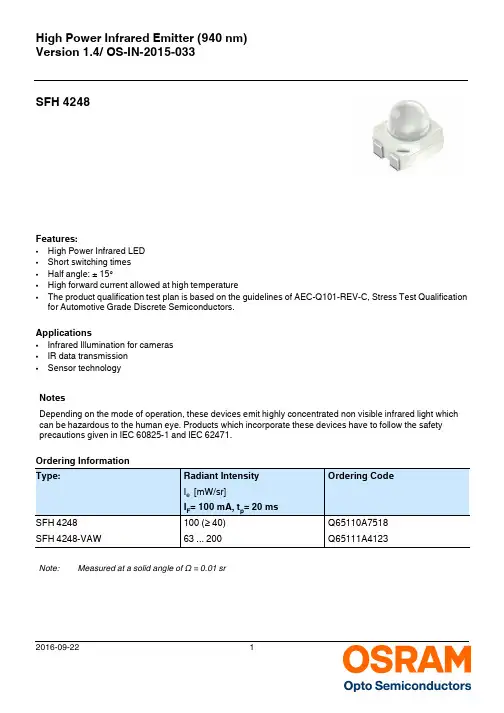
High Power Infrared Emitter (940 nm)Version 1.4/ OS-IN-2015-033SFH 4248Ordering Information Features: •High Power Infrared LED •Short switching times •Half angle: ± 15°•High forward current allowed at high temperature •The product qualification test plan is based on the guidelines of AEC-Q101-REV-C, Stress Test Qualification for Automotive Grade Discrete Semiconductors.Applications •Infrared Illumination for cameras •IR data transmission •Sensor technology NotesDepending on the mode of operation, these devices emit highly concentrated non visible infrared light which can be hazardous to the human eye. Products which incorporate these devices have to follow the safety precautions given in IEC 60825-1 and IEC 62471.Note:Measured at a solid angle of Ω = 0.01 srMaximum Ratings (T= 25 °C)Characteristics (TGrouping (T= 25 °C)Note:measured at a solid angle of Ω = 0.01 srOnly one group in one packing unit (variation lower 2:1).Relative Spectral Emission 3) page 12 I rel = f(λ), T A = 25°CRadiant Intensity 3) page 12I e / I e (100 mA) = f(I F ), single pulse, t p = 25 µs, T A = 25°C8000nm %OHF0413420406080100I λ8509009501025OHF0382110-3mA 101105510-1-2510e e I I F1011021031055(100 mA)Max. Permissible Forward Current I F, max = f(T A ), R thJA = 300 K / WForward Current 3) page 12I F = f(V F ), single pulse, t p = 100 µs, T A = 25°CPermissible Pulse Handling CapabilityI F = f(t p ), T A = 25 °C, duty cycle D = parameterPermissible Pulse Handling CapabilityI F = f(t p ), T A = 85 °C, duty cycle D = parameter00˚C T I mAOHL01716A2040608010012020406080120OHF03822I 10-4V 100A0F-1105510-2-35100.51 1.52 2.521010101010t p1010s 100A I 0.20.40.60.81.01.2t pA I 10101010101010s 2100.10.20.30.40.50.60.70.80.91.1Radiation Characteristics 3) page 12 I rel = f(ϕ)Package OutlineDimensions in mm (inch).OHL0002150˚60˚70˚80˚90˚100˚GPLY6127PinningPackagePower TOPLED with Lens Approximate Weight:37 mgRecommended Solder PadDimensions in mm.Reflow Soldering ProfileProduct complies to MSL Level 2 acc. to JEDEC J-STD-020D.01050100150200250300tT ˚CAll temperatures refer to the center of the package, measured on the top of the component * slope calculation D T/D t: D t max. 5 s; fulfillment for the whole T-rangeTapingDimensions in mm. Tape and Reel12 mm tape with 2000 pcs. on ∅ 180 mm reelTape dimensions [mm]Reel dimensions [mm]Barcode-Product-Label (BPL)Dry Packing Process and MaterialsNote:Moisture-sensitive product is packed in a dry bag containing desiccant and a humidity card.Regarding dry pack you will find further information in the internet. Here you will also find the normative references like JEDEC.OHA04563(G) GROUP:1234567890(1T) LOT NO:(X) PROD NO:123456789LX XXXXRoHS CompliantBIN1: XX-XX-X-XXX-XML X Temp STXXX °C XPack: RXX DEMYX_X123_1234.1234 X 9999(Q)QTY: 4 X_1234.1234 X XX-X-X3_1234X-XX-X- RXX XXXX_X123_123XX-XX-X 234Pack: RX D) D/C:/C:(9D) D 567890NO:123456789torsH NO:123456uctors OptoE XAM PL E678901234(9D) D/C:(6P) BATCH NO:1234567890OSRAM Opto XX-XX-X-X Semiconductors OHA00539Barcode labelTransportation Packing and MaterialsDimensions of transportation box in mmDisclaimerLanguage english will prevail in case of any discrepancies or deviations between the two language wordings. Attention please!The information describes the type of component and shall not be considered as assured characteristics.Terms of delivery and rights to change design reserved. Due to technical requirements components may contain dangerous substances.For information on the types in question please contact our Sales Organization.If printed or downloaded, please find the latest version in the Internet.PackingPlease use the recycling operators known to you. We can also help you – get in touch with your nearest sales office. By agreement we will take packing material back, if it is sorted. You must bear the costs of transport. For packing material that is returned to us unsorted or which we are not obliged to accept, we shall have to invoice you for any costs incurred.Components used in life-support devices or systems must be expressly authorized for such purpose! Critical components* may only be used in life-support devices** or systems with the express written approval of OSRAM OS.*) A critical component is a component used in a life-support device or system whose failure can reasonably be expected to cause the failure of that life-support device or system, or to affect its safety or the effectiveness of that device or system.**) Life support devices or systems are intended (a) to be implanted in the human body, or (b) to support and/or maintain and sustain human life. If they fail, it is reasonable to assume that the health and the life of the user may be endangered.Glossary1)Thermal resistance: junction -ambient, mounted on PC-board (FR4), padsize 16 mm2 each2)Thermal resistance: junction - soldering point, of the device only, mounted on an ideal heatsink (e.g. metal block)3)Typical Values: Due to the special conditions of the manufacturing processes of LED, the typical data or calculated correlations of technical parameters can only reflect statistical figures. These do not necessarily correspond to the actual parameters of each single product, which could differ from the typical data and calculated correlations or the typical characteristic line. If requested, e.g. because of technical improvements, these typ. data will be changed without any further notice.Published by OSRAM Opto Semiconductors GmbHLeibnizstraße 4, D-93055 Regensburg © All Rights Reserved.。
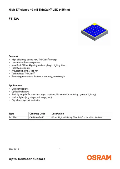
F4152AHigh Efficiency 40 mil ThinGaN ®LED (455nm)2007-09-131Features •High efficiency due to new ThinGaN ® concept •Lambertian Emission pattern•Ideal for LCD backlighting and coupling in light guides •Polarity: n-side up•Wavelength (typ.): 455 nm •Technology: ThinGaN ®•Grouping parameters: luminous intensity, wavelengthApplications •Outdoor displays •Optical indicators•Backlighting (LCD, switches, keys, displays, illuminated advertising, general lighting)•Marker lights (e.g. steps, exit ways, etc.)•Signal and symbol luminaireType Ordering Code DescriptionF4152AQ65110A704040 mil high efficiency ThinGaN ® chip, 450 - 465 nmElectrical values1)(T A = 25 °C)Parameter Symbol Value2)Unitmin.typ.max. Dominant wavelengthI F = 350 mA, pulsedλdom450465nm Reverse voltageI R = 10µAV R10VForward voltageI F = 350 mA, pulsed VF2.73.8VRadiant PowerI F = 350 mA, pulsedΙV32 a.u.1)Measurement limits describe actual settings and do not include measurement uncertainties. Each wafer and fragmentof a wafer is subject to final testing. The wafer or its pieces are individually attached on foils (rings). All el. values are referenced to the vendor's measurement system (correlation to customer product(s) is required). Measurement uncertainty +/-15% for brightness, +/- 1nm for wavelength and +/- 0.1V for voltage.2)Due to the special conditions of the manufacturing processes of LED, the typical data or calculated correlations oftechnical parameters can only reflect statistical figures. These do not necessarily correspond to the actual parameters of each single product, which could differ from the typical data and calculated correlations or the typical characteristic line. If requested, e.g. because of technical improvements, these typ. data will be changed without any further notice.2007-09-1322007-09-133Binning Maximum Ratings 1)Radiant Power 450 - 455 nm455 - 460 nm460 - 465 nm28.0 - 35.2 a.u.A1B1C135.2 - 41.2 a.u.A2B2C241.2 - 48.4 a.u.A3B3C348.4 - 56.8 a.u.A4B4C4> 56.8 a.u.A5B5C5ParameterSymbol Value Unit Maximum Operating temperature range T op -40...+100°C Maximum forward current (T A = 25°C)I F 700mA Minimum forward current (T A = 25°C)I F100mA Maximum surge Current (T A = 25°C)t p = 10 µs, D = 0.05I peak0.7A Maximum junction temperatureT j125°C1)Maximum ratings are strongly package dependent and may differ between different packages. The values given represent the chip in an OSRAM Opto Semiconductor’s Platinum Dragon® package.Mechanical values1)Parameter Symbol Value2)Unitmin.typ.max.Length of chip edge (x-direction)L x0.95 1.00 1.05mm Length of chip edge (y-direction)L y0.95 1.00 1.05mm Diameter of the wafer D50.8mmDie height H170190210µm Diameter of bondpad d130150170µm Additional informationMetallization frontside Gold partialMetallization backside AuDie bonding Epoxy bonding1)All chips are checked according to the following procedure and the OSRAM OS specification of the visual inspectionA63501-Q0013-N001-*-76G3:Unless otherwise described below, the quality level of the final visual inspection shall comply to an AQL 0,4 (according MIL-STD-105D, level II), if the customer performes an incoming visual inspection of a shipment. The quality inspection (final visual inspection) is performed by production. An additional visual inspection step as special release procedure by QM after the final visual inspection is not installed.2)Due to the special conditions of the manufacturing processes of LED, the typical data or calculated correlations oftechnical parameters can only reflect statistical figures. These do not necessarily correspond to the actual parameters of each single product, which could differ from the typical data and calculated correlations or the typical characteristic line. If requested, e.g. because of technical improvements, these typ. data will be changed without any further notice2007-09-1342007-09-135Chip OutlinesDimensions are specified as typicalvalues as follows: mm (inch).Published by OSRAM Opto Semiconductors GmbH Wernerwerkstrasse 2, D-93049 Regensburg © All Rights Reserved.Attention please!The information generally describes the type of component and shall not be considered as assured characteristics or detailed specification.Terms of delivery and rights to change design reserved. Due to technical requirements components may contain dangerous substances. For information on the types in question please contact our sales organization.Handling and Storage Conditions:Storage time for wafers in sealed condition shall not exceed 6 months (storage ambient conditions: Ta=15...30°C;relative humidity: < 60%).The hermetically sealed shipment lot shall be opened under temperature and moisture controlled cleanroom environment only. Customer has to follow the according rules for disposition of material that can be hazardous for humans and environment. Dice have to be handled ESD sensitive.PackingChips are placed on a blue foil with minimum size of 18 x 18 cm².For shipment the wafers of a shipment lot are arranged to stacks. The stack is put in a plastic ESD bag with a maximum of 14 wafers in one bag. A maximum of 4 bags is put in a packaging box. A maximum of 5 packaging boxes is put in a shipping carton which is sealed for storage and shipment.Please use the recycling operators known to you. We can also help you – get in touch with your nearest sales office. By agreement we will take packing material back, if it is sorted. You will have to bear the costs of transport. For packing material that is returned to us unsorted or which we are not obliged to accept, we shall have to invoice you for any costs incurred.Label and shipping documentsEach wafer is identified with a sticker, which is attached to each wafer. The label shows chip type, wafer number, quantity, binning and the minimum, average and maximum values of voltage, luminous intensity and wavelength. Each wafer shipment includes an additional document, which summarizes the content.Design objectives a) workabilityThe chip design was developed and released based on the the vendor’s standard assembly procedures and packaging. Bond strength properties are in accordance to MIL_STD-750D, method 2037. Whether the chip fits to the customer’s product(c) with its according die and wire bond procedures and packaging must be evaluated by the customer himself. If workability problems arise after this release a mutually conducted problem solving procedure has to be set up, if thechips are suspected of contributing to the problemsb) chip characteristicsThe chips are produced by the vendor with best effort, but on chip level a subset of the chip characteristics can be determined only. Performance of the chip in the customer’s product(s) can only be determined by the customer himself. Returns/ComplaintsTo return material because of technical or logistical reasons a RMA-number is necessary. Samples for analysis purposes can be send to OSRAM OS without credit.Shipping Conditions:If not otherwise arranged, the “General Conditions for the supply of products and services of the electrical and electronics industry” apply for any shipment. If these documents are not familiar to you, please request them at our nearest sales office.Components used in life-support devices or systems must be expressly authorized by us for such purpose! Critical components2), may only be used in life-support devices or systems3) with the express written approval of OSRAM OS.1) Typical (refered to as typ.) data are defined as long-term production mean values and are only given for information. This is not a specified value.2)A critical component is a component used in a life-support device or system whose failure can reasonably be expected to cause the failure of that life-support device or system, or to affect its safety or effectiveness of that device or system.3)Life support devices or systems are intended (a) to be implanted in the human body, or (b) to support and/or maintain and sustain human life. If they fail, it is reasonable to assume that the health of the user may be endangered.2007-09-136。
Dimensions: [mm]15detail AScale - 2:1157119B12701Schematic:157119B12701157119B12701157119B12701157119B12701157119B12701157119B12701T e m p e r a t u r eT T T 157119B12701Cautions and Warnings:The following conditions apply to all goods within the product series of Optoelectronic Components of Würth Elektronik eiSos GmbH & Co. KG:General:•This optoelectronic component is designed and manufactured for use in general electronic equipment.•Würth Elektronik must be asked for written approval (following the PPAP procedure) before incorporating the components into any equipment in fields such as military, aerospace, aviation, nuclear control, submarine, transportation (automotive control, train control, ship control), transportation signal, disaster prevention, medical, public information network, etc. where higher safety and reliability are especially required and/or if there is the possibility of direct damage or human injury.•Optoelectronic components that will be used in safety-critical or high-reliability applications, should be pre-evaluated by the customer. •The optoelectronic component is designed and manufactured to be used within the datasheet specified values. If the usage and operation conditions specified in the datasheet are not met, the wire insulation may be damaged or dissolved.•Do not drop or impact the components, the component may be damaged•Würth Elektronik products are qualified according to international standards, which are listed in each product reliability report. Würth Elektronik does not warrant any customer qualified product characteristics beyond Würth Elektroniks’ specifications, for its validity and sustainability over time.•The responsibility for the applicability of the customer specific products and use in a particular customer design is always within the authority of the customer. All technical specifications for standard products also apply to customer specific products.Product specific:Soldering:•The solder profile must comply with the technical product specifications. All other profiles will void the warranty.•All other soldering methods are at the customers’ own risk.Cleaning and Washing:•Washing agents used during the production to clean the customer application might damage or change the characteristics of the optoelectronic component body, marking or plating. Washing agents may have a negative effect on the long-term functionality of the product.•Using a brush during the cleaning process may break the optoelectronic component body. Therefore, we do not recommend using a brush during the PCB cleaning process.Potting:•If the product is potted in the customer application, the potting material might shrink or expand during and after hardening. Shrinking could lead to an incomplete seal, allowing contaminants into the optoelectronic component body, pins or termination. Expansion could damage the components. We recommend a manual inspection after potting to avoid these effects.Storage Conditions:• A storage of Würth Elektronik products for longer than 12 months is not recommended. Within other effects, the terminals may suffer degradation, resulting in bad solderability. Therefore, all products shall be used within the period of 12 months based on the day of shipment.•Do not expose the optoelectronic component to direct sunlight.•The storage conditions in the original packaging are defined according to DIN EN 61760-2.•For a moisture sensitive component, the storage condition in the original packaging is defined according to IPC/JEDEC-J-STD-033. It is also recommended to return the optoelectronic component to the original moisture proof bag and reseal the moisture proof bag again. •The storage conditions stated in the original packaging apply to the storage time and not to the transportation time of the components. Packaging:•The packaging specifications apply only to purchase orders comprising whole packaging units. If the ordered quantity exceeds or is lower than the specified packaging unit, packaging in accordance with the packaging specifications cannot be ensured. Handling:•Violation of the technical product specifications such as exceeding the nominal rated current, will void the warranty.•The product design may influence the automatic optical inspection.•Certain optoelectronic component surfaces consist of soft material. Pressure on the top surface has to be handled carefully to prevent negative influence to the function and reliability of the optoelectronic components.•ESD prevention methods need to be applied for manual handling and processing by machinery.•Resistors for protection are obligatory.•Luminaires in operation may harm human vision or skin on a photo-biological level. Therefore direct light impact shall be avoided. All products are additionally certified as risk groups 0 to 2 according to DIN EN 62471:2008.•In addition to optoelectronic components testing, products incorporating these devices have to comply with the safety precautions given in IEC 60825-1, IEC 62471 and IEC 62778•Please be aware that Products provided in bulk packaging may get bent and might lead to derivations from the mechanical manufacturing tolerances mentioned in our datasheet, which is not considered to be a material defect.Technical specification:•The typical and/or calculated values and graphics of technical parameters can only reflect statistical figures. The actual parameters of each single product, may differ from the typical and/or calculated values or the typical characteristic line.•On each reel, only one bin is sorted and taped. The bin is defined on intensity, chromaticity coordinate or wavelength and forwardWürth Elektronik eiSos GmbH & Co. KGEMC & Inductive SolutionsMax-Eyth-Str. 174638 WaldenburgGermanyCHECKED REVISION DATE (YYYY-MM-DD)GENERAL TOLERANCE PROJECTIONMETHODPLD001.0012023-05-27DIN ISO 2768-1mDESCRIPTIONWL-T7DS 7 Segments Display THTSingle Digit ORDER CODE157119B12701SIZE/TYPE BUSINESS UNIT STATUS PAGEvoltage.•In order to ensure highest availability, the reel binning of standard deliveries can vary. A single bin cannot be ordered. Please contact us in advance, if you need a particular bin sorting before placing your order.•Test conditions are measured at the typical current with pulse duration < 30ms. •Wavelength tolerance under measurement conditions ± 2nm. •Optical intensity tolerance under measurement conditions ±15%. •Forward voltage tolerance under measurement conditions ± 0.2V.These cautions and warnings comply with the state of the scientific and technical knowledge and are believed to be accurate and reliable.However, no responsibility is assumed for inaccuracies or incompleteness.Würth Elektronik eiSos GmbH & Co. KG EMC & Inductive Solutions Max-Eyth-Str. 174638 Waldenburg GermanyCHECKED REVISION DATE (YYYY-MM-DD)GENERAL TOLERANCEPROJECTION METHODPLD001.0012023-05-27DIN ISO 2768-1mDESCRIPTIONWL-T7DS 7 Segments Display THT Single DigitORDER CODE157119B12701SIZE/TYPEBUSINESS UNITSTATUSPAGEImportant NotesThe following conditions apply to all goods within the product range of Würth Elektronik eiSos GmbH & Co. KG:1. General Customer ResponsibilitySome goods within the product range of Würth Elektronik eiSos GmbH & Co. KG contain statements regarding general suitability for certain application areas. These statements about suitability are based on our knowledge and experience of typical requirements concerning the areas, serve as general guidance and cannot be estimated as binding statements about the suitability for a customer application. The responsibility for the applicability and use in a particular customer design is always solely within the authority of the customer. Due to this fact it is up to the customer to evaluate, where appropriate to investigate and decide whether the device with the specific product characteristics described in the product specification is valid and suitable for the respective customer application or not.2. Customer Responsibility related to Specific, in particular Safety-Relevant ApplicationsIt has to be clearly pointed out that the possibility of a malfunction of electronic components or failure before the end of the usual lifetime cannot be completely eliminated in the current state of the art, even if the products are operated within the range of the specifications.In certain customer applications requiring a very high level of safety and especially in customer applications in which the malfunction or failure of an electronic component could endanger human life or health it must be ensured by most advanced technological aid of suitable design of the customer application that no injury or damage is caused to third parties in the event of malfunction or failure of an electronic component. Therefore, customer is cautioned to verify that data sheets are current before placing orders. The current data sheets can be downloaded at .3. Best Care and AttentionAny product-specific notes, cautions and warnings must be strictly observed. Any disregard will result in the loss of warranty.4. Customer Support for Product SpecificationsSome products within the product range may contain substances which are subject to restrictions in certain jurisdictions in order to serve specific technical requirements. Necessary information is available on request. In this case the field sales engineer or the internal sales person in charge should be contacted who will be happy to support in this matter.5. Product R&DDue to constant product improvement product specifications may change from time to time. As a standard reporting procedure of the Product Change Notification (PCN) according to the JEDEC-Standard inform about minor and major changes. In case of further queries regarding the PCN, the field sales engineer or the internal sales person in charge should be contacted. The basic responsibility of the customer as per Section 1 and 2 remains unaffected.6. Product Life CycleDue to technical progress and economical evaluation we also reserve the right to discontinue production and delivery of products. As a standard reporting procedure of the Product Termination Notification (PTN) according to the JEDEC-Standard we will inform at an early stage about inevitable product discontinuance. According to this we cannot guarantee that all products within our product range will always be available. Therefore it needs to be verified with the field sales engineer or the internal sales person in charge about the current product availability expectancy before or when the product for application design-in disposal is considered. The approach named above does not apply in the case of individual agreements deviating from the foregoing for customer-specific products.7. Property RightsAll the rights for contractual products produced by Würth Elektronik eiSos GmbH & Co. KG on the basis of ideas, development contracts as well as models or templates that are subject to copyright, patent or commercial protection supplied to the customer will remain with Würth Elektronik eiSos GmbH & Co. KG. Würth Elektronik eiSos GmbH & Co. KG does not warrant or represent that any license, either expressed or implied, is granted under any patent right, copyright, mask work right, or other intellectual property right relating to any combination, application, or process in which Würth Elektronik eiSos GmbH & Co. KG components or services are used.8. General Terms and ConditionsUnless otherwise agreed in individual contracts, all orders are subject to the current version of the “General Terms and Conditions of Würth Elektronik eiSos Group”, last version available at .Würth Elektronik eiSos GmbH & Co. KGEMC & Inductive SolutionsMax-Eyth-Str. 174638 WaldenburgGermanyTel. +49 (0) 79 42 945 - 0*******************CHECKED REVISION DATE (YYYY-MM-DD)GENERAL TOLERANCE PROJECTIONMETHODPLD001.0012023-05-27DIN ISO 2768-1mDESCRIPTIONWL-T7DS 7 Segments Display THTSingle Digit ORDER CODE157119B12701SIZE/TYPE BUSINESS UNIT STATUS PAGE0.39"eiPal PCN11/11This electronic component has been designed and developed for usage in general electronic equipment only. This product is not authorized for use in equipment where a higher safety standard and reliability standard is especially required or where a failure of the product is reasonably expected to cause severe personal injury or death, unless the parties have executed an agreement specifically governing such use. Moreover Würth Elektronik eiSos GmbH & Co KG products are neither designed nor intended for use in areas such as military, aerospace, aviation, nuclear control, submarine, transportation, transportation signal, disaster prevention, medical, public information network etc.. Würth Elektronik eiSos GmbH & Co KG must be informed about the intent of such usage before the design-in stage. In addition, sufficient reliability evaluation checks for safety must be performed on every electronic component which is used in electrical circuits that require high safety and reliability functions or performance.。
英诺激光科技股份有限公司版权所有不得翻印V3.0目录1、激光器安全 (4)1.1激光等级 (4)1.2激光安全职责 (4)1.3激光安全操作指南 (4)1.4危险及安全标识 (5)1.5AOC 激光器安全特性 (6)1.6保护承诺及政府要求的安全承诺 (6)2、激光器接口说明及随机配件 (7)2.1激光器尺寸 (7)2.2激光器接口说明 (11)2.3随机配件 (11)2.4INTERLOCK 接口 (12)2.5RS232 接口 (12)3、激光器使用要求及注意事项 (13)3.1 电气要求 (13)3.2 工作环境要求 (13)3.3 冷水机要求 (13)3.4 系统安装要求及使用注意事项 (14)4、AOC Ultrafast 激光控制软件安装要求 (15)4.1 软件列表及系统要求 (15)4.2 安装及使用问题解决方法 (15)5、激光系统新一代控制软件界面 (16)5.1 Basic界面说明 (16)5.2 Advanced菜单说明 (17)6、激光器基础操作 (18)6.1 激光器开机顺序 (18)6.2 激光器关机顺序 (20)7、Advanced POD模式简介 (21)8、POD模式下得激光控制方式 (23)8.1 控制方式简介 (23)8.2 控制信号要求 (23)9、激光器故障处理流程 (24)9.1 激光器报警提示及处理方法 (24)9.2 激光器常见故障排除方法 (26)1、激光器安全1.1 激光等级AOC 全系列激光器均属于Class IV 等级激光器(大于500mw),在中国根据GB 7247.1-2012, 同样被列为4 类。
1.2 激光安全职责AOC 全系列激光器是经精心设计并通过严格测试的,以保证其在合理使用条件下是安全可靠的。
如果不按照正确的安全指南进行操作,对人身和财产都是极其危险的,特别当激光的输出波长是裸眼不可见的时候,危险性也随之增加。
若操作人员因为没有按照本司激光器的正常使用规范来使用,由此产生的一切人身伤害,本司不承担任何法律责任。
西班牙兰特钣金软件Lantek2012切割手册给您最好的钣金切割解决方案兰特中国2012-9-1西班牙·兰特钣金软件公司简介西班牙Lantek公司(/cn)是世界著名的钣金行业软件供应商,成立于1986年,总部位于西班牙阿拉瓦高科技园内,离城市Vitoria-Gasteiz 约9公里。
我们专注于为金属板材加工行业提供专业的CAD/CAM和ERP解决方案,我们的软件广泛使用于火焰、等离子、激光、水切割和冲床以及管理信息系统。
25年的发展历史中,我们在全球100多个国家拥有了近万名成功客户。
到现在为止,我们在15个国家设立了分公司:美国,德国,意大利,英国,韩国,法国,西班牙,中国,日本,印度,土耳其,墨西哥,波兰,捷克和阿根廷。
我们的经销商分布全世界:奥地利,澳大利亚,比利时,巴西,加拿大,智利,爱多纳,希腊,荷兰,墨西哥,挪威,葡萄牙,巴拉圭,秘鲁,波兰,俄罗斯,瑞典,新加坡,埃及,委内瑞拉,瑞士等等。
为拓展中国业务,2007年Lantek公司在上海投资成立了兰特克(上海)贸易有限公司,为中国客户提供优质的产品与技术服务。
随着中国业务的迅速发展,目前我们在北京、深圳、武汉各成立了一个办事处,为全国各地的客户,提供迅速便捷的服务。
Lantek钣金的解决方案包括冲、切、折、复合机床编程,三维部件设计和展开、管料和表面切割、折弯编程等。
Lantek在世界范围内和主要厂商长期合作,其中包括LVD、Euromac、Hankwang等。
为方便客户,我们与主流CAD软件供应商合作,包括SolidEdge、SolidWorks、Inventor等。
更多详情,请登录公司网站:目录第一章系统概述 (6)概述 (6)创建任务 (7)载入零件图形 (8)设置和创建钣金 (9)排版 (10)加工 (11)保存和生成切割程序代码 (11)第二章数据库管理 (13)新建数据库 (12)数据备份 (13)数据还原 (14)第三章零件导入及板材管理 (15)零件导入 (15)❝保存部件 (15)❝设置 (17)❝保存设置 (18)❝其他 (19)板材管理 (22)❝新建板材 (22)❝管理板材 (24)❝查找板材 (25)❝输入lst文件 (25)❝创建余材 (26)第四章系统参数 (267)❝职工、货币和税收 (27)❝标识符 (27)❝语言 (28)❝设定:系统 (28)❝设定:绘图和排版 (28)❝设定:成本和花费 (32)❝备用 (33)❝界面 (33)❝打印 (33)第五章机床设置 (34)机床 (34)❝复合割炬设置 (34)❝夹钳设置 (34)1、夹钳位置 (34)3、辅助 (36)❝排除成品器: (39)❝工作区 (40)❝起始点 (40)❝重定位 (41)❝薄板整体参数 (46)系统 (5047)❝数控代码名称 (47)❝余料参数 (49)❝保存选项 (53)❝切割参数 (60)第六章切割工艺设置 (61)❝引入引出线 (61)❝切割断点(微连接) (71)❝转角处理(外绕) (78)❝桥接 (86)❝共边切割 (86)第七章排样模块 (88)结构概述 (88)全做 (89)现有层次作业 (89)一个钣金 (89)一个窗口 (90)单一 (90)删除 (90)移动 (91)干涉 (91)排样模块 (91)栅格 (92)复制 (92)余料 (93)第八章加工模块 (94)自动加工 (94)更改加工 (97)删除加工 (100)重定位 (101)核对加工 (101)显示CNC代码 (102)模拟 (102)后置处理语句 (103)第九章CAD 、报表 (104)CAD模块 (104)第十章后置处理及加密 (115)加密 (115)自动处理 (121)后置文件 (125)第一章系统概述概述Lantek系统专为钣金加工而制作,具有成熟完善的CAD绘图模块、完善的CAM模块和多样的后置处理程序。
《大靶面光学设计:450nm和850nm的应用》一、引言在现代科技领域,光学设计一直扮演着重要的角色。
特别是在大靶面光学设计领域,对于450nm和850nm的应用具有重要意义。
本文将从深度和广度的角度对这一主题进行全面评估。
二、450nm和850nm的概念1. 450nm和850nm的光学波长450nm和850nm分别是两种光学波长的代表,前者属于蓝光波长范围,后者属于红外光波长范围。
2. 光学波长的应用在实际应用中,450nm和850nm的光学波长广泛应用于激光器、光通信、医学成像等领域,具有重要的意义。
三、大靶面光学设计的深度和广度分析1. 大靶面光学设计的原理大靶面光学设计是一种针对大面积光学成像的设计方法,涉及到光学元件的布局、参数调整等方面。
2. 450nm和850nm在大靶面光学设计中的应用针对450nm和850nm的光学波长,在大靶面光学设计中的应用意义和技术难点,是当前研究的热点之一。
四、450nm和850nm在大靶面光学设计中的应用案例1. 450nm和850nm在激光雷达中的应用在激光雷达中,450nm和850nm的光学波长可以实现长距离、高精度的测距和成像,成为大靶面光学设计的重要应用领域。
2. 450nm和850nm在医学成像中的应用在医学成像领域,450nm和850nm的光学波长可以实现非侵入式的生物组织观测和诊断,为大靶面光学设计提供了新的思路和方法。
五、总结与回顾本文从450nm和850nm的概念出发,对大靶面光学设计的深度和广度进行了全面评估。
在实际应用中,450nm和850nm的光学波长在大靶面光学设计中具有重要的应用前景和意义。
作为文章写手,我个人认为450nm和850nm的光学波长将会在未来的光学设计领域中发挥越来越重要的作用。
期待在不久的将来,我们能看到更多基于450nm和850nm的大靶面光学设计应用技术的突破和创新。
六、参考文献1. Smith, J. (2018). Advances in Large-Area and Flexible Electronics. Wiley Online Library.2. Li, Y., & Wang, L. (2020). Optical Design and Testing. Springer.以上就是针对“大靶面光学设计:450nm和850nm的应用”主题的文章,希望对您有所帮助。
G4 50W Demo Laser - Addendum to G4 10-40W Product ManualTable of Contents 1Scope 32Power Supply Requirement 33Mechanical Specification 44Operating Environment 54.1Operating and Storage Conditions 54.2Noise Measurements – 50W S type Demo Laser 55Waveform Reference 65.1Pulse Repetition Rate Ranges 65.2Waveform Reference Tables 7Table of Figures Figure 1.Air Cooled G4 50W – 70W Mechanical Drawing (4)Figure 2.Fan noise measurements – air cooled variants (5)2 G4 50W Demo Laser - Addendum to G4 10-40W Product Manual © 2012 SPI Lasers UK Ltd.1 ScopeThis document covers the G4 50W S type demo lasers. It describes the specific deltas of the 50W demo lasers to the 10 - 40W G4 product family. Therefore, this document should be used in conjunction with the G4 10 - 40W Product Manual, SM-S00245.2 Power Supply RequirementWARNING:supplies and with unspecified control-line states could lead to uncontrolled laser emission with the associated risk of personal exposure to hazardous radiation and product damage.This section details the deltas for the 50W Demo laser modules in term of power supply requirement (Section 11.4 in G4 10-40W Product Manual).The 50W demo lasers are supplied with a 300W Power Supply accessory set up specifically to drive the laser. This has been adjusted to give 26.5V output. This should be used rather than the users own power supplies.Note: On release the 50W G4 laser module will require a 48V supply.4 G4 50W Demo Laser - Addendum to G4 10-40W Product Manual © 2012 SPI Lasers UK Ltd. 3 Mechanical SpecificationThis section details the deltas to section 12 of the G4 10-40W product manual for the 50W, S type G4 laser module.Note : Max height of this G4 Module = 96.5 mm (including paint, the surface finish and labeling)SPI recommend that laser integrators allow suitable clearance on the overall height of the laser to avoid damage/scratching upon installation/removal.Figure 1. Air Cooled G4 50W – 70W Mechanical Drawing3.1.1 G4 Laser Module Weights4 Operating EnvironmentThis section details the deltas to section 13 of the G4 10-40W product Manual for the 50W demo lasers.4.1 Operating and Storage Conditions4.2 Noise Measurements – 50W S type Demo LaserThe measurements for the 50W product were carried out as follows and are shown in the graph below:∙ Made using a GA213 sound pressure meter- 1m from the air intake and outlet of the product ∙ Carried out in a non-anechoic environment – noise floor = 43 dBA so these results are worsethan might be expected when made in an anechoic chamber.The table below summarizes key metrics for a laser running at maximum rated power in thermal equilibrium and quotes the worst case measurements at the air outlet.5 Waveform ReferenceThis section details the deltas to sections 14.1 and 15 of the G4 10 – 40W Product manual for the 50W, S-type demo lasers.5.1 Pulse Repetition Rate RangesNote 1: Limited for 50W demo lasers. Expected to be > 9kW for product release.6 G4 50W Demo Laser - Addendum to G4 10-40W Product Manual © 2012 SPI Lasers UK Ltd.5.2 Waveform Reference Tables。
Areas of applicationPRODUCT DATASHEETENDURA STYLE Lantern Modern 500 12 W DGENDURA® STYLE LANTERN MODERN | Contemporary lanterns with light guide for low-glare illuminationProduct benefitsProduct featuresOutdoor use (IP44)−Building facades−Gardens, balconies and other outdoor areas −Pathway lighting −Driveways−Energy-efficient thanks to LED technology −Easy and quick installation−Very bright and functional outdoor LED luminaires −Die-cast aluminum housing−Available as wall and bollard luminaires−TECHNICAL DATAElectrical dataNominal wattage11.50 W Nominal voltage220…240 V Mains frequency50…60 Hz Nominal current95 mA Power factor λ> 0.5 Protection class I Operating mode Mains voltagePhotometrical dataLuminous flux610 lm Luminous efficacy50 lm/W Color temperature3000 K Light color (designation)Warm White Color rendering index Ra> 80 Standard deviation of color matching≤6 sdcm Flickering metric (Pst LM)-Stroboscope effect metric (SVM)-Beam angle210 °Dimensions & WeightDiameter110.00 mm Height500.00 mm Product weight1900.00 gø110mm500mmMaterials & ColorsProduct color Dark grayHousing color Dark grayBody material AluminumCover material Polycarbonate (PC) Mercury content0.0 mgApplication & MountingAmbient temperature range-20…+40 °C Temperature range at storage-20…+85 °CType of connection Screw terminalType of protection IP44Dimmable NoMounting type SurfaceMounting location WallLED module replaceable Not replaceableLifespanNumber of switching cycles15000Certificates & StandardsStandards CE / EAC / REACH / RoHS Luminaire with limited surface temperature, "D sign"NoEQUIPMENT / ACCESSORIES DOWNLOAD DATADOWNLOAD DATAUser instructionENDURA STYLE LANTERN MODERNTender documentsTender Text 4058075205031Declarations of conformityENDURA STYLE LUMPackaging insertLegal Insert B - Outdoor Not dimmableLOGISTICAL DATAProduct code Packaging unit (Pieces/Unit)Dimensions (length x width x height)Gross weight Volume 4058075205031Folding box1194 mm x 194 mm x 536 mm1998.00 g20.17 dm³4058075205048Shipping box2405 mm x 205 mm x 555 mm4618.00 g46.08 dm³The mentioned product code describes the smallest quantity unit which can be ordered. One shipping unit can contain one or more single products. When placing an order, for the quantity please enter single or multiples of a shipping unit.DISCLAIMERSubject to change without notice. Errors and omission excepted. Always make sure to use the most recent release.Complete mounting and connecting accessories included−。