Flicker Noise 器件参数萃取
- 格式:pdf
- 大小:651.65 KB
- 文档页数:35
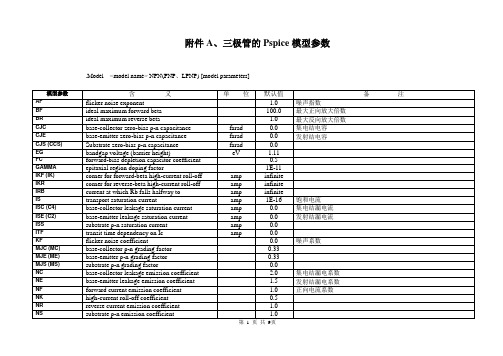
附件A、三极管的Pspice模型参数.Model <model name> NPN(PNP、LPNP) [model parameters]第 2 页共9页附件B、PSpice Goal Function第 3 页共9页附件CModeling voltage-controlled and temperature-dependent resistorsAnalog Behavioral Modeling (ABM) can be used to model a nonlinear resistor through use of Ohm抯 law and tables and expressions which describe resistance. Here are some examples.Voltage-controlled resistorIf a Resistance vs. Voltage curve is available, a look-up table can be used in the ABM expression. This table contains (Voltage, Resistance) pairs picked from points on the curve. The voltage input is nonlinearly mapped from the voltage values in the table to the resistance values. Linear interpolation is used between table values.Let抯 say that points picked from a Resistance vs. Voltage curve are:Voltage ResistanceThe ABM expression for this is shown in Figure 1.第 4 页共9页Figure 1 - Voltage controlled resistor using look-up tableTemperature-dependent resistorA temperature-dependent resistor (or thermistor) can be modeled with a look-up table, or an expression can be used to describe how the resistance varies with temperature. The denominator in the expression in Figure 2 is used to describe common thermistors. The TEMP variable in the expression is the simulation temperature, in Celsius. This is then converted to Kelvin by adding 273.15. This step is necessary to avoid a divide by zero problem in the denominator, when T=0 C.NOTE: TEMP can only be used in ABM expressions (E, G devices).Figure 3 shows the results of a DC sweep of temperature from -40 to 60 C. The y-axis shows the resistance or V(I1:-)/1A.Figure 2 - Temperature controlled resistor第 5 页共9页Figure 3 - PSpice plot of Resistance vs. Temperature (current=1A)Variable Q RLC networkIn most circuits the value of a resistor is fixed during a simulation. While the value can be made to change for a set of simulations by using a Parametric Sweep to move through a fixed sequence of values, a voltage-controlled resistor can be made to change dynamically during a simulation. This is illustrated by the circuit shown in Figure 5, which employs a voltage-controlled resistor.第 6 页共9页Figure 4 - Parameter sweep of control voltageThis circuit employs an external reference component that is sensed. The output impedance equals the value of the control voltage times the reference. Here, we will use Rref, a 50 ohm resistor as our reference. As a result, the output impedance is seen by the circuit as a floating resistor equal to the value of V(Control) times the resistance value of Rref. In our circuit, the control voltage value is stepped from 0.5 volt to 2 volts in 0.5 volt steps, therefore, the resistance between nodes 3 and 0 varies from 25 ohms to 100 ohms in 25 ohm-steps.第7 页共9页Figure 5 - Variable Q RLC circuitA transient analysis of this circuit using a 0.5 ms wide pulse will show how the ringing differs as the Q is varied. Using Probe, we can observe how the ringing varies as the resistance changes. Figure 6 shows the input pulse andthe voltage across the capacitor C1. Comparing the four output waveforms, we can see the most pronounced ringing occurs when the resistor has the lowest value and the Q is greatest. Any signal source can be used to drive the voltage-controlled resistance. If we had used a sinusoidal control source instead of a staircase, the resistance would have varied dynamically during the simulation.第8 页共9页Figure 6 - Output waveforms of variable Q RLC circuit第9 页共9页。

文章编号 :1009 - 2552 (2008) 05 - 0121 - 03中图分类号 : T N773 文献标识码 :A 用于零中频 G PS 接收机的低闪烁噪声混频器彭光宇 , 莫亭亭(上海交通大学微电子学院 , 上海 200240)摘 要 : 设计了一种用于零中频 G PS 接收机的低闪烁噪声混频器 。
通过对吉尔伯特 ( G ilbert ) 混频 器噪声机制的分析 , 以及对 MOS 管偏置在不同区域时噪声性能的研究 , 将吉尔伯特混频器的开关 MOS 管偏置在线性区 , 从而降低其闪烁噪声 。
该电路采用 TS MC 0 . 18μm C MOS 工艺进行了仿 真 , 结果显示 , 改进后的混频器明显降低了低频区域的闪烁噪声 , 而对混频器的其他性能没有影响 。
关键词 : C MOS ; 零中频 ; 混频器 ; 闪烁噪声 ; 热噪声 ; 线性区A lo w flicker noise mixer f o r zero 2IF GPS receiverPE NG G uang 2yu , M O Ting 2ting( Schoo l of Micro electronics , Shangha i Jiaoto ng U niv ersity , S hangha i 200240 , C hina )Abstract : A l ow flicker noise m ixer for z ero 2IF G PS receiver is presented. Based on physical understanding of noise m echanism in G ilbert mixer , as well as the MOSFET noise characteristics in di fferent operating regi ons , the design reduces the flicker noise of the switches in a G ilbert cell by biasing the switches into the linearregi on. The circuit is im plem ented and sim ulated in TS MC 0 . 18μm C MOS technol ogy , the sim ulati on result shows that the proposed mix er reduces the flicker noise obvi ously , without any harm to other perform ance . K ey w or d s : C MOS ; z ero 2IF ; m ixer ; flicker noise ; therm al noise ; linear regi on跨导级 ,开关级和输出负载组成 。

flicker free参数
Flicker free(无闪烁)参数是指在显示器的运行过程中消除或
减少屏幕闪烁的技术和功能。
它可以帮助减少眼睛疲劳和不适,提供更舒适的视觉体验。
使用 flicker free 技术和功能的显示器能够通过调整亮度和刷新率等因素来减少或消除屏幕闪烁。
传统的CRT(阴极射线管)显示器对于眼睛来说可能是有闪烁的,因为它们使用电子束在屏幕上绘制图像,这会引起一定程度的闪烁。
而现代 LCD
(液晶显示)技术通常采用 flicker free 技术,通过控制背光和刷新方式来避免或最小化闪烁。
一些 flicker free 参数包括:
1. 背光技术:一些显示器使用不同的背光技术,如LED(发
光二极管)背光或WLED(白色发光二极管)背光,以提供
更平稳的光照,减少闪烁。
2. 刷新率:液晶显示器的刷新率表示屏幕上的图像更新的频率。
通常,较高的刷新率可以减少或消除闪烁。
常见的刷新率是
60 Hz(每秒60次更新),但某些显示器可以提供更高的刷新率,如120 Hz或更高。
3. PWM调制(脉冲宽度调制):一些显示器使用 PWM 调制
来控制背光亮度。
这种技术会在较低的亮度级别下调整背光的亮度,但会引起一些人的眼睛不适和闪烁感。
flicker free 参数
会包括使用不同的 PWM 调制方式来减少闪烁。
总的来说,flicker free 参数是指显示器使用的技术和功能,用于减少或消除屏幕闪烁,提供更舒适和稳定的视觉体验。


Flicker Free参数1. 什么是Flicker Free参数?Flicker Free参数是指一种用于显示设备的技术参数,旨在消除屏幕闪烁现象。
屏幕闪烁是指在显示器上出现快速、周期性的亮度变化,通常以肉眼难以察觉的频率进行。
这种闪烁会对用户的视觉舒适度和体验产生负面影响。
Flicker Free参数通过调整显示设备的刷新率和亮度控制方式,使屏幕显示稳定、连续、无闪烁。
这意味着用户可以长时间使用设备而不会感到眼睛疲劳或不适。
2. Flicker Free参数的重要性2.1 提升视觉舒适度由于人眼对快速亮度变化敏感,屏幕闪烁可能导致眼睛疲劳、视觉模糊甚至头痛等问题。
Flicker Free参数的应用能够减少这些不适感,提高用户长时间使用显示设备时的视觉舒适度。
2.2 改善阅读和工作效率在长时间阅读或处理文档、电子书籍等工作时,如果屏幕存在闪烁现象,用户的注意力和专注度会受到干扰。
Flicker Free参数的使用可以帮助用户更好地集中注意力,提高工作效率和阅读体验。
2.3 保护视力健康长时间暴露在屏幕闪烁的环境下可能对视力造成损害。
Flicker Free参数通过减少眼睛的疲劳度,降低患眼部不适和视觉问题的风险,有助于保护用户的视力健康。
3. Flicker Free参数的实现方式3.1 调整刷新率显示设备的刷新率是指每秒刷新屏幕图像的次数,通常以赫兹(Hz)为单位表示。
较低的刷新率会增加屏幕闪烁的可能性。
通过提高刷新率,可以使显示设备更接近连续显示图像,从而减少或消除屏幕闪烁。
3.2 使用直流调光(DC Dimming)传统液晶显示器使用脉宽调制(PWM)来控制背光亮度。
这种方式会在调整亮度时引发屏幕闪烁问题。
而直流调光则通过改变背光电压或电流来调整亮度,避免了屏幕闪烁。
3.3 优化背光源背光源是显示设备的重要组成部分,对屏幕闪烁有着直接影响。
使用高质量的背光源可以减少或消除屏幕闪烁现象,提供更稳定、均匀的亮度。
客制化元件模型之參數萃取程作者:台灣安倫科技股份有限公司電子儀器事業群資深應用工程師 許仲延Jackson Hsu一、簡介隨著電子消費產品不斷的推成出新,產品必須多元化才能符合消費者的需求,但是除了產品多元化之外,產品的特性以及穩定性也相當重要。
要達到這基本的要求,就必須要有良好的電路設計技術以提供一個穩定而且準確的電路特性來達到產品的要求。
一般在設計電路時不外乎是利用晶圓代工廠(Foundry) 所提供的元件模型(Device Model) 來模擬含括數十顆或是上百顆元件的複雜電路,而不管在數位或是類比積體電路(IC) 設計都需要主動(Active) 以及被動(Passive) 兩種元件,因此元件模型的建立變成相當的重要。
一個正確建立模型的方法必須要有一定的步驟,如此才能節省不必要的除錯程序以達到事半功倍的效果。
本文將以被動元件電感(Inductor)、電容(Capacitor) 為例,利用安捷倫的IC-CAP 以及ADS/RFDE-Momentum 兩種軟體建立模型。
並且提出有效率的萃取流程(Extraction Flow) 以及方式。
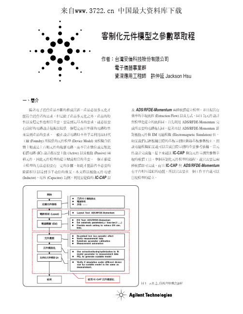
圖1 為元件設計與模型化建立的流程圖,首先利用ADS/RFDE-Momentum 完成所需要的電路佈局圖,接著再以ADS/RFDE-Momentum 針對被動元件做EM 電磁模擬(Electromagnetic Simulation) 值,如果我們已經根據實際的基板量測值做過基板參數校正,則該電磁模擬結果就可以當成實際量測的重要參考依據。
當元件設計完成後,接下來就以IC-CAP 做為元件量測與參數萃取的軟體工具。
整個客制化元件模型的過程,就只需要這兩種軟體即可完成。
而且IC-CAP 與ADS/RFDE-Momentum 有平台相互連結的功能,所以只需要在一個工作平台就可以實現模型的建立。
圖1元件設計與模型化概念流程二、被動元件電路佈局圖A、Substrate 特性的萃取利用ADS/RFDE-Momentum可以完成電路的佈局圖,首先開啟主視窗如圖2 所示,選定Layout 的形狀後就可以在主視窗裡完成佈局圖。
附件A、三极管的Pspice模型参数.Model <model name> NPN(PNP、LPNP) [model parameters]第 1 页共9页第 2 页共9页附件B、PSpice Goal Function第 3 页共9页附件CModeling voltage-controlled and temperature-dependent resistorsAnalog Behavioral Modeling (ABM) can be used to model a nonlinear resistor through use of Ohm抯 law and tables and expressions which describe resistance. Here are some examples.Voltage-controlled resistorIf a Resistance vs. Voltage curve is available, a look-up table can be used in the ABM expression. This table contains (Voltage, Resistance) pairs picked from points on the curve. The voltage input is nonlinearly mapped from the voltage values in the table to the resistance values. Linear interpolation is used between table values.Let抯 say that points picked from a Resistance vs. Voltage curve are:Voltage ResistanceThe ABM expression for this is shown in Figure 1.第 4 页共9页Figure 1 - Voltage controlled resistor using look-up tableTemperature-dependent resistorA temperature-dependent resistor (or thermistor) can be modeled with a look-up table, or an expression can be used to describe how the resistance varies with temperature. The denominator in the expression in Figure 2 is used to describe common thermistors. The TEMP variable in the expression is the simulation temperature, in Celsius. This is then converted to Kelvin by adding 273.15. This step is necessary to avoid a divide by zero problem in the denominator, when T=0 C.NOTE: TEMP can only be used in ABM expressions (E, G devices).Figure 3 shows the results of a DC sweep of temperature from -40 to 60 C. The y-axis shows the resistance or V(I1:-)/1A.Figure 2 - Temperature controlled resistor第 5 页共9页Figure 3 - PSpice plot of Resistance vs. Temperature (current=1A)Variable Q RLC networkIn most circuits the value of a resistor is fixed during a simulation. While the value can be made to change for a set of simulations by using a Parametric Sweep to move through a fixed sequence of values, a voltage-controlled resistor can be made to change dynamically during a simulation. This is illustrated by the circuit shown in Figure 5, which employs a voltage-controlled resistor.第 6 页共9页Figure 4 - Parameter sweep of control voltageThis circuit employs an external reference component that is sensed. The output impedance equals the value of the control voltage times the reference. Here, we will use Rref, a 50 ohm resistor as our reference. As a result, the output impedance is seen by the circuit as a floating resistor equal to the value of V(Control) times the resistance value of Rref. In our circuit, the control voltage value is stepped from 0.5 volt to 2 volts in 0.5 volt steps, therefore, the resistance between nodes 3 and 0 varies from 25 ohms to 100 ohms in 25 ohm-steps.第7 页共9页Figure 5 - Variable Q RLC circuitA transient analysis of this circuit using a 0.5 ms wide pulse will show how the ringing differs as the Q is varied.Using Probe, we can observe how the ringing varies as the resistance changes. Figure 6 shows the input pulse and the voltage across the capacitor C1. Comparing the four output waveforms, we can see the most pronounced ringing occurs when the resistor has the lowest value and the Q is greatest. Any signal source can be used to drive the voltage-controlled resistance. If we had used a sinusoidal control source instead of a staircase, the resistance would have varied dynamically during the simulation.第8 页共9页Figure 6 - Output waveforms of variable Q RLC circuit第9 页共9页。
第10章习题参考答案
1.答、热噪声(Thermal Noise):也就是约翰逊噪声(Johnson Noise)或白色噪声(White Noise),这种噪声敏感于温度的变化,由导体中的自由电子和振动粒子之间的热量的相互作用而产生,它的频率在频谱总均匀分布。
散粒噪声(Shot Noise):这种噪声是由各种形式半导体中载流子的分散特性而产生的,这种噪声为晶体管的主要噪声。
闪烁噪声(Flicker Noise):又称为超越噪声(Excess Noise)、粉红噪声(Pink Noise)或1/f噪声,通常由双极型晶体管(BJT)和场效应管(FET)产生,且发生在频率小于1kHz 以下。
闪烁噪声是所有线性器件固有的随机噪声,噪声振幅与频率成反比,频率很低时这种噪声较大,频率较高时(几百赫兹以上)这种噪声的影响较小。
在电路的输入端,闪烁噪声通常是频率低于400Hz时的主要噪声源。
2答:失真分析(Distortion Analysis)用于分析电子电路中的非线性失真和相位偏移,通常非线性失真会导致谐波失真,而相位偏移会导致互调失真。
3、建立10-44仿真电路
对该电路进行静态工作点分析的结果如下图10.1所示。
图10.1
对6节点进行交流分析的结果如下图10.2所示。
图10.2
对节点6进行瞬态分析的结果如下图10.3所示,其中End time(TSTOP)设置为0.1s。
图10.3。
·1259·低相噪、高集成度频率源的研制周文衎 童 超 王晓江(南京电子设备研究所,南京 210007)zhouwenkan1314@摘 要:本文介绍了一种低杂散、低相噪、高集成度的频率源的研制。
该频率源采用Hittite 公司的鉴相器HMC830LP6G ,通过锁相产生1GHz 信号,杂散抑制≥70dBc 、相噪达到-116dBc/Hz@1kHz 。
由于鉴相器内部集成VCO ,所有器件布局在50×20mm 的范围内,大大减少了电路板的面积,提高了设计的集成度,实现了小型化。
关键词:低杂散,低相噪,HMC830,高集成度Design of Low Phase Noise and High Integration Frequency SynthesizerZHOU wenkan, TONG chao,WANG xiaojiang(Nanjing Electronic Equipment Institute, Nanjing 210007)Abstract: In this paper, a frequency synthesizer with low spurious and phase noise is presented. In this design we implement phase detector HMC830LP6G of Hittite to generate a signal of 1GHz,the spurious is below -70dBc and phase noise reach a level of -116dBc/Hz@1kHz.As VCO is inner integrated ,all components can be arranged in a area of 50×20mm,so the PCB is highly integrated, and make minimization possible. Keywords: Low spurious, Low phase noise, HMC830, High Integration1 引言HMC830是Hittite 公司推出的一款鉴相器,内部集成了VCO 以及分频器,支持小数、整数两种模式,可输出25MHz 到3000MHz 信号,鉴相频率最高可到100MHz 。
CMOS VCO设计综述摘要:本文从相位噪声理论的发展和主流低噪声设计技术两个方面,阐述了CMOS VCO 的发展现状和未来的趋势。
在理论方面,从线性时不变模型到线性时变模型的发展成功的解释了低频噪声和高频谐波噪声转变为相位噪声的物理机理,为CMOS VCO的低噪声设计提供了理论依据和指导。
而随着理论的发展,新的优化技术也不断出现,例如高Q值电感设计技术,互补型结构,对称性设计,尾电流管滤波技术,Harmonic Tuning技术,Back to Back V aractor,AAC技术等等。
本文详细阐述了这些技术的优势和局限性,指出了未来的发展方向。
一.前沿无线通信的广泛应用和半导体工业的迅速发展使得全集成发射接收机(Transeiver)的设计成为一个重要的研究领域[1-7]。
在Transceiver中,压控振荡器是一个非常关键的模块,其位置如图1所示:图1. 接收机原理图由图1可以看出:VCO和鉴相器/电荷泵(PFD/CP),分频器(Divider)以及晶振(Xtal)一起构成了频率综合器,为混频器提供本振信号,实现对输入RF信号的频率搬移,如图2(a)所示:图2 (a)理想本振信号下频率搬移示意图;(b)带相位噪声本振信号下的频率搬移示意图图2(a)给出的是本振为理想信号情况下的频率搬移示意图,此时本振在频谱上表现为一个脉冲。
但是由于器件噪声等非理想因素,真实的本振信号在频率上表现为一个窄带信号(Skirts),如图2(b)所示。
这样,当所要信号附近有一个强干扰信号时,干扰信号就可能通过本振信号的边带搬移到中频处,从而干扰所要信号的正常接受。
表现在接受机性能上,就是会降低选择型(selectivity)和敏感度(Sensitivity)[8]。
设计人员习惯用相位噪声(Phase Noise)来表征本振信号边带的大小(第二节会详述),因此降低本振信号的相位噪声成为提高接受机性能的关键。
频率综合器的各个模块包括VCO,Xtal,PFD/CP以及Divider都会引入噪声源影响本振信号的相位噪声,但是由于噪声引入位置的不同,对于Xtal,PFD/CP,Divider 处的噪声PLL表现出低通特性而对于VCO的噪声PLL表现出高通特性[16]。