KT6008-1A升压型DC-DC芯片
- 格式:pdf
- 大小:1.29 MB
- 文档页数:13

手机万能学习红外遥控IC概述DC6008是一款高性能、高集成、低成本、低功耗的手机万能学习红外遥控IC,同时具备强大的红外万能遥控器和红外学习遥控器的功能。
手机主芯片可以通过GPIO口与DC6008进行通信。
DC6008适用场合:手机(功能机或智能机)或MID等。
功能特点¾工作电压范围为2.0V到3.6V¾静态电流2.0µA以下¾内置IR_LED发射驱动管和学习放大电路¾外围电路极其简单上电复位¾低电压检测 1.6V¾封装DFN8(3mm×3mm)管脚排列图管脚说明名称 方向 管脚 说明SCK I 1时钟口(接主片GPIO) NC 2保留,布板时悬空NC 3保留,布板时悬空BUSY O 4芯片状态指示(接主片GPIO)RMT I/O 5红外发射和学习口VDD 6电源GND 7地SDA I/O 8数据口(输出为开漏)(接主片GPIO)应用说明手机主芯片可以通过SCK/SDA/BUSY端口与DC6008进行通信,在发射时可将手机中存储的万能数据库(包括电视/机顶盒/DVD/空调/风扇等)通过SCK/SDA/BUSY端口送到DC6008进行编码和调制后通过红外管发射出去遥控电器;也可以学习和还原发射市面上几乎所有编码格式的遥控器,可学习的红外载波频率范围可覆盖0~85KHz,可以支持电视机、机顶盒、空调、DVD、电风扇、投影器等遥控设备的发射。
(空调码属于智能码,码值实时变化,暂时不能学习)手机对DC6008的操控由手机APP软件来完成。
APP软件以及万能遥控数据库由用户进行定制。
整机应用指标说明:¾反应灵敏,遥控速度快捷,按键到电器响应结果小于0.5秒。
¾使用普通的红外发光二极管发射距离大于10米。
¾在0~2cm距离内可进行稳定可靠的学习,一次性学习成功率大于95%以上。
典型应用图典型应用电路如图2所示。

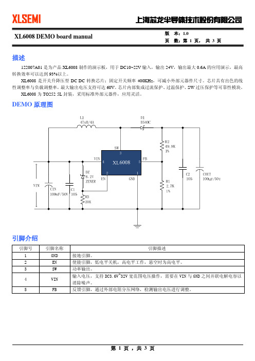
页 数:第 1 页, 共 3 页描述122007A01是为产品XL6008制作的演示板,用于DC10~22V 输入,输出24V ,输出最大0.6A 的应用演示,最高转换效率可以达到93%以上。
XL6008是开关升降压型DC-DC 转换芯片;固定开关频率400KHz ,可减小外部元器件尺寸。
芯片具有出色的线性调整率与负载调整率,最大输出电压支持可达60V 。
芯片内部集成过流保护、过温保护、SW 过压保护等可靠性模块。
XL6008为TO252-5L 封装,采用标准外部元器件,应用灵活。
DEMO 原理图引脚介绍引脚号 引脚名称 引脚描述1 GND 接地引脚。
2 EN 使能引脚,低电平关机,高电平工作,悬空时为高电平。
3 SW 功率输出。
4 VIN 输入电压,支持DC3.6V~32V 宽范围电压操作,需要在VIN 与GND 之间并联电解电容以消除噪声。
5 FB反馈引脚,通过外部电阻分压网络,检测输出电压进行调整。
页 数:第 2 页, 共 3 页物料清单序号 数量 参考序号描述料号 生产商 1 1 C1 1uF,50V,Ceramic,X7R,0805 C2012X7R1H105K TDK 2 1 C2 1uF,50V,Ceramic,X7R,0805 C2012X7R1H105K TDK 3 1 CIN 100uF,50V,Electrolytic,(8x11.5) YXJ-50V-100uF Rubycon 4 1 COUT 100uF,50V,Electrolytic,(8x11.5) YXJ-50V-100uFRubycon 5 1 D1 40V,5A,Schottky Barrier Rectifier,SMCB540C DIODES 6 1 DZ 8.2V,500mW,ZENER,MINI MELF TCBZV55C 8V2TAK CHEONG7 1 L1 47uH,4A,Toroidal,18*9 CS127125-T29 8 1 R1 2.7KΩ,1%,1/16W,Thick Film,0603 RL0603xR-072701L Yageo 9 1 R2 49.9KΩ,1%,1/16W,Thick Film,0603 RL0603xR-074992L Yageo 10 1 R3 20KΩ,1%,1/16W,Thick Film,0603 RL0603xR-072002LYageo 111U160V,400KHz,BOOST DC-DC Converter,TO252-5LXL6008XLSEMI性能数据转换效率: 负载调整率:Efficiency VS Output currentOutput voltage VS Output current页数:第 3 页,共3 页DEMO实物图PCB布局底层PCB布局指南1.VIN、GND、SW、VOUT等功率线,粗、短、直;2.FB走线远离电感与肖特基等开关信号地方,建议使用地线包围;3.输入电容靠近芯片VIN与GND引脚。
V2.2目录第1章安装使用 _________________________________________________ 1-11.1使用注意事项___________________________________________________________________ 1-11.2移动时的注意要点________________________________________________________________ 1-11.3连接交流电源线__________________________________________________________________ 1-21.4接地___________________________________________________________________________ 1-21.5操作检查_______________________________________________________________________ 1-31.6仪器的其它特性__________________________________________________________________ 1-3 第2章操作规范和措施 ___________________________________________ 2-12.1禁止的操作行为__________________________________________________________________ 2-12.2紧急情况的处理__________________________________________________________________ 2-12.3测试中的预防措施________________________________________________________________ 2-12.4高压测试警告___________________________________________________________________ 2-22.5有故障仪器的危险状态处理________________________________________________________ 2-32.6保证长时间无故障使用的条件______________________________________________________ 2-32.7日常检查_______________________________________________________________________ 2-3 第3章仪器面板概述 _____________________________________________ 3-13.1前面板说明_____________________________________________________________________ 3-13.1.1电源开关(POWER) _____________________________________________ 3-13.1.2 START键、STOP键 ___________________________________________ 3-13.1.3商标及型号___________________________________________________ 3-13.1.4 USB接口 ____________________________________________________ 3-13.1.5指示灯区域___________________________________________________ 3-13.1.6功能区域(FUNCTION) _______________________________________ 3-13.1.7 HV __________________________________________________________ 3-23.1.8输出电压高端(HV) __________________________________________ 3-23.1.9测试低端、测试电流返回端(LOW /RET) ___________________________ 3-23.1.10移动键______________________________________________________ 3-23.1.11快捷功能键 __________________________________________________ 3-23.1.12 COPY键 ____________________________________________________ 3-23.1.13 LCD液晶显示屏 _____________________________________________ 3-23.2后面板说明_____________________________________________________________________ 3-33.2.1功放风扇散热口_______________________________________________ 3-33.2.2测试低端、测试电流返回端(选件) _____________________________ 3-33.2.3高压输出端(选件)___________________________________________ 3-33.2.4电源插座:自带保险丝盒,可切换线电压模式。
1.5MHz, 500mA STEP-UP DC-DC CONVERTERFigure 1. Package Type of KT6860The KT6860 is available in The KT6860 has built-in overvoltage protection (OVP)The KT6860 is a high power, constant frequency, cur-Aug.0601General Descriptionrent mode PWM, inductor based, step-up (boost) con-verter. The converter operates at high frequency(1.5MHz) so that a small, low profile inductor can be used.to allow the device goes into shutdown mode when the output voltage exceeds the OVP threshold of 29V .standard SOT-23-5 pack-age.Features·High Efficiency up to 81%·Adjustable Output V oltage up to 29V ·Shutdown Current 1µA Typical · 1.5MHz Switching Frequency·36V 500mA Rugged Integrated Bipolar Switch ·Built-in Soft-start to Reduce Inrush Current Dur-ing Start-up·On-chip Overvoltage Protection·Uses Low ESR Ceramic Output Capacitor ·Uses Small InductorApplications·LCD/OLED Display Bias Supply·White LED Driver for LCD Display Backlights ·Cellular PhonesSOT-23-5208Rev.1.4KT68Figure 2. Pin Configuration of KT6860 (Top View)2Pin DescriptionPin NumberPin Name Function1SWSwitch Pin. Connect inductor/diode here. The output voltage can go up to 29V but should not exceed this limit. If the voltage on this pin is higher than the overvoltage protection (OVP)threshold, the device can go into shutdown mode. It can be restarted by a low to high pulse on the SHDN pin, or by a power on reset on the V IN supply 2GND Ground Pin. Connect directly to local ground plane3FBFeedback Pin. Internally compares to 1.25V . Connect R1 and R2 resistor divider here. Calcu-late the Output V oltage according to the formula: V OUT =1.25V * (1+R1/R2)4SHDN Shutdown Pin. Connect to 1.5V or higher to enable device (ON), 0.4V or lower to disabledevice (OFF)5V INInput Supply Pin. Must be locally bypassedPin ConfigurationK Package(SOT-23-5)SW FBV INSHDNGND Aug.060208Rev.1.4KT 68Figure 12. LCD/OLED Display Bias Driver Typical CircuitNote: V OUT =1.25*(1+R1/R2)=1.25*19.2=24VC: X5R or X7R DielectricL: SUMIDA CDTH3D14/HPNP-100NC or Equivalent3Functional Block DiagramFB SHDNV INAug.060208Rev.1.4KT 68number, are RoHS compliant. Products with KT6860KTRP KT6860KTRG E6BG Tape & ReelLead FreeOrdering InformationPackageTemperature RangePart NumberMarking IDPacking TypeLead FreeGreenLead FreeGreenSOT-23-5-40 to 85o CK: SOT-23-5G: GreenTR: Tape & ReelPackage TypeP"G" suffix are available in green packages.signated with "P" suffix in the part KINETEIC's Pb-free products, as de4Aug.0208Rev.1.4Note 1: Stresses greater than those listed under "Absolute Maximum Ratings" may cause permanent damage to the device. These are stress ratings only, and functional operation of the device at these or any other conditions beyond those indicated under "Recommended Operating Conditions" is not implied. Exposure to "Absolute Max-imum Ratings" for extended periods may affect device reliability.Parameter Symbol Min Max Unit Input V oltage V IN 2.616VOperating TemperatureT OP-4085oCRecommended Operating ConditionsAbsolute Maximum Ratings (Note 1)Parameter Symbol Value Unit Input V oltage V IN20V SW V oltage 38V FB V oltage 5V SHDN V oltage16VThermal Resistance (Junction to Atmosphere, no Heat sink) R θJA265oC/WOperating Junction Temperature 150o C Storage Temperature Range T STG -65 to 150o C Lead Temperature (Soldering, 10sec)T LEAD260oCESD (Machine Model)250V ESD (Human Body Model)2000VElectrical Characteristics(V IN=3V, V SHDN=3V, T A=25o C, unless otherwise specified.)Parameter Symbol Conditions Min Typ Max Unit2.6VMinimum Operating V olt-age16V Maximum Operating V olt-ageFeedback V oltage V FB V IN=5V, V OUT=24V, I OUT=30mA 1.17 1.25 1.33VFB Pin Bias Current V FB=1.25V1045100nASupply Current I CC V SHDN =V FB=V IN, No switching 2.5 3.5mASupply Current I Q V SHDN =0V, V FB=0V0.1 1.0µASwitching Frequency f 1.1 1.5 1.9MHzMaximum Duty Cycle D MAX8590%Switching Current Limit Duty Cycle=80%500mASwitch VCESAT V CESAT I SW=250mA300mVSwitch Leakage Current V SW=5V0.015µASHDN V oltage High (ON)V TH 1.5V SHDN V oltage Low (OFF)V TL0.4SHDN Pin Bias Current55µAOVP V oltage Threshold V OVP29VSoft-Start Time550µS5 Aug.06Aug.0208Rev.1.4Typical Performance CharacteristicsFigure 4. Quiescent Current vs. Input Voltage Figure 5. SHDN Pin Bias CurrentFigure 6. Switching Frequency Figure 7. Feedback Bias Current-50-2502550751000.00.40.81.21.62.0S w i t c h i n g F r e q u e n c y (M H z )Junction Temperature (oC)Junction Temperature (oC)vs. Junction Temperaturevs. Junction Temperaturevs. Junction Temperature7Aug.0208Rev.1.4Figure 9. Switching Current Limit vs. Duty CycleTypical Performance Characteristics (Continued)Figure 10. Feedback Voltage vs. Junction Temperature Figure 11. Efficiency vs. Output CurrentFigure 8. Efficiency vs. Junction Temperature1.241.251.261.271.281.29F e e d b a c k V o l t a g e(V )8Aug.0208Rev.1.4SOT-23-5Unit: mm(inch)Mechanical Dimensions0.000(0.000)1.050(0.041)9)0.100(0.004)。
n Built in Thermal Shutdown Functionn Built in Current Limit Functionn Available in TO252-5L packageApplicationsn Automotive and Industrial Boost /Buck-Boost / Inverting Convertersn Portable Electronic EquipmentFigure1. Package Type of XL6008Pin ConfigurationsFigure2. Pin Configuration of XL6008 (Top View) Table 1 Pin DescriptionPin Number Pin Name Description1 GND Ground Pin.2 EN Enable Pin. Drive EN pin low to turn off the device, drive it high to turn it on. Floating is default high.3 SW Power Switch Output Pin (SW).4 VIN Supply V oltage Input Pin. XL6008 operates from a 3.6V to 32V DC voltage. Bypass Vin to GND with a suitably large capacitor to eliminate noise on the input.5 FB Feedback Pin (FB). The feedback threshold voltage is 1.25V.Function BlockFigure3. Function Block Diagram of XL6008 Typical Application CircuitFigure4. XL6008 Typical Application Circuit (Boost Converter)to the device. This is a stress rating only and functional operation of the device at these or any other conditions above those indicated in the operation is not implied. Exposure to absolute maximum rating conditions for extended periods may affect reliability.XL6008 Electrical CharacteristicsT a = 25℃;unless otherwise specified.Symbol Parameter Test Condition Min. Typ. Max. Unit System parameters test circuit figure4VFB FeedbackV oltageVin = 12V to 16V, V out=18VIload=0.1A to 1A1.213 1.25 1.287 VEfficiency ŋVin=12V ,V out=18.5VIout=1A- 92 - %Electrical Characteristics (DC Parameters)Vin = 12V, GND=0V, Vin & GND parallel connect a 220uf/50V capacitor; Iout=0.5A, T a = 25℃; the others floating unless otherwise specified.Parameters Symbol Test Condition Min. Typ. Max. Unit Input operation voltage Vin 3.6 32 V Shutdown Supply Current I STBY V EN=0V 70 100 uAQuiescent Supply Current I q V EN =2V,V FB =Vin2.5 5 mAOscillator Frequency Fosc 320 400 480 Khz Switch Current Limit I L V FB =0 3 AOutput Power NMOS Rdson Vin=12V,I SW=3A110 120 mohmEN Pin Threshold V EN High (Regulator ON)Low (Regulator OFF)1.40.8VI H V EN =2V (ON) 3 10 uA EN Pin Input LeakageCurrent ILV EN =0V (OFF) 3 10 uA Max. Duty Cycle D MAX V FB=0V 90 %Typical System Application – Boost (Output 18.5V/1A)Figure5. XL6008 Typical System Application (Boost Converter)Typical System Application – SEPIC Buck-Boost (Input 10V~30V, Output 12V/2A)Figure6. XL6008 Typical System Application (SEPIC Buck-Boost Converter) Typical System Application for Inverting Converter– SEPIC Inverting Topology (Input 10V~30V, Output + -12V/0.6A)Figure7. XL6008 Typical System Application (SEPIC Inverting Converter)Package Information TO252-5L。
选型表认证产品型号输入电压(VDC)输出效率(%/Typ.)(最小Vin)/(最大Vin)@满载最大容性负载(µF)标称值(范围值)输出电压(VDC)最大输出电流(mA)UL/CE/CB (认证中)K7803M-1000R324(6-36) 3.3100090/80680K7805M-1000R324(8-36)5100093/8568012(8-27)-5-50085/81330K7809M-1000R324(13-36)9100094/89680K7812M-1000R324(16-36)12100095/9268012(8-20)-12-30088/87330K7815M-1000R324(20-36)15100096/9368012(8-18)-15-30087/88330注:当输入电压超过30VDC 时,输入端需外接22µF/50V 的电解电容,以防电压尖峰造成模块损坏。
输入特性项目工作条件Min.Typ.Max.单位空载输入电流正输出--0.31mA负输出--14反接输入禁止输入滤波器类型电容滤波输出特性项目工作条件Min.Typ.Max.单位输出电压精度满载,输入电压范围K7803M-1000R3--±2±4%其他型号--±1.5±3线性调节率满载,输入电压范围--±0.2±0.4负载调节率标称输入电压,10%-100%负载正输出--±0.4±0.6负输出--±0.4±0.8纹波&噪声*20MHz 带宽,标称输入电压,20%-100%负载--2575mVp-p 温度漂移系数100%负载----±0.03%/℃瞬态响应偏差标称输入电压,25%-50%-25%、50%-75%-50%负载阶跃变化--±60±200mV宽电压输入,非隔离稳压单路输出专利保护RoHS产品特点●效率高达96%●空载输入电流低至0.3mA●工作温度范围:-40℃to +85℃●支持负输出●短路保护●引脚与LM78xx 系列兼容●满足UL62368,EN62368,IEC62368认证(认证中)K78xxM-1000R3系列是高效率的开关稳压器,是LM78xx 系列三端线性稳压器的理想替代品。