YY1002_DC-DC 升压IC中文版
- 格式:pdf
- 大小:969.29 KB
- 文档页数:12

DC-DC输出可调开关电源摘要本系统为DC-DC升降压变换器,由CPU最小系统模块、供电模块、升压模块、降压模块、液晶显示模块和辅助电路六部分组成。
选用SMT32F103作为主控制器,采用降压芯片LM2596-ADJ作为实现降压,将AD采集的输出电压和电流与预设值比较,然后通过DA调节输出电压电流,对于降压模式的下恒流或恒压工作状态也可通过按键进行切换,同时调节按键可实现输出电压或电流大小的变换;升压模块采用了LM2577-ADJ,手动滑动变阻器的阻值可调节输出电压;加入液晶显示系统工作模式和输出电压、电流;对于升降压的切换也可通过按键切换;供电电源提供了3.3V和12V,分别为CPU、液晶和运放偏置供电;辅助电路方便开发者的调试。
最终系统能够在手动切换工作模式的情况下输出预设的电压和电流,并显示出来。
关键词:DC-DC 升降压可调abstractThe system for the DC-DC buck converter, the minimum system CPU module, power supply module, boost module, step-down module, LCD display module and the auxiliary circuit six parts. SMT32F103 chosen as the main controller, buck chip LM2596-ADJ as enabling buck, the AD acquisition of output voltage and current compared with the preset value, then adjust the output voltage and current through the DA, the constant current mode buck or constant work status can also be switched through the button while adjusting key enables the size of the output voltage or current transformation; step-up module uses the LM2577-ADJ, manual sliding rheostat resistance adjustable output voltage; added liquid crystal display system working mode and the output voltage and current; the buck switch can also be switched by key; providing a 3.3V power supply and 12V, respectively, CPU, LCD bias supply and the op amp; facilitate the development of the secondary circuit debugging. Final system can output a preset voltage and current in the case of manual operating mode switch, and displayed.Key words:DC-DC Boosted、Reduce voltage Adjustable目录第一章绪论 (1)1.1 开关电源概述 (1)1.2 开关电源与线性电源比较 (1)1.3 开关电源发展趋势与应用 (1)第二章系统功能介绍 (2)第三章系统方案选取与框图 (3)3.1 系统整体框图 (3)3.2 系统方案选取 (3)第四章硬件电路设计 (6)4.1 主控制器 (6)4.2 供电模块 (7)4.3 降压模块电路设计 (8)4.4 升压模块电路设计 (10)4.5 液晶显示电路 (13)五硬件开发环境 (14)5.1 Altium Designer 09 (14)5.2 电源设计软件SwitchPro (14)5.3 电路板雕刻机LPKF ProtoMat E33 (15)675.4 电镀机LPKF MiniLPS (17)5.5 SMD精密无铅回焊炉ZB-2518H (17)第六章软件设计框图 (20)第七章系统调试 (21)参考文献 (22)总结致谢 (23)附录 (24)第一章绪论1.1 开关电源概述我们身边使用的任何一款电子设备都离不开它可靠的电源,计算机电源全面实现开关电源化于80年代,并率先完成计算机的电源更新换代,进入90年代,开关电源开始进入各种电子、电气设备领域,程控交换机、通讯、电子检测设备电源、控制设备电源等都已大面积使用了开关电源,更加促进了开关电源技术的迅猛发展。


PYBJ15-Q24-S5-Mdate 06/24/2019page1 of 9SERIES: PYBJ15 │ DESCRIPTION: DC-DC CONVERTERFEATURES• up to 15 W isolated output• ultra wide 4:1 input voltage range • single regulated output• output short circuit, over current, over voltage protection • efficiency up to 89%• DIP and SMT mounting styles • available with or without case• 1500 Vdc isolationMODELinput voltageoutput voltageoutput currentoutput powerripple & noise 1efficiency 2typ (Vdc)range (Vdc)(Vdc)min (mA)max (mA)max (W)max (mVp-p)typ (%)PYBJ15-Q24-S3249~36 3.30450014.8510088PYBJ15-Q24-S5249~365030001510088PYBJ15-Q24-S12249~3612012501510089PYBJ15-Q24-S15249~3615010001510089PYBJ15-Q48-S34818~75 3.30450014.8510088PYBJ15-Q48-S54818~755030001510088PYBJ15-Q48-S124818~7512012501510089PYBJ15-Q48-S154818~751510001510089Notes: 1. From 5~100% load, nominal input, 20 MHz bandwidth oscilloscope, with 10 µF tantalum and 1 µF ceramic capacitors on the output. From 0~5% load, ripple and noise is <5% Vo.2. Measured at nominal input voltage, full load.3. All specifications are measured at T a=25°C, humidity < 75%, nominal input voltage, and rated output load unless otherwise specified.PART NUMBER KEYBase NumberPYBJ15 - Q XX - S XX - X XInput VoltageOutput VoltageCase:“blank” = with case O = no caseMounting Style:D = DIPM = SMTdate 06/24/2019 │page 2 of 9 CUI Inc │ SERIES: PYBJ15 │DESCRIPTION: DC-DC CONVERTERINPUTparameter conditions/description min typ max unitsoperating input voltage24 Vdc input models48 Vdc input models 91824483675VdcVdcstart-up voltage24 Vdc input models48 Vdc input models 918VdcVdcsurge voltage24 Vdc input models for 1 second max48 Vdc input models for 1 second max -0.7-0.750100VdcVdcunder voltage shutdown24 Vdc input models48 Vdc input models 5.5126.515.5VdcVdccurrent 24 Vdc input models3, 5 Vdc output models12, 15 Vdc output models727718mAmA48 Vdc input models 3.3 Vdc output models5 Vdc output models363360mAmAstart-up current24 Vdc input models48 Vdc input models 3,0001,500mAmAremote on/off (CTRL)4turn on (CTRL pin pulled low to GND (0~1.2 Vdc))turn off (CTRL pin open or pulled high (3.5~12 Vdc))input current when switched off615mAalarm indication (ALM)Valm (relative to GND), when under voltage protection isgoing to happen, and during the over voltage protectionworking status.0.2 1.2Vdc Valm (relative to GND), other working status 3.59Vdcfilter Pi filterno load power consumption0.36W Notes: 4. The voltage of the CTRL pin is referenced to input GND pin.OUTPUTparameter conditions/description min typ max unitsmaximum capacitive load53.3, 5 Vdc output models12 Vdc output models15 Vdc output models4,7001,000820μFμFμFvoltage accuracy from 0% to full load±1±2% line regulation from low line to high line, full load±0.2±0.5% load regulation6from 5% to full load±0.5±1% switching frequency7PWM mode300kHz transient recovery time25% load step change, nominal input voltage300500μstransient response deviation 25% load step change, nominal input voltage3.3, 5 Vdc output modelsall other output models±3±3±8±5%%temperature coefficient at full load±0.03%/°C Note: 5. Tested at input voltage range and full load.6. At 0~100% load, the max load regulation is ±3%.7. Value is based on full load. At loads <50%, the switching frequency decreases with decreasing load for efficiency improvement.date 06/24/2019 │ page 3 of 9CUI Inc │ SERIES: PYBJ15 │ DESCRIPTION: DC-DC CONVERTER PROTECTIONSparameterconditions/description min typmax units over voltage protection output shut down 110160%over current protection hiccup, auto recovery110180230%short circuit protectionhiccup, continuous, auto recoverySAFETY AND COMPLIANCEparameter conditions/descriptionmin typ max units isolation voltageinput to output for 1 minute at 1 mA input to case 8 for 1 minute at 1 mA output to case 8 for 1 minute at 1 mA 1,500500500Vdc Vdc Vdc isolation resistance input to output at 500 Vdc input to case 8 at 500 Vdc output to case 8 at 500 Vdc 100100100MΩMΩMΩisolation capacitance input to output, 100 kHz / 0.1 V 1,000pFsafety approvals IEC 62368-1, EN 62368-1conducted emissions CISPR32/EN55032, class B (external circuit required, see Figure 2-a) radiated emissions CISPR32/EN55032, class B (external circuit required, see Figure 2-a)ESDIEC/EN61000-4-2, contact ±6 kV , class B radiated immunity IEC/EN61000-4-3, 10 V/m, class AEFT/burst IEC/EN61000-4-4, ±2 kV , class B (external circuit required, see Figure 2-b)surgeIEC/EN61000-4-5, line-line ±2 kV , class B (external circuit required, see Figure Figure 2-b)conducted immunity IEC/EN61000-4-6, 3 Vr .m.s, class A MTBF as per MIL-HDBK-217F , 25°C 1,000,000hoursRoHSyesNote:8. Only applies to versions with case.ENVIRONMENTALparameterconditions/description min typmax units operating temperature see derating curves-4085°C storage temperature -55125°C storage humidity non-condensing595%vibration10~150 Hz, for 60 minutes on each axis 5GDERATING CURVESO u t p u t L o a d (%)60801004020120 0Temperature Derating Curve(Output Load vs. Ambient Tempearature3.3, 5 Vdc output models)O u t p u t L o a d (%)60801004020120 070Temperature Derating Curve(Output Load vs. Ambient Tempearature12, 15 Vdc output models)date 06/24/2019 │ page 4 of 9CUI Inc │ SERIES: PYBJ15 │ DESCRIPTION: DC-DC CONVERTER MECHANICALparameterconditions/descriptionmintypmaxunits dimensionsDIP without case:3.3, 5 Vdc output models: 38.70 x 27.20 x 6.20 [1.524 x 1.071 x 0.244 inch]12, 15 Vdc output models: 38.70 x 27.20 x 5.80 [1.524 x 1.071 x 0.228 inch]mm mm DIP with case:3.3, 5 Vdc output models: 39.10 x 29.50 x 6.80 [1.539 x 1.161 x 0.268 inch]12, 15 Vdc output models: 39.10 x 29.50 x 6.40 [1.539 x 1.161 x 0.252 inch]mm mm SMT without case:3.3, 5 Vdc output models: 38.70 x 27.20 x 6.20 [1.524 x 1.071 x 0.244 inch]12, 15 Vdc output models: 38.70 x 27.20 x 5.80 [1.524 x 1.071 x 0.228 inch]mm mm SMT with case:3.3, 5 Vdc output models: 39.10 x 29.50 x 6.80 [1.539 x 1.161 x 0.268 inch]12, 15 Vdc output models: 39.10 x 29.50 x 6.40 [1.539 x 1.161 x 0.252 inch]mm mm case material aluminum alloyweightwithout case 3.3, 5 Vdc output models without case 12, 15 Vdc output models with case 3.3, 5 Vdc output models with case 12, 15 Vdc output models11.08.813.811.5g g g g10 Sec. Max.Wave Soldering Time4 Sec. Max.Peak Temp. 260°C Max.Time (sec.)T e m p e r a t u r e (°C )25020015010050SOLDERABILITYparameter conditions/descriptionmin typ max units hand soldering 1.5 mm from case for 10 seconds 300°C wave soldering 9see wave soldering profile260°C reflow soldering 10see reflow soldering profileMaximum duration >217°C is 60 seconds.For actual application, refer to IPC/JEDEC J-STD-020D.1245°CNote: 9. For DIP models only. 10. For SMT models only.50100150200250245217T e m p e r a t u r e (°C )Time (sec.)60 sec max (>217°C)Peak Temp 245°CWave Soldering Proflile(DIP models)Reflow Soldering Profile(SMT models)date 06/24/2019 │ page 5 of 9CUI Inc │ SERIES: PYBJ15 │ DESCRIPTION:DC-DC CONVERTER units: mm [inch]tolerance: ±0.50[±0.020]pin section tolerance: ±0.10[±0.004]Recommended PCB LayoutTop Viewunits: mm [inch]tolerance: ±0.50[±0.020]pin section tolerance: ±0.10[±0.004]MECHANICAL DRAWING (DIP WITH CASE )Recommended PCB LayoutTop ViewMECHANICAL DRAWING (DIP WITHOUT CASE )PIN CONNECTIONS PIN Function 1+Vo 2+Vo 3+Vo 40V 50V 6NC 7ALM 8CTRL 9NC 10+Vin 11+Vin 12GND 13GND PIN CONNECTIONS PIN Function 1+Vo 2+Vo 3+Vo 40V 50V 6NC 7ALM 8CTRL 9NC 10+Vin 11+Vin 12GND 13GND 14NCNote: NC = no connectdate 06/24/2019 │ page 6 of 9CUI Inc │ SERIES: PYBJ15 │ DESCRIPTION: DC-DC CONVERTER units: mm [inch]tolerance: ±0.50[±0.020]pin section tolerance: ±0.10[±0.004]MECHANICAL DRAWING (SMT WITHOUT CASE )Recommended PCB LayoutTop Viewunits: mm [inch]tolerance: ±0.50[±0.020]pin section tolerance: ±0.10[±0.004]MECHANICAL DRAWING (SMT WITH CASE )PIN CONNECTIONS PIN Function 1+Vo 2+Vo 3+Vo 40V 50V 6NC 7NC 8ALM 9CTRL 10NC 11+Vin 12+Vin 13GND 14GND Recommended PCB LayoutTop ViewPIN CONNECTIONS PIN Function 1+Vo 2+Vo 3+Vo 40V 50V 6NC 7NC 8ALM 9CTRL 10NC 11+Vin 12+Vin 13GND 14GND 15NCNote: NC = no connectdate 06/24/2019 │page 7 of 9 CUI Inc │ SERIES: PYBJ15 │DESCRIPTION: DC-DC CONVERTERAPPLICATION CIRCUITFigure 1 Table 1Vin+Vo0V Vout(Vdc)Cin(μF)Cout(μF)3.3/5/12/1510010This series has been tested according to the following recommended circuit (Figure 1) before leaving the factory. If you want to further reduce the input and output ripple, you can increase the input and output capacitors or select capacitors of low equivalent impedance provided that the capacitance is less than the maximum capacitive load of the model.EMC RECOMMENDED CIRCUITTable 2Figure 2Recommended External Circuit ComponentsVin (Vdc)2448FUSE choose according to actual input currentC0470 µF / 50 V680 µF / 100 VC1, C2 4.7 µF / 50 V 4.7 µF / 100 VC3refer to the Cout in T able 1C4330 µF / 50 V330 µF / 100 VLCM1 4.7 µHCY1, CY22000 pF /2 kVdate 06/24/2019 │page 8 of 9 CUI Inc │ SERIES: PYBJ15 │DESCRIPTION: DC-DC CONVERTERPACKAGINGunits: mmInner Carton Size: 280 x 196 x 63 mmOuter Carton Size: 600 x 285 x 225 mmOuter Carton QTY: 288 pcsdate 06/24/2019 │ page 9 of 9CUI Inc │ SERIES: PYBJ15 │ DESCRIPTION: DC-DC CONVERTER CUI offers a two (2) year limited warranty. Complete warranty information is listed on our website.Headquarters20050 SW 112th Ave.Tualatin, OR 97062800.275.4899Fax 503.612.2383cui .com*******************rev.description date 1.0initial release06/24/2019The revision history provided is for informational purposes only and is believed to be accurate.REVISION HISTORYPYBJ15-Q24-S5-M。

dcdc芯片参数【最新版】目录1.DC/DC芯片概述2.DC/DC芯片参数分类3.常见DC/DC芯片参数及其含义4.如何选择适合的DC/DC芯片5.总结正文一、DC/DC 芯片概述DC/DC芯片,即直流/直流转换器芯片,是一种将直流电压转换为另一直流电压的电源管理器件。
它在电子设备中具有广泛的应用,如计算机、通信设备、工业自动化等领域。
DC/DC芯片的主要作用是实现电压的变换,以满足不同设备对电压的需求。
二、DC/DC 芯片参数分类DC/DC芯片的参数主要分为两类:一类是电气特性参数,另一类是物理特性参数。
1.电气特性参数:包括输入电压、输出电压、输出电流、转换效率、输入电源电压范围等。
2.物理特性参数:包括芯片尺寸、封装形式等。
三、常见 DC/DC 芯片参数及其含义1.输入电压(Vin):输入电源的电压值,是 DC/DC 芯片工作的最低电压要求。
2.输出电压(Vout):经过 DC/DC 芯片转换后的输出电压值,用于供电给其他电子元件。
3.输出电流(Iout):DC/DC 芯片输出的电流值,表示其负载能力。
4.转换效率(η):表示 DC/DC 芯片将输入电压转换为输出电压时的能量转换效率。
5.输入电源电压范围(Vinmin~Vinmax):表示输入电压的最低值和最高值,在此范围内 DC/DC 芯片能正常工作。
6.芯片尺寸和封装形式:影响 DC/DC 芯片的安装和使用,不同的封装形式有不同的散热性能和抗干扰性能。
四、如何选择适合的 DC/DC 芯片在选择DC/DC芯片时,需要根据实际应用场景和需求来考虑。
以下是一些建议:1.根据输入电压、输出电压和输出电流选择合适的参数。
2.考虑芯片的转换效率,以降低能源损耗。
3.根据工作环境温度选择合适的芯片,确保其可靠性和稳定性。
4.考虑芯片的封装形式和尺寸,以满足安装和散热需求。
五、总结DC/DC芯片作为电源管理器件,在电子设备中具有重要作用。
了解其参数分类和具体含义,有助于我们选择更适合的芯片,满足不同设备的电压需求。
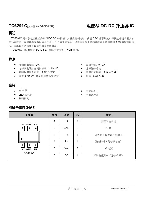
TC6291C (文件编号:S&CIC1159) 电流型DC-DC 升压器IC概述TC6291C 是一款电流模式升压型DC-DC 转换器。
其脉宽调制电路,内置0.2Ω功率场效应管使这个调节器具有高功率效率。
内部补偿网络也减少了多达6个的外部元件。
误差信号放大器的同相输入端连接到0.6V 精密基准电压,内部软启动功能可以减小瞬间突增电流。
TC6291C 可以封装为SOT23-6,在应用中节省了PCB 空间。
特点可调输出高达12V ;内部固定的脉宽调制频率:1.0MHZ 精准反馈参考电压:0.6V (±2%) 内置0.2Ω, 2A, 16V 的功率场效应管关断电流:0.1µA 过温保护功能可调过流保护:0.5A ~ 2.5A封装:SOT23-6应用充电器 LED 显示屏 数码相机 手持设备 便携式产品引脚示意图及说明TC6291C (文件编号:S&CIC1159) 电流型DC-DC 升压器IC功能框图21DCB0.3V0.6V短路比较器误差放大器UVLO关机电路软启动脉宽调制比较器振荡器斜率补偿OT P控制和驱动逻辑可调电流限制电流检测放大器Σ12345610KΩ - 100KΩ2.5A - 0.5A最大额定值参数 符号 测试条件最小值 典型值 最大值 单位 电源电压 Vcc 0 6 V LX 电压 Vlx 0 16 V EN 、FB 电压0 6 V 功耗 Pd SOT23-6@Ta=25℃455 m W 热阻 θJA SOT23-6+220 ℃/W 结温 Tj +150 ℃ 工作温度 Top -40 +85 ℃ 储存温度 Tst -65 +150 ℃ 管脚温度锡焊,10秒+260℃TC6291C(文件编号:S&CIC1159)电流型DC-DC升压器IC 典型工作特性(Vcc=3.3V,Vout=5V,Ta=25℃,除特殊说明外)效率VS输出电流电流限制VS外部电阻(Roc)工作频率VS输入电压工作频率VS温度参考电压VS输入电压参考电压VS输出电流TC6291C(文件编号:S&CIC1159)电流型DC-DC升压器IC 静态电流VS输入电压平均供电电流VS输入电压功能描述操作TC6291C是电流模式升压转换器。
稳压IC DC-DC 大全(带图)AMS117-3.3V 1A VIN<12VAMS 117-2.5V 1A VIN<12VAMS 117-1.8V 1A VIN<12VAMS 117-5V 1A VIN<12VAMS117-ADJ 1A VIN<12V(DC/DC) DC-DCTD1410 2A VIN<20V MP1580 2A VIN<25VMP1583 3A VIN<23V MPS1410/9141 2A VIN<15VMP1591 2A VIN<32V MP34063 1.5A VIN<40VACT4060 2A VIN<20V MP1482/MP2307 2A VIN<18VMP1484 3A VIN<23V TD6811 1.2A VIN<6VAP1513 2A VIN<18V7805 正5V稳压器(1A) 7805中文资料.pdf下载7806 正6V稳压器(1A)7808 正8V稳压器(1A)7809 正9V稳压议(1A)7809中文资料7812 正12V稳压器(1A) 7812中文资料7815 正15V稳压器(1A) 三端稳压器7815中文资料7818 正18V稳压器(1A)7824 正24V稳压器(1A)78L05 正5V稳压器(100ma)78L06 正6V稳压器(100ma)78L08 正8V稳压器(100ma)78L09 正9V稳压器(100ma)78L12 正12V稳压器(100ma)78L15 正15V稳压器(100ma)78L18 正18V稳压器(100ma)78L24 正24V稳压器(100ma)7905 负5V稳压器(1A)7906 负6V稳压器(1A)7908 负8V稳压器(1A)7909 负9V稳压器(1A)7912 负12V稳压器(1A)7915 负15V稳压器(1A)7918 负18V稳压器(1A)7924 负24V稳压器(1A)***************************************79L05 负5V稳压器(100ma)79L06 负6V稳压器(100ma)79L08 负8V稳压器(100ma)79L09 负9V稳压器(100ma)79L12 负12V稳压器(100ma)79L15 负15V稳压器(100ma)79L18 负18V稳压器(100ma)79L24 负24V稳压器(100ma)***************************************LM1575T-3.3 3.3V简易开关电源稳压器(1A)LM1575T-5.0 5V简易开关电源稳压器(1A)LM1575T-12 12V简易开关电源稳压器(1A)LM1575T-15 15V简易开关电源稳压器(1A)LM1575T-ADJ 简易开关电源稳压器(1A可调1.23 to 37)LM1575HVT-3.3 3.3V简易开关电源稳压器(1A)LM1575HVT-5.0 5V简易开关电源稳压器(1A)LM1575HVT-12 12V简易开关电源稳压器(1A)LM1575HVT-15 15V简易开关电源稳压器(1A)LM1575HVT-ADJ 简易开关电源稳压器(1A可调1.23 to 37)**************************************LM2575T-3.3 3.3V简易开关电源稳压器(1A)LM2575T-5.0 5V简易开关电源稳压器(1A)LM2575T-12 12V简易开关电源稳压器(1A)LM2575T-15 15V简易开关电源稳压器(1A)LM2575T-ADJ 简易开关电源稳压器(1A可调1.23 to 37)LM257HVT-3.3 3.3V简易开关电源稳压器(1A)LM2575HVT-5.0 5V简易开关电源稳压器(1A)LM2575HVT-12 12V简易开关电源稳压器(1A)LM2575HVT-15 15V简易开关电源稳压器(1A)LM2575HVT-ADJ 简易开关电源稳压器(1A可调1.23 to 37)**************************************LM2576T-3.3 3.3V简易开关电源稳压器(3A)LM2576T-5.0 5.0V简易开关电源稳压器(3A)LM2576T-12 12V简易开关电源稳压器(3A)LM2576T-15 15V简易开关电源稳压器(3A)LM2576T-ADJ 简易开关电源稳压器(3A可调1.23V to 37V)LM2576HVT-3.3 3.3V简易开关电源稳压器(3A)LM2576HVT-5.0 5.0V简易开关电源稳压器(3A)LM2576HVT-12 12V简易开关电源稳压器(3A)LM2576HVT-15 15V简易开关电源稳压器(3A)LM2576HVT-ADJ 简易开关电源稳压器(3A可调1.23V to 37V) **************************************LM2930T-5.0 5.0V低压差稳压器LM2930T-8.0 8.0V低压差稳压器LM2931AZ-5.0 5.0V低压差稳压器(TO-92)LM2931T-5.0 5.0V低压差稳压器LM2931CT 3V to 29V低压差稳压器(TO-220,5PIN)LM2940CT-5.0 5.0V低压差稳压器LM2940CT-8.0 8.0V低压差稳压器LM2940CT-9.0 9.0V低压差稳压器LM2940CT-10 10V低压差稳压器LM2940CT-12 12V低压差稳压器LM2940CT-15 15V低压差稳压器**************************************LM123K 5V稳压器(3A)LM323K 5V稳压器(3A)LM117K 1.2V to 37V三端正可调稳压器(1.5A)LM317LZ 1.2V to 37V三端正可调稳压器(0.1A)LM317T 1.2V to 37V三端正可调稳压器(1.5A)LM317K 1.2V to 37V三端正可调稳压器(1.5A)LM133K 三端可调-1.2V to -37V稳压器(3.0A)LM333K 三端可调-1.2V to -37V稳压器(3.0A)LM337K 三端可调-1.2V to -37V稳压器(1.5A)LM337T 三端可调-1.2V to -37V稳压器(1.5A)LM337LZ 三端可调-1.2V to -37V稳压器(0.1A)LM150K 三端可调1.2V to 32V稳压器(3A)LM350K 三端可调1.2V to 32V稳压器(3A)LM350T 三端可调1.2V to 32V稳压器(3A)LM138K 三端正可调1.2V to 32V稳压器(5A)LM338T 三端正可调1.2V to 32V稳压器(5A)LM338K 三端正可调1.2V to 32V稳压器(5A)LM336-2.5 2.5V精密基准电压源LM336-5.0 5.0V精密基准电压源LM385-1.2 1.2V精密基准电压源LM385-2.5 2.5V精密基准电压源LM399H 6.9999V精密基准电压源LM431ACZ 精密可调2.5V to 36V基准稳压源LM723 高精度可调2V to 37V稳压器LM105 高精度可调4.5V to 40V稳压器LM305 高精度可调4.5V to40V稳压器MC1403 2.5V基准电压源MC34063 DC-DC直流变换器mc34063中文资料pdf SG3524 脉宽调制开关电源控制器sg3524中文资料TL431 精密可调2.5V to 36V基准稳压源tl431a pdf 中文资料TL494 脉宽调制开关电源控制器tl494中文资料pdf下载TL497 频率调制开关电源控制器tl497/tl497A pdf datasheet TL7705 电池供电/欠压控制器。
300mA、500KHz高效率升压型DC-DC转换器描述是一款微型扁平封装、高效率、低压启动的升压型DC-DC转换芯片。
芯片内部包括误差放大器、振荡器、电流比较器、斜坡补偿、电流采样、逻辑驱动等模块。
峰值电流模式的PWM控制环路以及补偿网络的内部集成,使该芯片无需外围补偿元件即可在宽负载范围内提供稳定的输出电压。
SOT-23-6启动电压低于0.85V,适用于1-4节AA电,并且提供高达300mA的输出电流;500KHz的高频率允许采用纤巧的外围元器件如贴片电感和陶瓷电容,从而最大限度的减小了整体解决方案的占板面积;轻负载省电模式,仅消耗20μA的静态电流,延长了电池的使用寿命。
另外该芯片还具有远低于1μA的关断电流。
SOT-89-5主要特点* 0.85V的低电压启动* 单节AA电池100mA、双节AA电池300mA输出电流能力* 轻负载自动进入省电模式,仅需μA静态电流* 效率高达90%* +0.3V~+5V的输入工作电压范围* +2.5V~+6V的输出工作电压范围* 关断电流小于* 500KHz的固定开关频率* 过温保护* 4KV HBM ESD保护* 纤小型SOT-23-6和SOT-89-5封装应用* MP3播放机* 数码相机* 个人数字助理产品规格分类* LCD屏* 便携式仪器* 无线通讯装置产品封装形式SOT-23-6SOT-89-5共10页 第1页1uAHY3100HY3100HY3100 采用HY3100HY3100A内部框图极限参数 (T amb=25°C)参 数 参 数 范 围 单 位V DD工作端电压范围-0.3 ~ +6 V开关端电压范围-0.3 ~ +6 V使能端电压-0.3 ~ +6 V反馈端电压-0.3 ~ +6 V°C工作环境温度-40 ~ + 85贮存温度-65 ~ +125 °C电气参数 (除非特别注明,否则T amb =25°C,VI N=1.5V,V DD=3.3V,负载电流为0)参 数 符 号 测 试 条 件 最小值典型值 最大值 单位最小启动电压V ST I L=1mA --0.850.9V 最小输入电压V INMIN启动之后的VIN仅受输出功率限制-- 0.3 0.4 V工作电压范围V DD 2.5 --6 V反馈端电压V FB-- 1.23 V静态电流(轻载省电模式)I switch off FB=1.4V -- 20 30 μA(见下页)共10页 第2页(接上页)参 数 符 号 测 试 条 件最小值典型值 最大值 单位静态电流(关机状态模式)I st EN=0V -- 0.1 1 μA静态电流(PWM工作模式)I Q测试V DD端电流,无开关-- 300 360 μA进入省电模式的负载门限I load L= 4.7μH -- 7.5 -- mA输出电压线性调整率△V LINE 1V≤V IN≤3 V -- 2 10 mV/V输出电压负载调整率△V LOAD 1mA≤ I L ≤100mA --0.11mV/mA开关频率Fs -- 450 500 550 KHz最大占空比D MAX FB= 1.1V 90 95 %NMOS开关管导通电阻R ON V DD= 3.3V --0.40.5ΩNMOS开关管漏电流I leak V LX=5V --0.1ANMOS开关管限流值I LIMIT0.75 1.25 AEN输入高电平V H -- 1 VEN输入低电平V L -- -- 0.35 V热关断温度T j(sd)-- 150 C热关断迟滞温度T hyst C-- 20管脚排列图管脚描述管脚号管脚名称I/O 管脚说明1 1 ENI使能输入端。
1W isolated DC/DC converter in SIP package Wide input and regulated dual/single outputPatent Protection RoHSFEATURES●Ultra compact SIP package ●Wide input voltage range (2:1)●Operating temperature range:-40℃to +85℃●I/O Isolation test voltage:1.5K VDC ●Low ripple &noise●Short-circuit protection (self-recovery)●Remote On/Off ●EN62368approvedWRA_S-1WR2&WRB_S-1WR2series are isolated 1W DC-DC products with 2:1input voltage and conventional voltage output.The product has a relatively compact SIP-8plastic package,and features high efficiency,operating temperature of -40℃to +85℃,remote control,and continuous short-circuit protection.The smaller size and cost-effective design make the converter an ideal solution in communication,instruments,and industrial electronics applications.Selection GuideCertificationPart No.Input Voltage (VDC)OutputRipple &Noise (mVp-p)Typ./Max.Full Load Efficiency (%)Min./Typ.Capacitive Load ②(µF)Max.Nominal (Range)Max.①Voltage(VDC)Current (mA)Max./Min.CEWRA0505S-1WR25(4.5-9)11±5±100/±570/10071/731000WRA0512S-1WR2±12±42/±274/76470WRA0515S-1WR2±15±33/±273/75330WRB0503S-1WR2 3.3303/1569/711800WRB0505S-1WR25200/1070/722200WRB0512S-1WR21283/474/761000WRB0515S-1WR21567/373/75680WRB0524S-1WR22442/271/73470WRA1205S-1WR212(9-18)20±5±100/±5100/15076/781000WRA1212S-1WR2±12±42/±279/81470WRA1215S-1WR2±15±33/±276/78330WRB1203S-1WR2 3.3303/1573/752700WRB1205S-1WR25200/1075/772200WRB1209S-1WR29111/677/791800WRB1212S-1WR21283/477/791000WRB1215S-1WR21567/378/80680WRB1224S-1WR22442/274/76470WRA2405S-1WR224(18-36)40±5±100/±570/10077/791000WRA2409S-1WR2±9±56/±377/79680WRA2412S-1WR2±12±42/±277/79470WRA2415S-1WR2±15±33/±277/79330WRB2403S-1WR2 3.3303/1573/752700WRB2405S-1WR25200/1075/772200WRB2412S-1WR21283/476/781000WRB2415S-1WR21567/376/78680WRB2424S-1WR22442/275/77470WRA4805S-1WR248(36-75)80±5±100/±5100/15074/761000WRA4812S-1WR2±12±42/±276/78470WRA4815S-1WR2±15±33/±278/80330WRB4803S-1WR23.3303/1573/752700Input SpecificationsItemOperating Conditions Min.Typ.Max.Unit Input Current (full load/no-load)5VDC Input--281/40290/60mA12VDC Input --111/15114/3024VDC Input --55/657/10mA48VDC Input --27/428/6Reflected Ripple Current5VDC Input--30--12VDC Input --40--24VDC Input --55--48VDC Input --45--Surge Voltage (1sec.max.)5VDC Input-0.7--12VDC12VDC Input -0.7--2524VDC Input -0.7--5048VDC Input -0.7--100Starting Voltage5VDC Input---- 4.512VDC Input ----924VDC Input ----1848VDC Input----36Input Filter Filter capacitor Hot PlugUnavailableCtrl*Module onCtrl pin open (high resistance)Module offCtrl pin pulled high(current 5-10mA typ.into Ctrl.)Note:*For use of Ctrl,please refer to the “design reference”in this manual.Output SpecificationsItemOperating ConditionsMin.Typ.Max.UnitOutput Voltage Accuracy5%-100%load ,Input voltage range 3.3V/5V output --±2±5%others--±1±3No-load Output Voltage Accuracy Input voltage range--±1.5±5Linear Regulation Input voltage variation from low to high at full load--±0.2±0.5Load Regulation 5%-100%load--±0.4±0.75Transient Recovery Time 25%load step change --0.52ms Transient Response Deviation --±2.5±5%Temperature Coefficient Full load--±0.02±0.03%/℃Short Circuit ProtectionContinuous,self-recoveryNote:*The ”parallel cable”method is used for Ripple and Noise test,please refer to DC-DC Converter Application Notes for specific information.General SpecificationsItemOperating ConditionsMin.Typ.Max.UnitIsolationInput-output,with the test time of 1minute and the leak current lower than 1mA 1500----VDC Insulation Resistance Input-output,isolation voltage 500VDC 1000----M ΩIsolation Capacitance Input-output,100KHz/0.1V --120--pF Operating Temperature see Fig.1-40--+85℃Storage Temperature-55--+125℃Pin Soldering Resistance Temperature Soldering spot is1.5mm away from case for10seconds----+300℃Storage Humidity Non-condensing----95%RH Switching Frequency(PFM Mode)Full load,nominal input voltage--200--KHz MTBF MIL-HDBK-217F@25℃1000----K hoursMechanical SpecificationsCase Material Black flame-retardant and heat-resistant plasticDimension22.00×9.50×12.00mmWeight 4.5g(Typ.)Cooling Method Free air convectionElectromagnetic Compatibility(EMC)EMI CE CISPR32/EN55032CLASS B (see Fig.3-②for recommended circuit) RE CISPR32/EN55032CLASS B(see Fig.3-②for recommended circuit)EMS ESD IEC/EN61000-4-2Contact±4KV perf.Criteria B RS IEC/EN61000-4-310V/m perf.Criteria A EFT IEC/EN61000-4-4±2KV(see Fig.3-①for recommended circuit)perf.Criteria B Surge IEC/EN61000-4-5line to line±2KV(see Fig.3-①for recommended circuit)perf.Criteria B CS IEC/EN61000-4-63Vr.m.s perf.Criteria A Voltage dips,short interruptionsand voltage variations immunity IEC/EN61000-4-290%,70%perf.Criteria BTypical Characteristic CurvesFig1Design ReferenceAll DC-DC converters of this series are tested before delivery using the recommended circuit shown in Fig.2.Input and/or output ripple can be further reduced by appropriately increasing the input &output capacitor values Cin and Cout and/or by selecting capacitors with a low ESR (equivalent series resistance).Also make sure that the capacitance is not exceeding the specified max.capacitive load value of the product.Single1V inG N C d C in 1C in 2L in 2687Vo0VC S 3RD 1V cL c C o u tDual+Vo 0V Cout 687CoutLoutLout-VoCin1Vin21Lin3VcRIc D1Cd Cin2Vin5VDC&12VDC 24VDC&48VDC Cin1100µF/25V 10µF/100V Cin247µF/25V1µF/100VLin 4.7µH-12µH Cs10µF-22µF/50VCout Vo(3/±3/5/±5/9/±9V):100µF/16VVo(12/±12/15/±15V):100µF/25V Vo(24/±24V):100µF/50VLout 2.2μH-10μH Cd47nF/100V2.EMC compliance circuitLDM1②C0MOVFUSE①C1+VinGND+Vo-Vo (0V)DC/DCLOADC2CY CtrlCd D1R③CtrlVin1C3Parameter description:ModelVin:5VDC Vin:12VDC Vin:24VDC Vin:48VDC FUSE Slow blown fuses according to the actual input current selections of the clientsMOV --S14K25S14K35S14K60C01000µF/16V1000µF/25V 330µF/50V330µF/100V C1 4.7µF/50V4.7µF/100V LDM112µHC2 4.7µF/50V4.7µF/100VC3Refer to the Cout in Fig.2CY11nF/2KV D160V/1AR In accordance with the formula:300-0.1--CD C I V V R =Cd47nF/100VNotes:①For EMC tests we use Part ①in Fig.3for immunity and part ②for emissions test.Selecting based on needs.②V C is the voltage of the Ctrl end relative to the GND of the input grounding;V D is the positive-going conduction pressure drop of D1;I C is the current flows into the Ctrl end and its value is generally 5-10mA,see Fig.3-③for the peripheral circuit of Ctrl end;③If there is no recommended parameters,no external component is required.3.Ctrl endThe modules are of normal output when the Ctrl end is suspended or of high resistance;the modules turn off when connecting with high level (relative to the input grounding);notice that the current flows into the pin shall be 5-10mA,the modules will be permanently damaged if the current exceeds its max.value (20mA in general).The value of R can be derived as follows:300-0.1--C D C I V V R =For Detailed parameter,please refer to EMC solution-recommended circuit in this manual.4.Input currentWhen the electricity is provided by the unstable power supply,please make sure that the range of the output voltage fluctuation and the ripple voltage of the power supply do not exceed the indicators of the modules.Input current of power supply should afford the flash startup current of this kind of DC/DC module(see Fig.5).Generally:Vin=5V series Iave =445mAVin=12V series lave =205mA Vin=24V series lave =104mA Vin=48V series lave =53mAInput Voltage (V)Input Voltage scopeIaveFig.55.Output load requirementsWhen using,the minimum load of the module output should not be less than 5%of the nominal load.In order to meet the performance parameters of this datasheet,please connect a 5%dummy load in parallel at the output end,the dummy load is generally a resistor,please note that the resistor needs to be used in derating.6.For more information please find DC-DC converter application notes on Dimensions and Recommended LayoutNotes:1.For additional information on Product Packaging please refer to .Packaging number:58210004;2.Recommend to use module with more than5%load,if not,the ripple of the product may exceeds the specification,but does notaffect the reliability of the product;3.The recommended unbalance degree of the dual output module load is≤±5%;if the degree exceeds±5%,then the productperformance cannot be guaranteed to comply with all parameters in the datasheet.Please contact our technicians directly for specific information;4.The maximum capacitive load offered were tested at input voltage range and full load;5.Unless otherwise specified,parameters in this datasheet were measured under the conditions of Ta=25℃,humidity<75%RH with nominalinput voltage and rated output load;6.All index testing methods in this datasheet are based on company corporate standards;7.We can provide product customization service,please contact our technicians directly for specific information;8.Specifications are subject to change without prior notice.Mornsun Guangzhou Science&Technology Co.,Ltd.Address:No.5,Kehui St.1,Kehui Development Center,Science Ave.,Guangzhou Science City,Huangpu District,Guangzhou,P.R.China Tel:86-20-38601850Fax:86-20-38601272E-mail:***************。