电子设计自动化(EDA)
- 格式:ppt
- 大小:1.09 MB
- 文档页数:18
第一章EDA概述1.1EDA技术的涵义一、EDA技术的涵义EDA(Electronic Design Automation)即电子设计自动化是指利用计算机完成电子系统的设计。
二、 EDA技术的分类EDA技术分:广义的EDA技术和狭义的EDA技术广义的EDA技术是指以计算机和微电子技术为先导,汇集了计算机图形学、数据库管理、图论和拓扑逻辑、编译原理、微电子工艺与结构学和计算数学等多种计算机应用学科最新成果的先进技术。
狭义的EDA技术是指以大规模可编程逻辑器件为载体,以硬件描述语言HDL为系统逻辑的主要表达方式,借助功能强大的计算机,在EDA 工具软件平台上,对用HDL描述完成的设计文件,自动完成用软件方式设计的电子系统到硬件系统的逻辑编译、逻辑简化、逻辑分割、逻辑综合及优化、逻辑布局布线、逻辑仿真,直至对特定目标芯片的适配编译、逻辑映射、编程下载等工作,最终形成集成电子系统或专用集成芯片ASIC(Application Specific Integrated Circuits)的一门新技术。
本书中提到的EDA技术指的是狭义的EDA技术。
1.2EDA技术的发展历史EDA技术的发展,大致经历了三个发展阶段:1.计算机辅助设计CAD 2.计算机辅助工程设计CAE 3.电子设计自动化EDA1.3 EDA技术的基本特征EDA技术的基本特征主要包括:1.EDA技术采用自顶向下的设计方法2.EDA技术的设计语言是硬件描述语言3.EDA技术具有逻辑综合和优化的功能4.EDA技术采用开放性和标准化的软件框架1.4 EDA的主要内容EDA技术主要这几方面的内容: 1.可编程逻辑器件2.硬件描述语言3.软件开发工具1.可编程逻辑器件可编程逻辑器件是一种由用户编程以实现某种逻辑功能的新型件。
可编程逻辑器件也称为可编程ASIC,它是EDA技术的物质基础。
2.硬件描述语言HDL语言是EDA技术的重要组成部分,它是一种用于描述硬件电子系统的计算机语言,它用软件编程的方式来描述电子系统的逻辑功能、电路结构和连接形式。
电子设计自动化(EDA)绪论引言电子设计自动化(Electronic Design Automation,EDA)是利用计算机辅助设计(Computer-ded Design,CAD)技术来辅助电子系统的设计和开发的一门学科。
随着电子技术的发展和电子产品的普及,EDA在现代电子工程中扮演着重要的角色。
本文将介绍电子设计自动化的发展历程、应用领域以及未来趋势。
发展历程EDA的起源可以追溯到20世纪50年代末的数学计算和电子计算机出现之前。
当时,电子设计工程师需要手工布线、调整参数并进行实验验证。
正是因为这种繁琐的工作方式,才催生了EDA这一概念的提出和应用的需求。
随着计算机技术的发展,EDA得到了广泛的应用,大大提高了电子设计的效率和准确性。
应用领域EDA在电子工程的各个领域都有着广泛的应用。
以下是一些主要的应用领域:1.集成电路设计:EDA在集成电路设计中发挥着核心作用。
它可以实现逻辑设计、物理设计、电路模拟、验证等功能。
EDA工具可以帮助工程师完成复杂的电路设计、优化电路性能并减少设计周期。
2.PCB设计:EDA在PCB(Printed CircuitBoard)设计中也有重要应用。
通过使用EDA工具,工程师可以根据电路原理图自动生成PCB布局,协助进行电气和机械检查,提高PCB设计的效率和可靠性。
3.系统级设计:EDA在系统级设计中起到了重要的支持作用。
它可以协助工程师进行系统级建模、分析和优化,保证系统的正确性和可靠性。
4.验证和仿真:EDA工具可以进行电路的验证和仿真,帮助工程师在硬件设计之前发现可能存在的错误,提高设计的质量和稳定性。
5.封装和测试:EDA在封装设计和测试过程中提供了许多有用的工具和方法。
这些工具可以帮助工程师进行封装选择、封装布局以及封装测试,提高封装的成功率和可用性。
未来趋势随着信息技术的不断发展,EDA也在不断演进和改进。
以下是一些EDA未来的发展趋势:1.机器学习的应用:随着机器学习技术的迅速发展,EDA也可以应用机器学习来优化设计过程和结果。
---------------------------------------------------------------最新资料推荐------------------------------------------------------eda简介(eda简介)eda 简介(eda 简介) EDA in the communications industry (Telecommunication) another explanation is the enterprise data architecture, EDA gives a general view of an enterprise data architecture, and in accordance with the characteristics of telecom enterprises, the framework and hierarchy. EDA is an electronic design automation (Electronic Design Automation): from the computer aided design in the middle of 1960s (CAD), computer aided manufacturing (CAM), computer aided test (CAT) and Computer Aided Engineering (CAE) and the concept of development. Catalog First, what is EDA? Two, design methods Three 、 EDA tool software classification Four, EDA tool software vendors tycoon three Five, compounds Six. Exploratory data analysis Seven. Distribution estimation algorithm 1. What is EDA? Two, design methods Three 、 EDA tool software classification Four, EDA tool software vendors tycoon three Five, compounds Six. Exploratory data analysis Seven, distribution estimation algorithm Edit this paragraph 1. What is EDA? In 1990s, the international advanced electronic and computer technology in the world, has been exploring new methods of electronic circuit design actively,1 / 23and made a thorough change in design methods, tools etc, with great success. In the field of electronic technology design, the application of programmable logic devices (such as CPLD, FPGA) has been widely popularized. These devices bring great flexibility to the design of digital systems. These devices can be programmed by software to reconstruct their hardware structure and working mode, so that the hardware design can be as convenient and fast as the software design. All these greatly changed the traditional digital system design method, design process and design concept, and promoted the rapid development of EDA technology. EDA technology is a computer as a tool for designers in the EDA software platform, using hardware description language VHDL to complete the design documents, and then the computer automatically complete logic compilation, simplification, segmentation, synthesis, optimization, layout, simulation, adaptive translation, logical mapping and programming work until the chip for the specific target the. The emergence of EDA technology greatly improves the efficiency and operability of circuit design, and reduces the labor intensity of designers. Using EDA tools, the electronics designer can start the electronic system design from concept, algorithm and protocol, a lot of work can be done through the---------------------------------------------------------------最新资料推荐------------------------------------------------------ computer and electronic products can be from circuit design and performance analysis to design the whole process of IC territory or PCB layout of the computer automatically complete the processing. Now, the concept or category of EDA is very wide. Including mechanical, electronic, communications, aerospace, chemical, mineral, biological, medical, military and other fields, there are EDA applications. At present, EDA technology has been widely used in major companies, enterprises and institutions and scientific research and teaching departments. For example, in the aircraft manufacturing process, from design, performance testing and characteristic analysis until the flight simulation, may involve EDA technology. The concept of EDA EDA technology refers to the computer as the work platform, the latest achievements of the integration application of electronic technology, computer technology, information processing and intelligent technology, the automatic design of electronic products. Using EDA tools, the electronics designer can start the electronic system design from concept, algorithm and protocol, a lot of work can be done through the computer and electronic products can be from circuit design and performance analysis to design the whole process of IC3 / 23territory or PCB layout of the computer automatically complete the processing. Now, the concept or category of EDA is very wide. Including mechanical, electronic, communications, aerospace, chemical, mineral, biological, medical, military and other fields, there are EDA applications. At present, EDA technology has been widely used in major companies, enterprises and institutions and scientific research and teaching departments. For example, in the aircraft manufacturing process, from design, performance testing and characteristic analysis until the flight simulation, may involve EDA technology. This paper refers to the EDA technology, mainly for electronic circuit design, PCB design and IC design. EDA design can be divided into system level, circuit level and physical implementation level. Edit paragraph two, design method (1) front end design (system modeling, RTL level description), back end design (FPGAASIC) system modeling (2) IP multiplexing (3) front-end design (4) system description: establish the mathematical model of the system. (5) function description: describe the behavior of the system or the data flow diagram among the sub modules. (6) logic design: the system function is structured, usually with text, schematics, logic diagrams, Boolean expressions to represent the design results. (7)---------------------------------------------------------------最新资料推荐------------------------------------------------------ simulation: including function simulation and timing simulation, mainly verify the correctness and timing characteristics of the system function. Edit this paragraph three, EDA tool software classification EDA tool software can be roughly divided into three categories: chip design assistance software, programmable chip aided design software, system design auxiliary software and so on. Currently entering the country and has a wide influence in the EDA software system design software and programmable chip design software: Protel, Altium Designer, PSPICE, multiSIM10 (the latest version of the original EWB, OrCAD, PCAD), LSIIogic, MicroSim, ISE, Modelsim, Matlab and so on. These tools are strong function, generally can be used in several aspects such as many software can realize the circuit design and simulation, PCB automatic layout and also can output a variety of file with third party software interface. According to the main function or the main application situation, divided into circuit design and simulation tools, PCB design software, IC design software, PLD design tools and other EDA software, a brief introduction. 3.1 electronic circuit design and simulation tools, we may have used the test board or something else to make some electronic5 / 23system to practice. But sometimes, we find that there are a lot of problems to be done, not previously thought, so that waste our time and supplies. It also increases the product development cycle and extends the product listing time, so that the product loses the market competitive advantage. Is there a way to know the result without using the electric iron test board? The conclusion is that this is the circuit design and simulation technology. When it comes to electronic circuit design and simulation tools, this technology can not be mentioned in the United States, can not help but mention their aircraft design why high efficiency. Our previous design of a medium-sized aircraft, from the draft to the detailed design to the wind tunnel test, and finally to the map to the actual production, the entire cycle is about 10 years. And the United States is 1 years old. Why is there such a big gap? Because the United States is most used in the design of virtual simulation technology, the wind tunnel experiment parameters accumulated over the years into the computer, and then through the computer programming written in a virtual environment of software, and enable it to experience parameters automatically apply the relevant formula and call after long-term accumulated input computer. In this way, as long as the aircraft shape meter data---------------------------------------------------------------最新资料推荐------------------------------------------------------in the virtual wind tunnel test software, where unreasonable have changes there, until the best effect, efficiency is high, as long as the final test several times for shortage in the actual environment can be established, from their Boeing 747 to F16 is this method uses the. The aerodynamic data are provided by senior experts, and the software developer is IBM. The engineer of the aerocraft only needs to use the simulation software to do a variety of simulation debugging work on the computer platform. Similarly, many of their other things are using a similar approach, from big to small, from complexity to simplicity, and even to design furniture and composition, but the specific content of the software is different. In fact, they invented the first generation of computers for this purpose (originally for efficient design of artillery and related shells and other large amount of design). Electronic circuit design and simulation tools include SPICE/PSPICE; multiSIM7; Matlab; SystemView; mmicad LiveWire、爱迪生、蒂娜亲明亮的火花等。

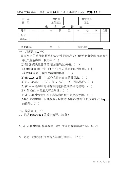
三、改错;找到5处错误并改正(10分)LIBRARY IEEE ;USE IEEE.STD_LOGIC_1164.ALL ;ENTITY CNT4 ISPORT ( CLK :IN STD_LOGIC ;Q :OUT STD_LOGIC_VECTOR(3 DOWNTO 0))END ;ARCHITECTURE bhv OF CNT ISSIGNAL Q1 : STD_LOGIC_VECTOR(3 DOWNTO 0);BEGINPROCESS (CLK)BEGINIF CLK'EVENT AND CLK THENQ1 〈= Q1 + 1 ;END PROCESS ;Q 〈= Q1 ;END bhv;四、设计,要求写出完整的vhdl代码。
(65分)1、16位硬件加法器,要求有进位输入和进位输出。
(15分)2、七段数码管译码显示电路设计(数码管共阳极接法)(12分)要求输入BCD码,输出驱动数码管显示0到93、十进制加法计数器,要求有复位功能。
(13分)4、上升沿触发的D触发器,要求用三种方式描述,实体可只写一个。
(15分)B : IN STD_LOGIC_VECTOR(15 DOWNTO 0) ;S : OUT STD_LOGIC_VECTOR(15 DOWNTO 0) ;COUT : OUT STD_LOGIC );END ADDER4B ;ARCHITECTURE behav OF ADDER16 ISSIGNAL SINT : STD_LOGIC_VECTOR(16 DOWNTO 0);SIGNAL AA,BB : STD_LOGIC_VECTOR(16 DOWNTO 0) ; BEGINAA〈='0'&A ;BB<=’0'&B ;SINT <= AA + BB + CIN ;S <= SINT(15 DOWNTO 0);COUT <= SINT(16);END behav ;实体正确7分,能完成加法5分,进位正确3分2、七段数码管译码显示电路设计(数码管共阳极接法)(12分)要求输入BCD码,输出驱动数码管显示0到9LIBRARY IEEE ;USE IEEE.STD_LOGIC_1164。

电子设计自动化(EDA)实验引言电子设计自动化(EDA)是一种利用计算机技术来辅助电子系统设计的工具和方法。
传统的电子设计过程通常需要进行大量的手工操作,但由于电子系统的复杂性不断增加,现代电子设计已经无法满足快速、高效、准确开发产品的需求。
因此,EDA成为了现代电子设计的关键技术。
本实验将介绍EDA的基本概念和相关工具,以帮助大家更好地理解和应用EDA技术。
1. EDA的定义EDA,即Electronic Design Automation,是指利用计算机和相关工具来辅助进行电子系统设计的一种技术。
它采用了计算机辅助设计(CAD)的概念和方法,结合了电路设计、逻辑设计、物理设计等多种技术,可大大提高电子系统设计的效率和可靠性。
EDA技术已经广泛应用于各个层次的电子系统设计中,包括电路设计、芯片设计、电路板设计等。
2. EDA的基本流程EDA的基本流程包括以下几个主要步骤:2.1 电路设计电路设计是EDA的首要步骤之一。
在电路设计阶段,需要通过选择合适的元器件和器件参数来构建电路图,并进行电路仿真和性能评估。
常用的电路设计工具包括Altium Designer、Cadence 等。
2.2 逻辑设计逻辑设计是EDA的核心步骤之一。
在逻辑设计阶段,需要将电路图转化为逻辑电路图,并进行逻辑仿真、逻辑综合等操作,以验证电路功能和性能的正确性。
常用的逻辑设计工具包括Verilog、VHDL等。
2.3 物理设计物理设计是EDA的重要步骤之一。
在物理设计阶段,需要进行芯片布局、布线规划、时钟树设计等操作,以实现电路的物理布局和布线,最终生成物理设计数据。
常用的物理设计工具包括Cadence、Synopsys等。
2.4 验证与验证验证与验证是EDA的关键步骤之一。
在验证与验证阶段,需要进行电路功能验证、时序验证、功耗验证等操作,以保证电子系统设计的正确性和可靠性。
常用的验证与验证工具包括Mentor、Cadence等。
《电子设计自动化(EDA)》课程标准课程名称:电子设计自动化(EDA)课程编码:0509069 学分:3总学时:54(30+24)适用专业:机电一体化专业一、前言1.课程性质《电子设计自动化(EDA)》课程是机电一体化专业必修的专业核心课程,是一门理实一体课程。
本门课程在第四学期开设,为专业核心课程,其前导课程是计算机应用基础,电路基础,电子技术基础。
为后续的“单片机技术与应用”等课程的综合设计打下了理论和实践的基础。
2.基本理念本课程是一门实践性非常强的课程。
要求学生注重实践,在掌握Protel 99 SE软件的基本操作后,重点加强PCB工程训练。
采用多媒体教学,实例分析教学。
3.设计思路(1)、以机电产品开发技术员以及开发助理员岗位完成机电产品硬件开发工作任务所需的能力要求作为课程内容选取的主要依据。
根据电子行业经济发展的需要,聘请企业技术人员对机电一体化专业领域的职业岗位进行工作任务分析,根据完成机电产品硬件开发典型工作任务所需的知识、能力和素质要求进行教学内容的选取。
(2)、结合国家职业标准确定了课程标准在课程主讲老师和企业专家共同参与下,根据行业对职业能力的要求,结合“计算机辅助设计绘图员(电子)(简称电子CAD绘图员)”国家职业标准,明确本课程教学内容及对各内容的掌握要求。
然后,根据典型工作任务的特点,将各教学内容进行知识的解构。
按照职业成长规律与认知学习规律,以项目的形式,将本课程分解为电源电路、信号源电路、智能温度计等六个电路由易至难、由简单到复杂的学习子领域,将之前解构的各知识点重构到相应的学习子领域中,真正实现“用什么,学什么”。
以项目为载体,设计完成子领域教学目标的学习情境,在学习情境中明确学习目标、学习内容、建议教学方法、教学材料、使用工具、学生知识能力的储备、教师要求、考核与评价。
(3)、基于行动导向原则进行教学模式设计采用工作过程系统化的课程改革方法,用三个学习情境贯穿教学组织,每一个学习情境都是一个完整的工作过程,无论是简单的还是复杂的电路,都经历了原理图设计——PCB设计——PCB制作等几个主要工作环节,与企业的PCB设计员实际所做的项目或工作完全一致,充分体现职业性。
电子工程设计的EDA技术详解电子工程设计是一门复杂的学科,需要高超的技术和技能才能成功完成。
为了简化工程设计,EDA技术应运而生。
EDA 技术是指电子设计自动化技术,是通过计算机软件和硬件工具辅助电子工程师完成电路设计、电路仿真、布局及版图设计和自动化测试等流程的一组技术。
这些技术已经成为全球电子工程设计的标准,本文将详尽介绍EDA技术。
一、EDA的历史发展EDA技术是在20世纪60年代末、70年代初出现的,随着计算机技术的发展而逐渐被广泛应用。
在当时,使用电路仿真工具和还原与印刷电路板设计等自动化技术的设计过程仍然需要耗费大量时间,但这项技术的出现使设计人员更快地获得模拟电路的准确性,设计效率也显著提高了。
在EDA的诞生初期,主要限制因素是缺乏高速计算机和处理器等硬件设备,当时的系统也缺乏必要的软件功能和设计方法,无法对大型电路进行完整的模拟和分析。
而如今,EDA技术已经迅速发展,已经基本成为电子工程领域的核心技术。
二、EDA技术的应用机制EDA技术利用计算机技术,以及从自动化设计到真实物理系统测试的各种工具来辅助电路设计全过程。
其完整应用包括了以下浅显组成机制:1、原语、模型库和输入通过系统的数据终端和透过特殊的软件来访问EDM模型库,工程师可以立刻从模型库中获取需要相应的电子元件模型、原语等。
2、应用的添加及网表生成EDA的利用者可以按照模型库添加自行的应用,随后通过软件对网表的作用,来管理整个电路。
同时,应用程序还能帮助电路设计者将电路转换为网络表,以更方便地进行后续的操作。
3、顶层设计在确定了电路元器件和电路板的所有附加元素的基础上,电路设计师就开始考虑如何将电路拼接在一起,并以最有效和可支持的方式实现电路的最终设计目标。
4、布局设计布局设计涉及到代替板上元器件的几何图形,包括元器件间的物理距离等。
电路板的布局设计受到很多因素的限制,例如电路板尺寸,供电要求和热排除等。
5、仿真通过计算机,EDA技术能够仿真检测电路功能和设计的可行性,并对电路进行性能测试。
(OA自动化)电子设计自动化(eda)实验指导书电子设计自动化(EDA)实验指导书前言近些年来,电子设计自动化(EDA)技术发展迅速。
一方面,各种大容量、高性能、低功耗的可编程逻辑器件不断推出,使得专用集成电路(ASIC)的生产商感受到空前的竞争压力。
另一方面,出现了许多EDA设计辅助工具,这些工具大大提高了新型集成电路的设计效率,使更低成本、更短周期的复杂数字系统开发成为可能。
于是一场ASIC与FPGA/CPLD之争在所难免。
然而PLD器件具有先天的竞争优势,那就是可以反复编程,在线调试。
EDA技术正是这场较量的推动引擎之一。
一般来说,EDA技术就是以计算机为平台,以EDA软件工具为开发环境,以HDL为设计语言,以可编程器件为载体,以ASIC、SOC芯片为目标器件,以电子系统设计为应用方向的电子产品自动化设计过程。
设计者只需编写硬件描述语言代码,然后选择目标器件,在集成开发环境里进行编译,仿真,综合,最后在线下载调试。
整个过程,大部分工作由EDA软件完成。
全球许多著名的可编程器件提供商都推出了自己的集成开发工具软件,如Altera公司的MAX+PLUSⅡ、QuartusⅡ软件;Xilinx公司的Foundation、ISE软件,Lattice公司的ispExpert软件,Actel 公司的Libero软件等。
这些软件的推出,极大地促进了集算法设计、芯片编程、电路板设计于一体的EDA技术的发展。
另外,在以SOC 芯片为目标器件的电子系统设计要求下,可编程器件的内部开始集成高速的处理器硬核、处理器软核、DSP模块、大量的存储资源、高速的串行收发模块、系统时钟管理器、多标准的I/O接口模块,亦使得设计者更加得心应手,新一轮的数字革命由此引发。
EDA技术是一门实践性很强的学科,要培养出具有竞争力的一流IC设计人才,动手能力是关键。
只有通过理论学习,加上现场实验,在使用软件编程加硬件调试的过程中真正获得锻炼,增长技能。
电子设计自动化1. 简介电子设计自动化(Electronic Design Automation,简称EDA)是一种利用计算机软件来辅助电子设计过程的技术。
它集成了多种工具和方法,用于设计、模拟、验证和制造电子系统。
EDA的应用范围广泛,包括集成电路、系统级芯片、电路板设计和封装等。
2. EDA的历史EDA技术的起源可以追溯到20世纪50年代,当时的电子设计主要是通过手工绘图和计算器来完成。
随着电子技术的迅速发展,电路复杂度不断增加,人工设计和验证的效率显著下降。
1960年代末,EDA开始出现,并逐渐成为电子设计的主要工具。
3. EDA的组成EDA系统通常由多个模块组成,包括以下主要模块:3.1 电路设计工具电路设计工具是EDA中最基础、最重要的模块之一。
它提供了创建、编辑和验证电路的功能,可以绘制电路图,并进行模拟分析和优化。
常见的电路设计工具包括Cadence、Mentor Graphics、Synopsys等。
3.2 电路仿真工具电路仿真工具是用于验证电路设计的重要模块。
它可以对电路进行数值仿真和时序仿真,以检测设计中的错误和故障。
常见的仿真工具有SPICE、HSPICE、PSpice等。
3.3 物理设计工具物理设计工具用于将电路设计转化为实际的物理布局。
它可以进行芯片的布局、布线和时序优化,以满足电路设计的性能要求。
常见的物理设计工具有Calibre、ICC、Encounter等。
3.4 设计验证工具设计验证工具用于对电路设计的正确性进行验证和测试。
它可以对电路进行功能仿真和时序验证,以确保设计的准确性和稳定性。
常见的验证工具有FormalPro、VCS、ModelSim等。
3.5 设备制造工具设备制造工具是用于电路生产和制造的模块。
它可以进行版图优化、掩膜生成和工艺仿真,以满足芯片制造的需要。
常见的设备制造工具有Calibre、Hermes、Tanner等。
4. EDA的优势EDA技术在电子设计过程中具有如下优势:•提高设计效率:EDA工具可以自动化设计流程,减少人工操作,提高设计效率和精度。
电子设计自动化(EDA)概述电子设计自动化(Electronic Design Automation,简称EDA)是一种利用计算机软件工具来设计和验证电子器件和系统的方法。
由于现代电子设备的复杂性和功能要求不断增加,传统的手工设计方法已经无法满足设计师们的需求。
EDA技术的发展使得电子设备的设计和验证过程更加快速、准确和可靠。
EDA的主要应用EDA技术主要应用于以下几个方面:1. 电路设计电路设计是EDA技术最早应用的领域之一。
通过EDA软件工具,设计师可以利用图形界面进行电路原理图的绘制和元件的布局。
EDA软件还可以帮助设计师进行性能分析、信号完整性分析和功耗优化等工作。
EDA技术的应用使得电路设计过程更加高效和可靠。
2. 片上系统设计片上系统(System-on-Chip,简称SoC)是现代电子设备中常见的组件,它集成了大量的电子元器件和功能模块。
EDA软件工具可以帮助设计师进行SoC的系统级设计、仿真和验证。
通过EDA技术,设计师可以在更短的时间内完成SoC 设计,提高生产效率和产品质量。
3. FPGA设计可编程逻辑门阵列(Field Programmable Gate Array,简称FPGA)是一种灵活可编程的集成电路。
EDA技术在FPGA设计中扮演着重要的角色。
设计师可以利用EDA软件工具进行FPGA的电路设计、布局和验证。
EDA技术的应用使得FPGA设计更加灵活、高效和可靠。
4. PCB设计印刷电路板(Printed Circuit Board,简称PCB)是电子设备中的重要组成部分。
EDA技术在PCB设计中发挥着关键的作用。
设计师可以通过EDA软件工具进行PCB的布线、信号完整性分析和电气规则检查等工作。
EDA技术的应用使得PCB设计过程更加高效和可靠。
EDA的工作流程EDA技术的工作流程主要包括以下几个步骤:1.需求分析和规格说明:在设计开始之前,设计师需要进行需求分析和规格说明,明确设计目标和功能要求。
《电子设计自动化(EDA)》课程标准课程名称:《电子设计自动化(EDA)》适用专业:中等职业学校《电子技术应用》专业1.前言1.1课程性质本课程是中等职业学校电子技术应用专业的一门专业任选课程。
其功能是使学生掌握电子设计自动化方面的基本知识和基本技能,具备绘制电路原理图、设计印制电路板、仿真电路图等基本职业能力,为就业作前期准备。
1.2设计思路本课程总体设计思路是以电子技术应用专业相关工作任务和职业能力分析为依据确定课程目标,设计课程内容,以工作任务为线索构建任务引领型课程。
本课程主要以电路原理图绘制、印制电路板设计及电路仿真三大模块为线索进行设计。
为了充分体现任务引领、实践导向的课程思想,将课程的教学内容设计成若干个工作任务,以工作任务为中心引出相关专业知识,展开教学活动。
充分运用现代职教理念与技术,将教学和岗位的需求结合起来,将工艺规范与行业规范融入到课程中,培养学生自主学习的能力,团队协作的能力和与人沟通的能力。
使学生树立规范意识,质量意识,为以后的就业和职业发展奠定基础。
建议课时100学时。
2.课程目标过本课程的学习,能了解Protel DXP 2004软件的特点及运行环境,掌握应用Protel DXP 2004软件进行原理图绘制、电路仿真、印制电路板设计等操作,初步具备独立运用电子线路CAD软件进行简单电路设计的能力,同时提高学生分析问题的能力,合作沟通的能力,养成诚实守信的品质。
职业能力目标:●能使用Protel DXP 2004绘制电路原理图●能使用Protel DXP 2004设计印制电路板图●能使用Protel DXP 2004对电路进行仿真●能创建元件电气图形符号及封装图●具备严谨的专业思想和良好的职业道德3.课程内容与要求4.实施建议4.1教材编选1.教材选用中国水利水电出版社的《电子线路设计--Protel DXP 2004 SP2》,顾滨主编。
2.根据课程目标的要求,适当选用补充教材。