8730精密线材测试机中文使用手册 (2)
- 格式:pdf
- 大小:2.29 MB
- 文档页数:54
目录一、GeoPluse浅地层剖面仪操作规程 (1)1、仪器简介 (1)1)功能简介 (1)2)系统配置 (1)2、GeoPluse浅地层剖面仪系统配置连接 (1)1)换能器安装 (1)2)5430A收发机与5210A接收机连接 (2)3)接通电源 (4)3、5210A与5430A收发机功能键简介 (4)1)5430A收发机功能键简介 (5)2)5210A接收机功能键简介 (5)4、数据采集后处理 (7)二、Knudsen 320Ms双频测深仪操作规程 (14)1、仪器简介 (14)1)工作原理 (14)2)功能简介 (14)2、系统配置连接 (15)1)换能器连接 (15)2)Knudsen 320Ms主机与电脑的连接 (15)3)接通电源 (16)3、Knudsen 320Ms菜单结构 (16)4、数据采集后处理 (21)三、TideMaster型潮位仪操作规程 (29)1、仪器硬件设置 (29)1)主要设备仪器 (29)2)操作及安装使用 (31)2、临时验潮站站址选择原则 (31)3、仪器的软件设置 (31)四、GPS操作规程 (41)1、工作原理 (41)2、基准站操作 (41)1)仪器架设 (41)2)用手簿启动基准站 (44)3、Trimble SPS461 GPS罗经设置及使用说明 (46)1)网络连接方法设置461 (46)2)SPS461 信标机定位定向仪液晶屏设置说明 (51)五、海底管线铺设导航、定位技术 (64)1、GPS定位原理 (64)2、海洋定位技术 (65)1)差分GPS技术 (65)2)信标差分技术 (65)3、GPS 控制网及基准站的设立解算 (66)1)基准站的选定和设立 (66)2)GPS控制网的布设、施测和解算 (67)3)测区的坐标七参数的解算 (68)4)利用转化参数转换坐标 (69)4、海底管道施工导航定位技术 (69)1)海底管线临时定位桩施工 (69)2)铺管船法海底管线铺设导航定位 (71)六、海底管线预、后调查方案 (75)1、概述 (75)1)项目概述 (75)2)海底管线状态简介 (75)2、使用检测仪器进行海底管线铺设后调查内容 (76)1)海底管线外观检查 (76)2)经处理后的完工调查 (77)3、后调查作业设备及选用原则 (77)1)测深设备 (77)2)旁侧声纳 (78)3)浅地层剖面仪 (78)4、调查作业施工 (79)1)作业准备 (79)2)计划线布设 (79)3)作业方法和步骤 (80)4)作业注意事项 (82)5、数据采集、记录以及报告 (83)1)数据采集 (83)2)数据处理 (84)6、组织机构与职责 (85)一、GeoPluse浅地层剖面仪操作规程1、仪器简介1)功能简介使用GeoPluse浅地层剖面,得到几十米深的纵断面工程地质图,探明海底泥层的构成、岩性、断层位置以及有无埋设其他管道等,然后将所取得的几条走向资料进行对比,以确定最优的路由。
文件名称版本(精密线材)电测机操作指导书A/1生效日期2020年4月22日页码Page 3 of 61.目的依据此规范进行合理、科学的检验,保证产品符合客户品质要求。
2.适用范围本公司所有数据线,充电线类产品均适用之。
3.主要职责测试员: 负责对全厂线材类产品测试及判定,并记录。
组长:负责对测试员测试的监督及确认。
Q E: 负责对检验治具、设备的调校。
品质主管:负责对本规范的制定、及修正。
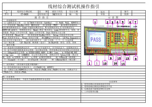
4.定义:(无)5.工作程序5.1测试工具:测试治具5.2主要测试参数标准:a. 电源电压:220V±10% 50Hz,通常仪器测试规格:绝缘5MΩ,电压300VDC.b. 依《检验规范》c. 产品《工程图》5.3操作步骤:a.开机时,喇叭响一声,测试机进入待机状态,LCD显示:【 HR--3800 V3.1 】【 Continuity Tester 】;此时机器进行自我测试,如果测试正常,则LCD显示⑹【 Avaliable Cards:1 】【 **Self Test OK ** 】;若自我测试时发现错误,LCD显示:【 Avaliable Cards:0 】【 Self Test Error 】;此时需通知相关人员进行或厂商调试。
1 2b.开机后,点击ENTER进入设定界面,进入①:测试模式设定,短断路设定,导通电阻设定,被动元文件名称版本(精密线材)电测机操作指导书A/1生效日期2020年4月22日页 码Page 4 of 6件设定,高压条件设定,测试项目设定等.另外点击面板上的PARA 键也可进入②测试模式设定,此时可对 自动测试 或 测试次数 进行设定.c.在开机后界面点击FILE,可进入③④:如果样品名称或路径不符合你的试品,但你的试品在选项中,则点击上下左右方向键选中,再按面板上的ENTER 确认即可.如下图:点击面板上的FILE 键名时,进入,样品程序选定,按右边面板上黑色键即可保存.例如,你要测试的试品为1256C,如果当前默认选项为此样品,则直接在面板上点击ENTER 确认即可,如果没有,则退出,点击LEARN 进入,然后将样品插入连接器端口,点击面板上的TEST 测试键或输入新样品名,点击ENTER 确认即可,此时将试品插入,然后进行测试:点对点,数据储存(确认10PIN 对 NET5,或8PIN 对NET4).即可测试了.如果你的试品在样品路径或程序中没有,则在开机界面点击LEARN,然后插好试品,点击TEST 测试,再填好名称或编码按ENTER 确认保存即可.在填入字母或数字时,可通过方向键移位(或通过速度快慢转换字母或数字输入).如果测试夹具或连接端口有变动,则如⑤,点击开机界面,FUNC 键名,则出现输入点位寻找的菜单选项.试品插好后,点击ENTER 即可寻找.单词:cable stat file para,open,short,shift,learn,print,enter,sys,exit,enter 等单词.依次分别为:线材,开始,文件夹,参数,开路,短路,转换,学习,打印,进入或确认,退出,进入5634文件名称版本(精密线材)电测机操作指导书A/1生效日期2020年4月22日页 码Page 5 of 6点击SYS 为系统状态,如图⑨.c.把所要测试的治具插好,拿一条标准产品插入治具内,按"5"键两下,机器进行读取相应的数据,并进入设置状态,看LCD 显示的项目按上下左右箭头键进行设置,并参照相应的作业指导书。
1 OF 4总页数
核准审核□人力资源科□总务科□信息科□生控科□管理部□品保部□资财科实验室
□采购科□产品工程部修订日期
变更编号
变 更 内 容
日 期:
页 次:版本/次20090408
机操作指导书
会 签 记 录
□模具工程部□模具制造部会 签 意 见
会签单位会签姓名
修 订 记 录
□制造部□物流部□营业部□财务部□体系办
制定集团体系办制作单位发 行 章
2 OF 4日 期:
页 次:20090408
机操作指导书
一、目的:使操作员能熟练掌握仪器的使用操作步骤;二、适用范围:
2.1 线材综合测试机,设备型号:CT-8681.2.2 适用于本公司相关型号的仪器。
2.3 生产厂商:益和三、定义: 略四、职责:
4.1 操作员:仪器之使用与日常保养, 仪器之测试与管理。
五、作业内容:
5.1 注意事项:
5.1.1 不能用高温度东西接触LCD屏,被损坏不能正常显示操作流程。
5.1.2 测试前注意检查连接器与排线的焊接是否正常连接。
5.1.3 轻拿轻放。
5.2 操作步骤:
5.2.1 开机前检查:
5.2.1.1 各处电源连接是否完好。
5.2.1.2 各量测附件是否齐全。
控制键
信息窗
电源开关
线头接口
3 OF 4日 期:
页 次:20090408
机操作指导书
4 OF 4日 期:
页 次:20090408
机操作指导书。
线材测试机基本操作说明(测试人员培训资料)一.测试的作用:将产品中的电性不合格品,用通过测试的方法将其挑选出来,以达到控制不合格品,避免流入下一工序及流入客户端,确保产品品质。
二.测试机型号:目前公司测试机的型号为益和8681及8683型。
三.测试注意事项:1.测试机使用电源为AC 220V,为确保机器的稳定性,请连接地线。
2.测试治具线制作要求为:a.不论产品本身是否有跳线,治具线永远是一对一,不存在跳线。
b.治具线愈短愈好,c.测试治具本身不可有短路,断路等不良现象,在使用前务必进行确认是否合格。
d.为确保测试资料的准确度,测试治具焊接要求为满PIN。
e.测试治具的作用次数有一定的要求,时间用长了后,因治具磨损会影起接触不良,此时就要检查与考虑更换治具了。
f.连接测试机接口的测试治具一般使用之材料:1.XH端子与插头、拓邦2.54端子与插头等(间距为2.5mm规格)。
2.间距为2.54不同PIN位的IDC及牛角头。
3.用来输入资料之产品必须是标准样品(即经过相关人员确认合格的产品),不可随便在生产线上拿取。
4.输入之测试资料接点必须与作业指导书或工程图纸接点相符合。
5.合格品与不合格品必须严格区分与标示,为避免混乱,请存放于指定位置。
6.所有测试参数设定必须符合工程图纸或作业指导书要求。
7.测试机使用了一段时间后,要对测试机内部及外接治具板进行清洁刷洗,避免因灰尘所影起的绝缘不良;如因天气潮湿造成测试机本身绝缘,可用热风枪对测试治具及测试转接头进行除湿。
四.各功能健操作说明:1.读线健(READ):读取资料使用。
2.上下箭头健:资料查找与设定参数选择。
3.导通健(COND):设定导通阻抗值。
4.绝缘健:设定绝缘阻抗值。
5.退出健(EXIT):脱离某种设置状态或系统参数重新设定。
6.音量健:设定测试音量大小。
7.标准参数(MODE):标准参数设置。
8.测试键(TEST):当测试参数设置好后,按此键进行测试。
线材测试机使用说明一、测试机基本操作文字数字输入:在做档案存储时要求输入文字数字,第一次按下为该按键数字第2—4次分别代表数字键上方由左到右之大写英文字母。
2.移动:您可用← → ↑ ↓移动游标3.确认:Enter为一般之确认键4.量测:TEST为量测启动键,EXIT为跳离键5.另选:加Shift键可启动该键盘上方功能简单安装程序:(测试机外壳必须接地,防静电干扰)a.请确认电源供应器的电源,接上电源为AC115V或AC220V。
(有使用115V 电压时请注意)。
b.开启电源,系统会进行自我检测,在无治具状态或确定治具(本身无绝缘不良!开路或短路)状态良好之情况下,所有自检均显示OK(注:若有时开机,第9项INSUL绝缘检测检测NG,则考虑降低绝缘测试条件进行温机直至测试稳定,后面有讲到温机简单操作步骤)二.综合测试模式:1.即时测试:a.按File键,进入档案设定画面,再按(建立新档)所对应之软件键,输入档案名按Enter键确认b.Cond键入导通测试条件(几欧)一般设为3欧,导通测试模式为“一般”,瞬间导通测试次数为1次,导通阻抗值调整正常状态为“0”线材归零“无”按SAVE+Enter键存档c.按Hipot键进入高压编辑状态画面,设定测试电压,测试时间及测试规格测试模式只开“二分快速”,测试点数一律设定128点。
按SAVE+Enter存档d.按Model键进入测试模式设定画面,依条件选取设定1.2.4.8.9.10.11项,再按测试项目对应之软件键进入测试项目设定画面,按↓键移动光标依次确认测试项目。
(右上角项目选择键为选择确认键)再按SAVE+Enter存档e.插上治具连接好待测试线材样品(良品),按Learn键学习资料,SAVE+Enter存档。
按EXIT跳离主画面。
按TEST键即可测试2.已存测试:即调用已经设定好。
并储存在记忆体内之档案的执行测试操作程序:按下File键按↑↓移动游标,覆盖欲选取之档案名称:按Enter键即选取完成,若选取错误可重复步骤逐个检视,画面确认设定无误,按Test键即可测试三.单边测试:单边测试时机台外壳必须接地,只有Port A(A槽)有效操作步骤:按File键建立档案。
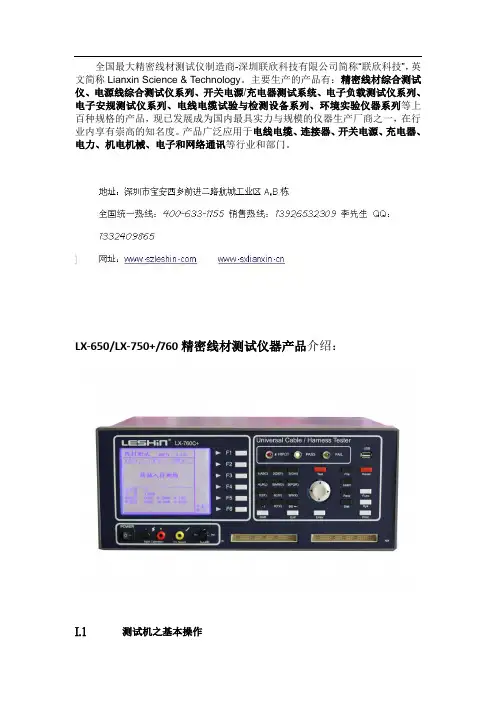
全国最大精密线材测试仪制造商-深圳联欣科技有限公司简称“联欣科技”,英文简称Lianxin Science & Technology。
主要生产的产品有:精密线材综合测试仪、电源线综合测试仪系列、开关电源/充电器测试系统、电子负载测试仪系列、电子安规测试仪系列、电线电缆试验与检测设备系列、环境实验仪器系列等上百种规格的产品,现已发展成为国内最具实力与规模的仪器生产厂商之一,在行业内享有崇高的知名度。
产品广泛应用于电线电缆、连接器、开关电源、充电器、电力、机电机械、电子和网络通讯等行业和部门。
LX-650/LX-750+/760精密线材测试仪器产品介绍:I.1 测试机之基本操作⏹文数字输入在做档案储存时会要求输入文数字,本系统之设计是利用EditKey。
第一次按下为数字,第2~4次分别代表数字键上方由左至右之大写英文字母,举例说明如下:11 2 1A→ 1 1A1 3 1A B⏹移动您可用[←][↑][→][↓]移动光标⏹确认[Enter]为一般之确认键⏹量测/跳离[TEST]为量测激活键,[Exit]为跳离键⏹另选加按[Shift]键可激活该键上方功能I.2 各部位名称I.2.A 前面板(1)LCD液晶显示器(2)S1~S6操作辅助键(SoftKey)(3)控制按键(EditKey)群组(4)PASS & FAIL & H.V. LED(5)量测键[TEST](6)量测快速键群组(7)U盘插入口(8)系统重置(Reset)键(9)系统按键(SysKey)群组(10)图标为128Pin,共有2槽接头(11) 声音调节器(12) Pin Search 接头(点位搜寻) (13) 高压校正输出接头 (14)电源开关I.2.B精密线材测试仪背面板(请参考下图)(1) 串行埠(RS-232 Port) (2) 远程控制埠(Remote Port) (3)打印机连接端口(Printer Port) (4)U 盘插入口(USB )(5)交流电源输入(220V/4A/50Hz) (6)风扇出风口请确认交流输入电压设定与使用电压是否一致。
UL 873Temperature – Indicating and Regulating Equipment温度显示和调节装臵中译本2009.082007.11.161UL 873温度显示和调节装臵标准第1版– 1942.8第2版– 1945.3第3版– 1947.1第4版– 1953.6第5版– 1956.12第6版– 1958.12第7版– 1970.5第8版– 1972.9第9版– 1979.5第10版– 1988.9第11版– 1994.12第12版2007.11.16结构10 调节档板 (27)11 动作机构 (28)12 复位机构-限制控制器 (30)13 调校装臵 (31)性能40 温度试验 (86)41 漏电流试验 (90)42 潮态处理后的漏电流试验 (92)43 操作试验 (93)44 校验试验 (93)45 过载试验 (95)46 耐久性试验 (101)47 介电耐压试验 (104)47.1 概述 (104)47.2 感应电压 (105)47.3 重复感应电压 (106)61 调节档板强度试验 (123)10 调节挡板10.1 由用户操作的、用来限制调节机构的的旋转角度或其移动长度的部件–以下称作调节挡板–其结构在按预期使用方式操作时应能承受61节“调节挡板的强度试验”中的相应试验。
10.2 如果拟在终端产品中使用装臵去限止10.1款所述的调节挡板活动,下述要求适用于终端产品而不是控制器,但:a)如果需要在器具上施加延长手柄等,控制器的调节挡板应有必要的强度以防止在运输和搬运时损坏和改变校验装臵。
b)若控制器没有拟装在器具插头或其它机构里面的调节挡板,在最终装配前应将调节装臵临时密封以减少校验装臵可能的损坏或改变。
c)调节挡板应按照61节“调节挡板强度试验”中的规定试验,但施加在调节装臵上的力矩或力不必大于1磅-英寸(0.1牛.米)或1磅(4.5牛顿)。
11 动作机构11.1 温度指示或恒温装臵的装配结构应保证其不会受到装臵正常动作时产生的振动的影响。
操作图示核准:审核:2013年11月25日制表:周俊杰 1.开启控制箱电源开关,指示灯亮, 2.依照《设备点检保养记录表》点检机器且在表 单项目中记录相应点检结果3.检查放线张力架状态,检查各导轮状况是否良 好,有无破损或运转不灵活现象4.检查各皮带或链条状况是否良好,有没有断裂 5.检查收线轴卡座状态,张开合闭是否灵活 6.依工单及工程图纸设计要求装上相符的铜丝, 将每根铜丝绕过张力架上导轮拉到主机,从主 机上穿线瓷孔及断线感应器孔穿过,7.装好收线轴,启动机器运转调整好排位;8.将铜丝绕在收线轴上,用手转动收线轴3~5圈 让铜丝紧绕在轴上不易松散9.启动主机,自动收线,检查收线排位状况,如 排位不好及时调整10.并丝满轴时按下停止开关,待机器停止运转 后用手抓住铜丝并拉断或剪断,将放线架端的 铜丝绕在机台上的螺丝杆或弹簧上固定好,卸 下并好的铜丝轴,整理好线头并系紧在轴上11.装上空收线轴,将固定在机台上的铜丝绕在收 线轴上重复第8项和第9项操作12.将并好的轴放到指定的装线框里,需按规格 分类放置,不得混在一起以免使用时拿错用错 规格,装线框需有明确的规格标示13.完单后不用的铜丝轴和空轴要卸下,未用完 的铜丝用PE膜包好或装入纸箱放到指定地点14.清理机台内外杂物及油污,清扫周边环境15.关闭主机电源开关 并丝机台操作说明书操作说明图片说明文件编号:SOP-SD-002版本:A0页次:1/1检查放线张力架张力检查各导轮状况,检查皮带或链条状况打开电源总装好铜丝穿过铜丝,绕在收线轴上开启机台量产关闭电源总闸装收线轴,调整排位拆下铜丝,空轴,清扫,清洁 并丝机 电源总闸 指示灯 计量表 开关 开关 计数清零 收线轴固定卡座 断线感应器 穿线瓷孔收线轴 放线张力架 放线张力器 装线框调速开关 过线导轮。
线材测试机作业指导书第一篇:线材测试机是一种用于测试线材质量和性能的专用设备。
在线材的制造和应用领域中,线材测试机起着至关重要的作用。
本篇文章将为大家提供一份线材测试机的作业指导书,帮助大家正确地使用和操作线材测试机。
一、线材测试机的基本原理和结构线材测试机主要通过对线材的物理性能、电学性能和机械性能进行测试,以评估线材的质量和性能指标。
它包括了以下几个主要的测试项目:1.导体电阻测试:测试线材内导体的电阻值,由此评估线材的导电性能和传输能力。
2.绝缘电阻测试:测试线材的绝缘材料对电流的阻隔能力,以确定线材是否存在绝缘缺陷。
3.电容测试:测试线材的电容值,以评估线材的损耗和信号传输效果。
4.屏蔽性能测试:测试线材的屏蔽材料对外界干扰信号的阻隔能力,以确定线材的抗干扰能力。
线材测试机的基本结构包括测试电路、控制系统和显示系统。
测试电路通过接触线材的两端进行电学测试,控制系统负责控制测试过程中的参数和操作,显示系统用于显示测试结果和数据。
二、线材测试机的操作步骤1.准备工作:首先,将线材待测样品进行必要的处理,如去除表面污垢和氧化物。
然后,将待测样品正确接入线材测试机的测试接口。
注意检查接触是否牢固,无松动或断开的情况。
2.选择测试项目:根据测试需求,选择相应的测试项目进行测试。
可以参考线材测试机的使用说明书和相关标准,确定测试项目的参数和要求。
3.设置测试参数:根据测试项目的要求,设置线材测试机的相应参数。
包括测试电流、电压、频率等参数。
确保参数设置正确,以获取准确的测试结果。
4.开始测试:确认设置无误后,开始进行线材测试。
按下测试按钮或触发测试指令,线材测试机将开始进行相应的测试过程。
在测试过程中,注意观察测试指示灯和显示屏,确保测试进行正常。
5.记录和分析测试结果:测试完成后,线材测试机将自动显示测试结果。
将测试结果记录下来,并进行相应的数据分析和比对,以评估线材的质量和性能。
6.报告生成:根据测试结果和数据分析,生成测试报告。
Si873x Data SheetLow Input Current LED Emulator, Logic Output IsolatorsThe Si873x isolators are pin-compatible, single-channel, drop-in replacements for pop-ular optocouplers with data rates up to 15 Mbps. These devices isolate high-speed digital signals and offer performance, reliability, and flexibility advantages not available with optocoupler solutions. The Si873x series is based on Skyworks' proprietary CMOS isolation technology for low-power and high-speed operation and are resistant to the wear-out effects found in optocouplers that degrade performance with increasing tem-perature, forward current, and device age. As a result, the Si873x series offer longer service life and dramatically higher reliability compared to optocouplers. Ordering op-tions include logic output with and without output enable options.Applications•Industrial automation systems •Motor controls and drives •Isolated switch mode power sup-plies •Isolated data acquisition•Test and measurement equipmentSafety Regulatory Approvals•UL 1577 recognized•Up to 2500 V RMS for 1 minute •CSA component notice 5 A appro-val •VDE certification conformity•VDE0884-10 (basic/reinforced insu-lation)•CQC certification approval•GB4943.1KEY FEATURES•High Speed: dc to 15 Mbps•2.5 to 5.5 V logic output•Pin-compatible, drop-in upgrades forpopular high-speed digital optocouplers•Performance and reliability advantages vs.optocouplers:•Resistant to temperature, age andforward current effects•10x lower FIT rate for longer service life•Lower power and forward input diodecurrent•1 channel diode emulator input•Propagation delay 30 ns•10 kV surge withstand capability•AEC-Q100 qualified•Wide operating temperature range: – 40 to+125 °C•RoHS-compliant packages: SOIC-8(Narrow body)OUTSi873x Data Sheet • Ordering Guide1. Ordering GuideTable 1.1. Si873x Ordering Guide1, 2, 3, 4Table of Contents1. Ordering Guide (2)2. Application Information (4)2.1 Theory of Operation (4)3. Functional Description (5)3.1 Device Behavior (5)3.2 Device Startup (5)3.3 Under Voltage Lockout (UVLO) (6)4. Applications (7)4.1 Input Circuit Design (7)4.2 Output Circuit Design and Power Supply Connections (8)5. Electrical Specifications (9)6. Pin Descriptions (SOIC-8) (16)7. Pin Descriptions (SOIC-8) with Output Enable (17)8. Package Outline: 8-Pin Narrow Body SOIC (18)9. Land Pattern: 8-Pin Narrow Body SOIC (20)10. Top Markings (21)10.1 Top Marking: 8-Pin Narrow Body SOIC (21)11. Revision History (22)2. Application Information2.1 Theory of OperationThe Si873x are pin-compatible, single-channel, drop-in replacements for popular optocouplers with data rates up to 15 Mbps. The operation of an Si873x channel is analogous to that of an opto coupler, except an RF carrier is modulated instead of light. This simple architecture provides a robust isolated data path and requires no special considerations or initialization at start-up. A simplified block diagram for the Si873x is shown in the figure below.A BFigure 2.1. Simplified Channel Diagram3. Functional Description3.1 Device BehaviorTruth tables for the Si873x are summarized in the table below.Table 3.1. Si873x Truth Table Summary3.2 Device StartupDuring startup-up, for the Si873x, Output V O is high until V DD rises above the UVLO+ threshold for a minimum time period of t START. Following this, the output is low when the current flowing from anode to cathode is > I F(ON). Device startup, normal operation, and shutdown behavior for the Si873x is shown in the figure below. Note that the figure below assumes that Enable is asserted and that the outputs are operating in their normal operating condition (inverting for the Si8736). See the table above for more details on the Enable function.I F VVIFigure 3.1. Si8736 Operating Behavior (I F > I F(MIN) when V F > V F(MIN))3.3 Under Voltage Lockout (UVLO)The UVLO circuit unconditionally drives V O to its default state when V DD is below the lockout threshold. Referring to the figure below,upon power up, the Si873x is maintained in UVLO until VDD rises above VDD UV+. During power down, the Si873x enters UVLO when VDD falls below the UVLO threshold plus hysteresis (i.e., VDD < VDD UV+ – VDD HYS ).O u t p u t V o l t a g e (V O )Supply Voltage (V DD - GND) (V)Figure 3.2. Si873x UVLO Response4. ApplicationsThe following sections detail the input and output circuits necessary for proper operation of the Si873x family.4.1 Input Circuit DesignOpto coupler manufacturers typically recommend the circuits shown in the figures below. These circuits are specifically designed to improve opto-coupler input common-mode rejection and increase noise immunity.Figure 4.1. Si873x Input CircuitFigure 4.2. High CMR Si873x Input CircuitThe optically-coupled circuit of Figure 4.1 Si873x Input Circuit on page 7 turns the LED on when the control input is high. However, internal capacitive coupling from the LED to the power and ground conductors can momentarily force the LED into its off state when the anode and cathode inputs are subjected to a high common-mode transient. The circuit shown in Figure 4.2 High CMR Si873x Input Circuit on page 7 addresses this issue by using a value of R1 sufficiently low to overdrive the LED, ensuring it remains on during an input common-mode transient. Q1 shorts the LED off in the low output state, again increasing common-mode transient immunity.Some opto coupler applications recommend reverse-biasing the LED when the control input is off to prevent coupled noise from energizing the LED. The Si873x input circuit requires less current and has twice the off-state noise margin compared to opto couplers. However, high CMR opto coupler designs that overdrive the LED (see Figure 4.2 High CMR Si873x Input Circuit on page 7) may require increasing the value of R1 to limit input current I F to its maximum rating when using the Si873x. In addition, there is no benefit in driving the Si873x input diode into reverse bias when in the off state. Consequently, opto coupler circuits using this technique should either leave the negative bias circuitry unpopulated or modify the circuitry (e.g., add a clamp diode or current limiting resistor) to ensure that the anode pin of the Si873x is no more than –0.3 V with respect to the cathode when reverse-biased.New designs should consider the input circuit configurations of Figure 4.3 Si873x Other Input Circuit Configurations on page 8, which are more efficient than those of the figures above. As shown, S1 and S2 represent any suitable switch, such as a BJT or MOSFET, analog transmission gate, processor I/O, etc. Also, note that the Si873x input can be driven from the I/O port of any MCU or FPGA capable of sourcing a minimum of 6 mA (see Figure 4.3 Si873x Other Input Circuit Configurations on page 8C). Additionally, note that the Si873x propagation delay and output drive do not significantly change for values of I F between I F(MIN) and I F(MAX).InputFigure 4.3. Si873x Other Input Circuit Configurations4.2 Output Circuit Design and Power Supply ConnectionsGND can be biased at, above, or below ground as long as the voltage on V DD with respect to GND is a maximum of 5.5 V. V DD decoupling capacitors should be placed as close to the package pins as possible. The optimum values for these capacitors depend on load current and the distance between the chip and its power source. It is recommended that 0.1 and 1 µF bypass capacitors be used to reduce high-frequency noise and maximize performance. Opto replacement applications should limit their supply voltages to 5.5 V or less.5. Electrical SpecificationsTable 5.1. Recommended Operating ConditionsTable 5.2. Electrical CharacteristicsV DD =5 V; GND=0 V; T A =–40 to +125 °C; typical specs at 25 °C1500 ΩFigure 5.1. Diode Emulator Model and I-V CurveFigure 5.2. Common Mode Transient Immunity Characterization CircuitTable 5.3. Regulatory InformationCSA (Pending)The Si873x is certified under CSA Component Acceptance Notice 5A. For more details, see File 232873.VDEThe Si873x is certified according to VDE0884. For more details, see File 5006301-4880-0001.VDE0884-10: Up to 630 V peak for reinforced insulation working voltage.UL (Pending)The Si873x is certified under UL1577 component recognition program. For more details, see File E257455.Rated up to 2500 V RMS isolation voltage for basic protection.CQC (Pending)The Si873x is certified under GB4943.1-2011. For more details, see certificate “pending” yet TBD.Rated up to 130 V RMS reinforced insulation working voltage; up to 600 V RMS basic insulation working voltage. Note: Regulatory Certifications apply to 2.5 kV RMS rated devices which are production tested to 3.0 kV RMS for 1 sec.For more information, see 1. Ordering Guide.Table 5.4. Insulation and Safety-Related SpecificationsTable 5.5. IEC 60664-1 (VDE 0884) RatingsTable 5.6. IEC 60747-5-2 (VDE 0884-10) Insulation CharacteristicsTable 5.7. IEC Safety Limiting ValuesTable 5.8. Thermal Characteristics40060080010001200w e r ‐P s ,I n p u t C u r r e n t ‐I sPs (mW)Is (mA)0200020406080100120140O u t p u t P o Ts ‐Case Temperature (°C)Figure 5.3. (SOIC-8) Thermal Derating Curve, Dependence of Safety Limiting Valueswith Case Temperature per VDE0884-10Table 5.9. Absolute Maximum Ratings6. Pin Descriptions (SOIC-8)NCANODE CATHODENCVDDNCVOSOIC-8Industry Standard PinoutGND Figure 6.1. Pin ConfigurationTable 6.1. Pin Descriptions (SOIC-8, DIP8)7. Pin Descriptions (SOIC-8) with Output EnableNCANODE CATHODENC VDD EN VOSOIC-8 with Output EnableIndustry Standard PinoutGNDFigure 7.1. Pin ConfigurationTable 7.1. Pin Descriptions (SOIC-8, DIP8) with Output EnableSi873x Data Sheet • Pin Descriptions (SOIC-8) with Output Enable8. Package Outline: 8-Pin Narrow Body SOICFigure 8.1 8-Pin Narrow Body SOIC Package on page 18 illustrates the package details for the Si873x in an 8-pin narrow-body SOIC package. Table 8.1 8-Pin Narrow Body SOIC Package Diagram Dimensions on page 18 lists the values for the dimensions shown in the illustration.Figure 8.1. 8-Pin Narrow Body SOIC PackageTable 8.1. 8-Pin Narrow Body SOIC Package Diagram Dimensions9. Land Pattern: 8-Pin Narrow Body SOICThe figure below illustrates the recommended land pattern details for the Si873x in an 8-pin narrow-body SOIC. The table below lists the values for the dimensions shown in the illustration.Figure 9.1. 8-Pin Narrow Body SOIC Land PatternTable 9.1. 8-Pin Narrow Body SOIC Land Pattern Dimensions10. Top Markings10.1 Top Marking: 8-Pin Narrow Body SOICThe figure below illustrates the top markings for the Si873x in an SOIC8 package. The table explains the top marks shown in theillustration.Table 10.1. SOIC8 Top Marking ExplanationLine 1 Marking:Customer Part Number Si87 = Base name of product seriesW = Isolator product series (1 or 2)X = Output configuration5/9 = no enable6 = enable, output high when active7/8 = enable, output Hi-z when active 0 = enable, output low when activeS = Performance Grade:A = 15 Mbps, 20 kV/μs minimum CMTIB = 15 Mbps, 35 kV/μs minimum CMTI V = Insulation ratingC = 3.75 kVLine 2 Marking:RTTTTT = Mfg Code Manufacturing Code from the Assembly Purchase Order form.“R” indicates revision.Line 3 Marking:Circle = 43 mils DiameterLeft-Justified“e4” Pb-Free SymbolYY = YearWW = Work WeekAssigned by the Assembly House. Corresponds to the yearand work week of the mold date.11. Revision HistoryRevision 1.0March, 2018•Initial revision.Copyright © 2021 Skyworks Solutions, Inc. All Rights Reserved.Information in this document is provided in connection with Skyworks Solutions, Inc. (“Skyworks”) products or services. These materials, including the information contained herein, are provided by Skyworks as a service to its customers and may be used for informational purposes only by the customer. Skyworks assumes no responsibility for errors or omissions in these materials or the information contained herein. Skyworks may change its documentation, products, services, specifications or product descriptions at any time, without notice. Skyworks makes no commitment to update the materials or information and shall have no responsibility whatsoever for conflicts, incompatibilities, or other difficulties arising from any future changes.No license, whether express, implied, by estoppel or otherwise, is granted to any intellectual property rights by this document. Skyworks assumes no liability for any materials, products or information provided hereunder, including the sale, distribution, reproduction or use of Skyworks products, information or materials, except as may be provided in Skyworks’ Terms and Conditions of Sale.THE MATERIALS, PRODUCTS AND INFORMATION ARE PROVIDED “AS IS” WITHOUT WARRANTY OF ANY KIND, WHETHER EXPRESS, IMPLIED, STATUTORY, OR OTHERWISE, INCLUDING FITNESS FOR A PARTICULAR PURPOSE OR USE, MERCHANTABILITY, PERFORMANCE, QUALITY OR NON-INFRINGEMENT OF ANY INTELLECTUAL PROPERTY RIGHT; ALL SUCH WARRANTIES ARE HEREBY EXPRESSLY DISCLAIMED. SKYWORKS DOES NOT WARRANT THE ACCURACY OR COMPLETENESS OF THE INFORMATION, TEXT, GRAPHICS OR OTHER ITEMS CONTAINED WITHIN THESE MATERIALS. SKYWORKS SHALL NOT BE LIABLE FOR ANY DAMAGES, INCLUDING BUT NOT LIMITED TO ANY SPECIAL, INDIRECT, INCIDENTAL, STATUTORY, OR CONSEQUENTIAL DAMAGES, INCLUDING WITHOUT LIMITATION, LOST REVENUES OR LOST PROFITS THAT MAY RESULT FROM THE USE OF THE MATERIALS OR INFORMATION, WHETHER OR NOT THE RECIPIENT OF MATERIALS HAS BEEN ADVISED OF THE POSSIBILITY OF SUCH DAMAGE.Skyworks products are not intended for use in medical, lifesaving or life-sustaining applications, or other equipment in which the failure of the Skyworks products could lead to personal injury, death, physical or environmental damage. Skyworks customers using or selling Skyworks products for use in such applications do so at their own risk and agree to fully indemnify Skyworks for any damages resulting from such improper use or sale.Customers are responsible for their products and applications using Skyworks products, which may deviate from published specifications as a result of design defects, errors, or operation of products outside of published parameters or design specifications. Customers should include design and operating safeguards to minimize these and other risks. Skyworks assumes no liability for applications assistance, customer product design, or damage to any equipment resulting from the use of Skyworks products outside of Skyworks’ published specifications or parameters.Skyworks, the Skyworks symbol, Sky5®, SkyOne ®, SkyBlue™, Skyworks Green™, Clockbuilder ®, DSPLL ®, ISOmodem ®, ProSLIC ®, and SiPHY ® are trademarks or registered trademarks of Skyworks Solutions, Inc. or its subsidiaries in the United States and other countries. Third-party brands and names are for identification purposes only and are the property of their respective owners. Additional information, including relevant terms and conditions, posted at , are incorporated by reference.PortfolioQuality/qualitySupport & Resources/support。