电路分析答案内容第三章
- 格式:doc
- 大小:1.16 MB
- 文档页数:12
CHAPTER 3P3.1. The general approach for the first two parameters is to figure out which variables shouldremain constant, so that when you have two currents, you can divide them, and every variable but the ones you want to calculate remain. In this case, since the long-channel transistor is in saturation for all values of V GS and V DS , only one equation needs to be considered:()()2112DS N OX GS T DS W I C V V V Lμλ=-+ For the last two parameters, now that you have enough values, you can just choose oneset of numbers to compute their final values.a. The threshold voltage, V T0, can be found by choosing two sets of numbers with the same V DS ’s but with different V GS ’s. In this case, the first two values in the table can be used.()()()()()()211122222201022001121121.2 1.210000.82800.8DS N OX GS T DS DS N OX GS T DS T DS T DS T T W I C V V V L W I C V V V LV I V I V V μλμλ=-+=-+-⎛⎫-===⎪--⎝⎭ 00.35V T V ∴=b. The channel modulation parameter, λ, can be found by choosing two sets of numberswith the same V GS ’s but with different V DS ’s. In this case, the second and third values in the table can be used.()()221 1.225010.8247DS DS I I λλ+==+ -10.04V λ∴=c. The electron mobility, µn , can now be calculated by looking at any of the first three sets of numbers, but first, let’s calculate C OX .631062-31m 10μm22?.210μm1m 10 0.0351 1.610/2.210OX OX t C F cm--=⨯⨯===⨯Now calculate the mobility by using the first set of numbers.()()()()()()()()()()()()22111021262101111 1.21 1.222210002cm 348V-s 1.610(4.75)1.20.3510.04 1.21DS N OX GS T DS N OX T DS N OX GS T DS W W I C V V V C V L LA I W C V V V L μλμλμμλ-=-+=-+===⨯-+-+d. The body effect coefficient gamma, γ, can be calculated by using the last set of numbers since it is the only one that has a V SB greater than 0V.()()()()244124414411221 1.20.468VDS N OX GS T DS DS GS T N OX DS GS T T GS W I C V V V LI V V W C V LV V V V μλμλ=-+-=+-==-==12000.6VT T T T V V V V γγγ=+-====P3.2. The key to this question is to identify the transistor’s region of operation so that gatecapacitance may be assigned appropriately, and the primary capacitor that will dischargedat a rate of V It C ∂∂= by the current source may be identified. Then, because the nodes arechanging, the next region of operation must be identified. This process continues until the transistor reaches steady state behavior. Region 1:Since 0V GS V = the transistor is in the cutoff region. The gate capacitance is allocated to GB C . Since no current will flow through the transistor, all current will come from the source capacitor and the drain node remains unchanged.68-151010V V 6.67100.6671510s nsSB V I I t C C -∆⨯====⨯=∆⨯ The source capacitor will discharge until 1.1V GS T V V == when the transistor enters thesaturation region. This would require that the source node would be at 3.3 1.1 2.2V S G GS V V V =-=-=.()15961510 3.3 2.2 1.6510s 1.65ns 1010C t V I ---⨯∆=∆=-=⨯=⨯ Region 2:The transistor turns on and is in saturation. The current is provided from the capacitor atthe drain node, while the source node remains fairly constant. The capacitance at the drain node is the same as the source node so the rate of change is given by:68-151010V V 6.67100.6671510s nsSB V I I t C C -∆⨯====⨯=∆⨯ Since the transistor is now in the saturation region, GS V can be computed based on thecurrent flowing through the device.()22 1.1 1.37V 3.3 1.37 1.93VGS T GST S G GS kW I V V LV V V V V =-==+==-=-=This is where the source node settles. This means that most of the current is discharged through the transistor until the drain voltage reaches a value that puts the transistor at the edge of saturation.3.3 1.1 2.2VDS GS TD G T V V V V V V =-=-=-=If we assume that all the current comes from the transistor, and the source node remains fixed, the drain node will then discharge at a rate equal to that of the source node in the first region. Region 3:The transistor is now in the linear region the gate capacitance is distributed equally to both GS C and GD C . and both capacitors will discharge at approximately the same rate.-151510V0.28621510510nsV I A t C μ-∆===∆⨯⨯+⨯The graph is shown below.00.511.522.533.5024681012Time (ns)V o l t a g e (V )P3.3. The gate and drain are connected together so that DS GS V V = which will cause thetransistor to remain in saturation. This is a dc measurement so capacitances are not required. Connect the bulk to ground and run SPICE. P3.4. Run SPICE. P3.5. Run SPICE. P3.6. Run SPICE. P3.7. Run SPICE.P3.8. First, let’s look at the various parameters and identify how they affect V T .∙ L – Shorter lengths result in a lower threshold voltage due to DIBL. ∙ W – Narrow width can increase the threshold voltage.∙ V SB – Larger source-bulk voltages (in magnitude) result in a higher threshold voltage. ∙ V DS –Larger drain-source voltages (in magnitude) result in a lower threshold voltage due to DIBL. The transistor with the lowest threshold voltage has the shortest channel, larger width, smallest source-bulk voltage and largest drain-source voltage. This would be the first transistor listed.The transistor with the highest threshold voltage has the longest channel, smallest width,largest source-bulk voltage and smallest drain-source voltage. This would be the last transistor listed. P3.9. Run SPICE.P3.10. Run SPICE. The mobility degradation at high temperatures reduces I on and the increasemobile carriers at high temperatures increase I off . P3.11. The issues that prompted the switch from Al to Cu are resistance and electromigration.Copper wires have lower resistances and are less susceptible to electromigration problems. Copper on the other hand, reacts with the oxygen in SiO 2 and requires cladding around the wires to prevent this reaction.For low-k dielectrics, the target value future technologies is 2.High-k dielectrics are being developed as the gate-insulator material of MOSFET’s. This is because the current insulator material, SiO 2, can not be scaled any longer due to tunneling effects.P3.12. Self-aligned poly gates are fabricated by depositing oxide and poly before the source anddrain regions are implanted. Self-aligned silicides (salicides) are deposited on top of the source and drain regions using the spacers on the sides of the poly gate. P3.13. To compute the length, simply use the wire resistance equation and solve for L .LR TWRTWL ρρ==First convert the units of ρ to terms of μm. Aluminum:2.7μΩρ=cm 6Ω10μΩ⨯610μm100cm ⨯()()()0.027Ωμm1000.812963μm 2.96mm0.027RTWL ρ=====Copper:1.7μΩρ=cm 6Ω10μΩ⨯610μm100cm ⨯()()()0.017Ωμm1000.814706μm 4.71mm0.017RTWL ρ=====P3.14. Generally, the capacitance equation in terms of permittivity constants and spacing is:k C WL tε=a. 4k = ()()()()230048.8510 3.541100SiO k k C WL TL t S S Sεε-====b. 2k = ()()()()30028.8510 1.771100k k C WL TL t S SSεε-====The plots are shown below.Capacitance vs. Spacing01234567800.511.522.533.544.555.5Spacing (um)C a p a c i t a n c e (f F)。
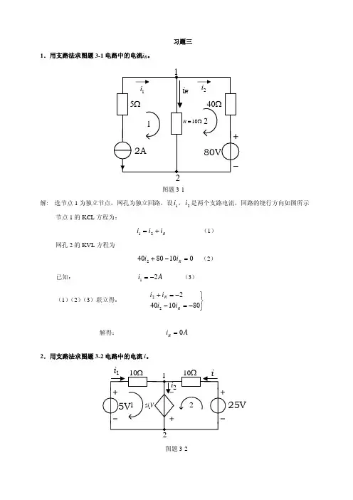
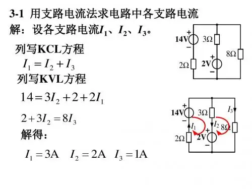
第三章电阻电路的一般分析电路的一般分析是指方程分析法,它是以电路元件的约束特性(VCR)和电路的拓扑约束特性(KCL,KVL)为依据,建立以支路电流或回路电流,或结点电压为变量的回路方程组,从中解出所要求的电流、电压、功率等。
方程分析法的特点是:(1)具有普遍适用性,即无论线性和非线性电路都适用;(2)具有系统性,表现在不改变电路结构,应用KCL,KVL,元件的VCR建立电路变量方程,方程的建立有一套固定不变的步骤和格式,便于编程和用计算机计算。
本章的重点是会用观察电路的方法,熟练运用支路法、回路法和结点电压法的“方程通式”写出支路电流方程、回路方程和结点电压方程,并加以求解。
3-1 在一下两种情况下,画出图示电路的图,并说明其节点数和支路数(1)每个元件作为一条支路处理;(2)电压源(独立或受控)和电阻的串联组合,电流源和电阻的并联组合作为一条支路处理。
解:(1)每个元件作为一条支路处理时,图(a)和(b)所示电路的图分别为题解3-1图(a1)和(b1)。
图(a1)中节点数6b==n,支路数11图(b1)中节点数7b==n,支路数12(2)电压源和电阻的串联组合,电流源和电阻的并联组合作为一条支路处理时,图(a)和图(b)所示电路的图分别为题解图(a2)和(b2)。
图(a2)中节点数4b=n,支路数8=图(b2)中节点数15n,支路数9=b=3-2指出题3-1中两种情况下,KCL,KVL独立方程数各为多少?解:题3-1中的图(a)电路,在两种情况下,独立的KCL方程数分别为(1)51=-4-n1==61=-1-n(2)3独立的KVL方程数分别为(1)641=8-b1-n+=+1=111b(2)5+6+--n=图(b)电路在两种情况下,独立的KCL方程数为(1)651=-=1-n7-n(2)41=1-=独立的KVL方程数分别为(1)6+1=95b1-n+=-=12711=+-nb(2)5+-3-3对题图(a)和(b)所示G,各画出4个不同的树,树支数各为多少?解:一个连通图G的树T是这样定义的:(1) T包含G的全部结点和部分支路;(2) T本身是连通的且又不包含回路。
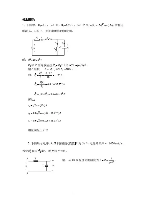
相量图形:1、下图中,R 1=6Ω,L=0.3H ,R 2=6.25Ω,C=0.012F,u (t)=)10cos(210t ,求稳态电流i 1、i 2和i 3,并画出电路的相量图。
解:V U0010∠= R 2和C 的并联阻抗Z 1= R 2//(1/j ωC )=(4-j3)Ω, 输入阻抗 Z = R 1+j ωL +Z 1 =10Ω,则:A Z U I 0010110010∠=∠== A R Z I I 0211287.368.0-∠== A U C j I 02313.536.0∠== ω 所以:A t i )10cos(21=A t i )87.3610cos(28.02ο-= A t i )13.5310cos(26.02ο+=相量图见上右图2、下图所示电路,A 、B 间的阻抗模值Z 为5k Ω,电源角频率ω=1000rad/s ,为使1U 超前2U 300,求R 和C 的值。
解:从AB 端看进去的阻抗为Cj R Z ω1+=, I213其模值为:Ω=+=k CR Z 5)1(22ω (1) 而2U /1U =)arctan()(112CR CR ωω-∠+由于1U 超前2U 300,所以ωCR =tan300=31 (2)联列(1)、(2)两式得R =2.5k Ω,C =0.231μF3、测量阻抗Z 的电路如下图所示。
已知R=20Ω,R 2=6.5Ω,在工频(f =50Hz)下,当调节触点c 使R ac =5Ω时,电压表的读数最小,其值为30V ,此时电源电压为100V 。
试求Z 及其组成的元件的参数值。
(注意:调节触点c ,只能改变cd U 的实部,电压表读数最小,也就是使实部为零,cd U 为纯虚数,即cdU =±j30V)解:UZR R U R R U ac cd++-=22调节触点c ,只能改变cd U 的实部,其值最小,也就是使实部为零,cd U 为纯虚数,即cdU =±j30V , 因此上式可表示为:±j 30=-25+(100⨯6.5)/(6.5+Z ) 解得:Z=(4.15±j 12.79)Ω 故:R Z =4.15ΩL =40.7mHC =249μF4、电路如下图所示,已知f =1kHz ,U =10V ,U 1=4V ,U 2=8V 。
第三章 电阻电路的一般分析一、是非题 (注:请在每小题后[ ]内用"√"表示对,用"×"表示错).1. 利用节点KCL方程求解某一支路电流时,若改变接在同一节点所有其它已知支路电流的参考方向,将使求得的结果有符号的差别。
[×] .2. 列写KVL方程时,每次一定要包含一条新支路才能保证方程的独立性。
[√] .3. 若电路有n个节点,按不同节点列写的n-1个KCL方程必然相互独立。
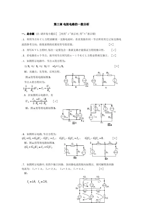
[√] .4. 如图所示电路中,节点A的方程为: (1/R 1 +1/ R 2 +1/ R 3)U =I S +US /R 3 [×]解:关键点:先等效,后列方程。
图A 的等效电路如图B :节点A的方程应为: 332)11(R U I U R R S S A +=+ .5. 在如图所示电路中, 有 12232/1/1/S S A I U R U R R +=+ [√]解:图A 的等效电路如图B :.6. 如图所示电路,节点方程为:12311()S S G G G U GU I ++-=; 3231S G U G U I -=; 13110GU GU -=. [×]解:图A 的等效电路如图B :S S U G I U G G 1121)(+=+.7. 如图所示电路中,有四个独立回路。
各回路电流的取向如图示, 则可解得各回路 电流为: I1=1A;I2=2A; I3=3A;I4=4A。
[×] 解:;11A I = ;22A I =;33A I = ;7344A I =+=二、选择题(注:在每小题的备选答案中选择适合的答案编号填入该题空白处,多选或不选按选错论).1.对如图所示电路,下列各式求支路电流正确的是 C_。
(A) 12112E E I R R -=+; (B) 222E I R =(C) AB L LUI R =.2. 若网络有b 条支路、n 个节点,其独立KCL方程有_C_个,独立KVL方程有_D__个,共计为_A_个方程。
第三章双极型三极管基本放大电路3-1 选择填空1.晶体管工作在放大区时,具有如下特点______________。
a. 发射结正偏,集电结反偏。
b. 发射结反偏,集电结正偏。
c. 发射结正偏,集电结正偏。
d. 发射结反偏,集电结反偏。
2.晶体管工作在饱和区时,具有如下特点______________。
a. 发射结正偏,集电结反偏。
b. 发射结反偏,集电结正偏。
c. 发射结正偏,集电结正偏。
d. 发射结反偏,集电结反偏。
3.在共射、共集、共基三种基本组态放大电路中,电压放大倍数小于1的是______组态。
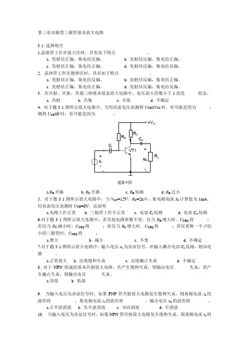
a. 共射b. 共集c. 共基d. 不确定4.对于题3-1图所示放大电路中,当用直流电压表测得U CE ≈V CC 时,有可能是因为______,测得U CE ≈0时,有可能是因为________。
题3-1图ccR La.R B 开路b. R C 开路c. R B 短路d. R B 过小5.对于题3-1图所示放大电路中,当V CC =12V ,R C =2k Ω,集电极电流I C 计算值为1mA 。
用直流电压表测时U CE =8V ,这说明______。
a.电路工作正常b. 三极管工作不正常c. 电容C i 短路d. 电容C o 短路 6.对于题3-1图所示放大电路中,若其他电路参数不变,仅当R B 增大时,U CEQ 将______;若仅当R C 减小时,U CEQ 将______;若仅当R L 增大时,U CEQ 将______;若仅更换一个β较小的三极管时,U CEQ 将______;a.增大b. 减小 c . 不变 d. 不确定 7.对于题3-1图所示放大电路中,输入电压u i 为余弦信号,若输入耦合电容C i 短路,则该电路______。
a.正常放大b. 出现饱和失真c. 出现截止失真d. 不确定 8. 对于NPN 组成的基本共射放大电路,若产生饱和失真,则输出电压_______失真;若产生截止失真,则输出电压_______失真。
电路分析基础习题第三章答案(史健芳)第3章3.1 选择题1.必须设立电路参考点后才能求解电路的方法是( C )。
A.支路电流法B.回路电流法C.节点电压法D.2b法2.对于一个具有n个结点、b条支路的电路,他的KVL独立方程数为( B )个。
A.n-1 B.b-n+1 C.b-nD.b-n-13.对于一个具有n个结点、b条支路的电路列写结点电压方程,需要列写( C )。
A.(n-1)个KVL方程B.(b-n+1)个KCL方程C.(n-1)个KCL方程D.(b-n-1)个KCL方程4.对于结点电压法中的无伴电压源,下列叙述中,( A )是错误的。
A.可利用电源等效变换转化为电流源后,再列写结点电压方程B.可选择该无伴电压源的负极性端为参考结点,则该无伴电压源正极性端对应的结点电压为已知,可少列一个方程C.可添加流过该无伴电压源电流这一新的未知量,只需多列一个该无伴电压源电压与结点电压之间关系的辅助方程即可D.无伴受控电压源可先当作独立电压源处理,列写结点电压方程,再添加用结点电压表示控制量的补充方程5.对于回路电流法中的电流源,下列叙述中,( D )是错误的。
A.对于有伴电流源,可利用电源等效变换转化为电压源后,再列写回路电流方程B.对于无伴电流源,可选择合适的回路,使只有一个回路电流流过该无伴电流源,则该回路电流为已知,可少列一个方程C.对于无伴电流源,可添加该无伴电流源两端电压这一新的未知量,只需多列一个无伴电流源电流与回路电流之间关系的辅助方程即可D.电流源两端的电压通常为零6.对于含有受控源的电路,下列叙述中,( D )是错误的。
A.受控源可先当作独立电源处理,列写电路方程B.在结点电压法中,当受控源的控制量不是结点电压时,需要添加用结点电压表示控制量的补充方程C.在回路电流法中,当受控源的控制量不是回路电流时,需要添加用回路电流表示控制量的补充方程D.若采用回路电流法,对列写的方程进行化简,在最终的表达式中互阻始终是相等的,即:R ij=R ji3.2 填空题1.对于具有n个结点b条支路的电路,可列出 n-1 个独立的KCL方程,可列出 b-n+1 个独立的KVL方程。
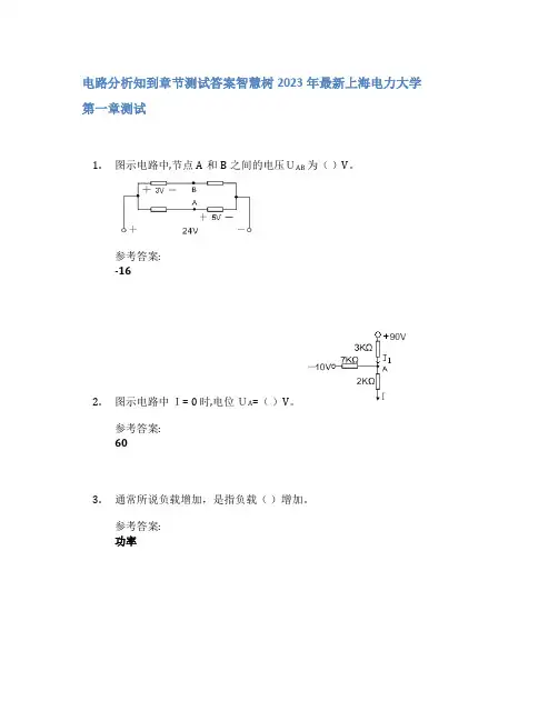
电路分析知到章节测试答案智慧树2023年最新上海电力大学第一章测试1.图示电路中,节点A和B之间的电压UAB为()V。
参考答案:-162.图示电路中I= 0 时,电位UA=()V。
参考答案:603.通常所说负载增加,是指负载()增加。
参考答案:功率4.图示电路中S断开时I1= 0A,I=2A。
S闭合时I1=( )A,I=( )A。
()参考答案:0;65.图示电路中,当IS=10A 时,电压U为()V,当IS=8A时电压U为()V。
()参考答案:12;166.电路理论分析的对象是电路模型而不是实际电路。
()参考答案:对7.欧姆定律可表示成U=RI,也可表示成U=-RI,这与采用的参考方向有关。
()参考答案:对8.在节点处各支路电流的方向不能均设为流向节点,否则将只有流入节点的电流而无流出节点的电流。
()参考答案:错9.在电压近似不变的供电系统中,负载增加相当于负载电阻减少。
()参考答案:对10.理想电压源的端电压是由它本身确定的,与外电路无关,因此流过它的电流则是一定的,也与外电路无关。
()参考答案:错第二章测试1.图示电路AB间的等效电阻为()。
参考答案:14Ω2.电路如图所示,A、B端的等效电阻R=()。
参考答案:4Ω3.电路如图所示,可化简为()参考答案:3Ω电阻4.如图所示电路中,当电阻R2增加时电流I将()。
参考答案:增加5.图示电路中,就其外特性而言,()。
参考答案:b、c等效6.两只额定电压为110V的电灯泡串联起来总可以接到220V的电压源上使用。
()参考答案:错7.电流相等的两个元件必属串联,电压相等的两个元件必属并联。
()参考答案:错8.一个不含独立源的电阻性线性二端网络(可以含受控源)总可以等效为一个线性电阻。
()参考答案:对9.一个含独立源的电阻性线性二端网络(可以含受控源)总可以等效为一个电压源与一个电阻串联或一个电流源与一个电阻并联。
()参考答案:对10.已知图示电路中A、B两点电位相等,则AB支路中必然电流为零。
电路如题图3 — I 所示。
(1)用叠加定理计算电流I 。
⑵ 欲使I =0,问U S 应改为何值。
18V“2A 3门 6门 1A- 61'.1§ 3— 1叠加定理解: 得CD(a)和图(b)所示。
由此求I(2)由以上计算结果得到下式-3A1=11U S 1A - 0 Us =「(9」)1A--9V3—2用叠加定理求题图 3—2电路中电压U题图3 — 2 解:画出独立电流源和独立电压源分别单独作用的电路如图(a)和图(b)所示。
由此求得4=3£/a =l8V |题图3 — 1(1)画出独立电压源和独立电流源分别单独作用的电路如图 +s=isv ()ODia5—^6 8V = 4V21「36门 3 + 6"— - 3 "”i12cos3t =-5cos3tAu = -(21) i =10cos3tV5 [□ 2 3l 丿 2+3i =i i =(2「5cos3t)Au =u u =(4 10cos3t)V3-4用叠加定理求题图 3-4电路中的电流i 和电压u 。
⑷题图3 — 4 解:画出独立电压源和独立电流源分别单独作用的电路如图(a)和图(b)所示。
由此求得U ' - 3A 3;. ; -5V50+(10+30) "3;' U 9V =3V60 +3。
)亠 2A2 门 36'J 3+6列出图(a)电路KVL方程(■」3「)i' 2u1 -6V =0'6V ' 'i 1A u =—3门i =—3Vi" 2u;3门(i" -4A) =03-6用叠加定理求题图3-6电路中电流i 。
解:画出12V和18V独立电压源单独作用的电路如图-18Vo 30汇40 3小60 103103'130+40i =i' i"二0.2mA -0.1mA = 0.1mA代入u1』i"得到―罟①最后得到i =i'订"=1A・2A =3Au" =3 门(4A-i")=6Vu = u u = -3V 6V = 3+ 12V4okn题图3 —6(=)3—7用叠加定理求题图3—7单口网络的电压电流关系。
电路分析第五版答案第一章:基本概念和电路定律练习题答案a.看图1.1.CircuitCircuitb.从图中可以看出,电流I分为两个路径,通过电阻R1和R2。
根据欧姆定律,我们可以计算出电流I的值。
从电源V1开始,沿着电流的流向,电流经过电阻R1,其电压降为V1 - I R1。
然后经过电阻R2,其电压降为(V1 - I R1) - I * R2。
根据基尔霍夫电压定律,这个电压降等于电源的电压V1。
所以我们可以得到方程(V1 - I*R1) - I * R2 = V1。
通过解这个方程,我们可以计算出电流I的值。
a.如果电流经过电阻R1和电流源I1,那么根据欧姆定律,我们可以得到电流I1的值为I1 = V1 / R1。
b.如果电流经过电流源I2,则根据欧姆定律,我们可以得到电流I2的值为I2 = V2 / R2。
c.根据基尔霍夫电流定律,两个电流源的总和等于流入节点的电流总和。
所以我们可以得到I1 + I2 = I。
综上所述,我们得到了电路中的电流和电阻之间的关系。
第二章:电路简化技术练习题答案a.直接串联与并联等效电阻的计算公式为:–直接串联:R = R1 + R2 + R3 + ...–直接并联:1 / R = 1 / R1 + 1 / R2 + 1 / R3 + ...b.根据以上公式,我们可以计算出串联和并联电路的等效电阻。
a.并联电路等效电阻的计算公式为:1 / R = 1/ R1 + 1 / R2。
b.代入R1=4欧姆和R2=5欧姆的值,我们可以计算得到1 / R = 1 / 4 + 1 / 5。
进一步计算可得1 / R = 0.45。
最后,通过倒数运算可以得到R= 2.22欧姆。
所以,电路中的等效电阻为2.22欧姆。
实验题答案a.看图2.1.Simplified CircuitSimplified Circuitb.根据电路简化技术,我们可以将电感L1和L2合并,并求得等效电感L。
通过串联和并联电感的公式,我们可以得到等效电感的计算公式:L = L1 + L2。
电路分析基础第一章一、1、电路如图所示, 其中电流I 1为 答( A ) A 0.6 AB. 0.4 AC. 3.6 AD. 2.4 A3Ω6Ω2、电路如图示, U ab 应为 答 ( C )A. 0 VB. -16 VC. 0 VD. 4 V3、电路如图所示, 若R 、U S 、I S 均大于零,, 则电路的功率情况为 答( B ) A. 电阻吸收功率, 电压源与电流源供出功率 B. 电阻与电流源吸收功率, 电压源供出功率 C. 电阻与电压源吸收功率, 电流源供出功率 D. 电阻吸收功率,供出功率无法确定UI S二、 1、图示电路中, 欲使支路电压之比U U 122=,试确定电流源I S 之值。
I SU解:I S由KCL 定律得:22328222U U U ++=U 24811=V由KCL 定律得:0422=++U I U S1160-=S I A 或-5.46 A 2、用叠加定理求解图示电路中支路电流I ,可得:2 A 电流源单独作用时,I '=2/3A;4 A 电流源单独作用时, I "=-2A, 则两电源共同作用时I =-4/3A 。
3、图示电路ab 端的戴维南等效电阻R o = 4 Ω;开路电压U oc = 22 V 。
ba2解:U=2*1=2 I=U+3U=8A Uab=U+2*I+4=22V Ro=4Ω第二章一、1、图示电路中,7 V 电压源吸收功率为 答 ( C )A. 14 WB. -7 WC. -14 WD. 7 W2、图示电路在t =0时开关闭合,t ≥0时u t C ()为 答 (D )A. ---1001100(e )V tB. (e )V -+-505050tC. --100100e V tD. ---501100(e )V tu C3、图示桥式电路中,已知t U u ωcos m s =,欲使图中u =0,应满足的条件为 答( A )A.C L R R =21 B.LC R R 221ω=C. CR L R ωω21=D. CR L R ωω12=2u二、 1、试用叠加定理求图示电路中的电压U 。