MAX809中文资料_数据手册_参数
- 格式:pdf
- 大小:188.96 KB
- 文档页数:13
General Description The MAX803/MAX809/MAX810 are microprocessor (µP) supervisory circuits used to monitor the power supplies in µP and digital systems. They provide excellent circuit reliability and low cost by eliminating external compo-nents and adjustments when used with +5V, +3.3V, +3.0V, or +2.5V-powered circuits.These circuits perform a single function: they assert a reset signal whenever the V CC supply voltage declines below a preset threshold, keeping it asserted for at least 140ms after V CC has risen above the reset thresh-old. Reset thresholds suitable for operation with a vari-ety of supply voltages are available.The MAX803 has an open-drain output stage, while the MAX809/MAX810 have push-pull outputs. The MAX803’s open-drain RESET output requires a pull-up resistor that can be connected to a voltage higher than V CC. The MAX803/MAX809 have an active-low RESET output, while the MAX810 has an active-high RESET output. The reset comparator is designed to ignore fast transients on V CC, and the outputs are guaranteed to be in the correct logic state for V CC down to 1V.Low supply current makes the MAX803/MAX809/ MAX810 ideal for use in portable equipment. The MAX803 is available in a 3-pin SC70 package, and the MAX809/MAX810 are available in 3-pin SC70 or SOT23 packages.Applications ComputersControllersIntelligent InstrumentsCritical µP and µC Power MonitoringPortable/Battery-Powered EquipmentAutomotive ____________________________Features o Precision Monitoring of +2.5V, +3V, +3.3V, and +5V Power-Supply Voltageso Fully Specified Over Temperatureo Available in Three Output ConfigurationsOpen-Drain RESET Output (MAX803)Push-Pull RESET Output (MAX809)Push-Pull RESET Output (MAX810)o140ms min Power-On Reset Pulse Widtho12µA Supply Currento Guaranteed Reset Valid to V CC= +1Vo Power Supply Transient Immunityo No External Components o3-Pin SC70 and SOT23 Packages MAX803L/M/R/S/T/Z, MAX809J/L/M/R/S/T/Z, MAX810L/M/R/S/T/Z3-Pin Microprocessor Reset Circuits________________________________________________________________Maxim Integrated Products1Pin Configuration Typical Operating Circuit19-0344; Rev 4; 12/99Note: These parts are offered in 2.5k or 10k reels, and must beordered in 2.5k or 10k increments. Order MAX803_EXR-T for2.5k reels and MAX803_EXR-T10 for 10k reels. Insert thedesired suffix letter from the Selector Guide into the blank tocomplete the part number. All versions of these products maynot be available at the time of announcement. Contact factory foravailability.For free samples & the latest literature: , or phone 1-800-998-8800. For small orders, phone 1-800-835-8769.Ordering InformationM A X 803L /M /R /S /T /Z , M A X 809J /L /M /R /S /T /Z , M A X 810L /M /R /S /T /Z3-Pin Microprocessor Reset CircuitsABSOLUTE MAXIMUM RATINGSELECTRICAL CHARACTERISTICS(V CC = full range, T A = -40°C to +105°C, unless otherwise noted. Typical values are at T A = +25°C, V CC = 5V for L/M/J versions, V CC = 3.3V for T/S versions, V CC = 3V for R version, and V CC = 2.5V for Z version.) (Note 1)Stresses beyond those listed under “Absolute Maximum Ratings” may cause permanent damage to the device. These are stress ratings only, and functional operation of the device at these or any other conditions beyond those indicated in the operational sections of the specifications is not implied. Exposure to absolute maximum rating conditions for extended periods may affect device reliability.Terminal Voltage (with respect to GND)V CC ....................................................................-0.3V to +6.0V RESET, RESET (push-pull).....................-0.3V to (V CC + 0.3V)RESET (open drain)...........................................-0.3V to +6.0V Input Current, V CC ..............................................................20mA Output Current, RESET, RESET ..........................................20mA Rate of Rise, V CC ............................................................100V/µsContinuous Power Dissipation (T A = +70°C)3-Pin SC70 (derate 2.17mW/°C above +70°C)............174mW 3-Pin SOT23 (derate 4mW/°C above +70°C)...............320mW Operating Temperature Range .........................-40°C to +105°C Storage Temperature Range.............................-65°C to +150°C Lead Temperature (soldering, 10s).................................+300°CMAX803L/M/R/S/T/Z, MAX809J/L/M/R/S/T/Z, MAX810L/M/R/S/T/Z3-Pin Microprocessor Reset Circuits_______________________________________________________________________________________3A Note 2:RESET output for MAX803/MAX809; RESET output for MAX810.POWER-DOWN RESET DELAY vs. TEMPERATURE (MAX8_ _R/S/T/Z)80100TEMPERATURE (°C)P O W E R -D O W N R E S E T D E L A Y (µs )402060-408520-2006040Typical Operating Characteristics(V CC = full range, T A = -40°C to +105°C, unless otherwise noted. Typical values are at T A = +25°C, V CC = +5V for L/M/J versions,V CC = +3.3V for T/S versions, V CC = +3V for R version, and V CC = +2.5V for Z version.)ELECTRICAL CHARACTERISTICS (continued)(V CC = full range, T A = -40°C to +105°C, unless otherwise noted. Typical values are at T A = +25°C, V CC = 5V for L/M/J versions, V CC = 3.3V for T/S versions, V CC = 3V for R version, and V CC = 2.5V for Z version.) (Note 1)-402040-206085SUPPLY CURRENT vs. TEMPERATURE(SC70 PACKAGE, NO LOAD)TEMPERATURE (°C)S U P P L Y C U R R E N T (µA )051015M A X 803L /M /R /S /T /Z , M A X 809J /L /M /R /S /T /Z , M A X 810L /M /R /S /T /Z3-Pin Microprocessor Reset Circuits 4_______________________________________________________________________________________Typical Operating Characteristics (continued)(V CC = full range, T A = -40°C to +105°C, unless otherwise noted. Typical values are at T A = +25°C, V CC = +5V for L/M/J versions,V CC = +3.3V for T/S versions, V CC = +3V for R version, and V CC = +2.5V for Z version.)225POWER-UP RESET TIMEOUTvs. TEMPERATURE245250TEMPERATURE (°C)P O W E R -U P R E S E T T I M E O U T (m s )235230240-408520-2060400.997NORMALIZED RESET THRESHOLDvs. TEMPERATURE1.0011.0021.003M A X 803-T O C 6TEMPERATURE (°C)N O R M A L I Z E D T H R E S H O L D0.9990.9981.000-408520-206040Selector Guide0POWER-DOWN RESET DELAY vs. TEMPERATURE (MAX8_ _J/L/M)80100120140TEMPERATURE (°C)P O W E R -D O W N R E S E T D E L A Y (µs )402060-408520-2006040MAX803L/M/R/S/T/Z, MAX809J/L/M/R/S/T/Z, MAX810L/M/R/S/T/Z_______________________________________________________________________________________5Detailed DescriptionA microprocessor’s (µP’s) reset input starts the µP in a known state. The MAX803/MAX809/MAX810 assert reset to prevent code-execution errors during power-up, power-down, or brownout conditions. They assert a reset signal whenever the V CC supply voltage declines below a preset threshold, keeping it asserted for at least 140ms after V CC has risen above the reset thresh-old. The MAX803 uses an open-drain output, and the MAX809/MAX810 have a push-pull output stage.Connect a pull-up resistor on the MAX803’s RESET out-put to any supply between 0 and 6V.Applications InformationNegative-Going V CC TransientsIn addition to issuing a reset to the µP during power-up,power-down, and brownout conditions, the MAX803/MAX809/MAX810 are relatively immune to short-duration negative-going V CC transients (glitches).Figure 1 shows typical transient duration vs. reset com-parator overdrive, for which the MAX803/MAX809/MAX810 do not generate a reset pulse. The graph was generated using a negative-going pulse applied to V CC ,starting 0.5V above the actual reset threshold and end-ing below it by the magnitude indicated (reset compara-tor overdrive). The graph indicates the maximum pulse width a negative-going V CC transient can have without causing a reset pulse. As the magnitude of the transient increases (goes farther below the reset threshold), the maximum allowable pulse width decreases. Typically, for the MAX8__L and MAX8__M, a V CC transient that goes 100mV below the reset threshold and lasts 20µs or less will not cause a reset pulse. A 0.1µF bypass capacitor mounted as close as possible to the V CC pin provides additional transient immunity.Ensuring a Valid Reset OutputDown to V CC = 0When V CC falls below 1V, the MAX809 RESET output no longer sinks current—it becomes an open circuit.Therefore, high-impedance CMOS logic inputs con-nected to RESET can drift to undetermined voltages.This presents no problem in most applications since most µP and other circuitry is inoperative with V CC below 1V. However, in applications where RESET must be valid down to 0V, adding a pull-down resistor to RESET causes any stray leakage currents to flow to3-Pin Microprocessor Reset CircuitsFigure 2. RESET Valid to V CC = Ground Circuit_____________________Pin DescriptionFigure 1. Maximum Transient Duration Without Causing a Reset Pulse vs. Reset Comparator OverdriveM A X 803L /M /R /S /T /Z , M A X 809J /L /M /R /S /T /Z , M A X 810L /M /R /S /T /Zground, holding RESET low (Figure 2). R1’s value is not critical; 100k Ωis large enough not to load RESET and small enough to pull RESET to ground.A 100k Ωpull-up resistor to V CC is also recommended for the MAX810 if RESET is required to remain valid for V CC < 1V.Interfacing to µPs with Bidirectional Reset PinsSince the RESET output on the MAX803 is open drain,this device interfaces easily with µPs that have bidirec-tional reset pins, such as the Motorola 68HC11.Connecting the µP supervisor’s RESET output directly to the microcontroller’s (µC’s) RESET pin with a single pull-up resistor allows either device to assert reset (Figure 3).MAX803 Open-Drain RESET Output Allows Use with Multiple SuppliesG enerally, the pull-up connected to the MAX803 will connect to the supply voltage that is being monitored at the IC’s V CC pin. However, some systems may use the open-drain output to level-shift from the monitored sup-ply to reset circuitry powered by some other supply (Figure 4). Note that as the MAX803’s V CC decreases below 1V, so does the IC’s ability to sink current at RESET . Also, with any pull-up, RESET will be pulled high as V CC decays toward 0. The voltage where this occurs depends on the pull-up resistor value and the voltage to which it is connected.Benefits of Highly AccurateReset ThresholdMost µP supervisor ICs have reset threshold voltages between 5% and 10% below the value of nominal sup-ply voltages. This ensures a reset will not occur within 5% of the nominal supply, but will occur when the sup-ply is 10% below nominal.When using ICs rated at only the nominal supply ±5%,this leaves a zone of uncertainty where the supply is between 5% and 10% low, and where the reset may or may not be asserted.The MAX8__L/T/Z use highly accurate circuitry to ensure that reset is asserted close to the 5% limit, and long before the supply has declined to 10% below nominal.3-Pin Microprocessor Reset Circuits 6_______________________________________________________________________________________Figure 4. MAX803 Open-Drain RESET Output Allows Use with Multiple SuppliesFigure 3. Interfacing to µPs with Bidirectional Reset I/OTRANSISTOR COUNT:275 (SOT23)380 (SC70)___________________Chip InformationMAX803L/M/R/S/T/Z, MAX809J/L/M/R/S/T/Z, MAX810L/M/R/S/T/Z3-Pin Microprocessor Reset Circuits_______________________________________________________________________________________7Package InformationM A X 803L /M /R /S /T /Z , M A X 809J /L /M /R /S /T /Z , M A X 810L /M /R /S /T /Z3-Pin Microprocessor Reset Circuits Maxim cannot assume responsibility for use of any circuitry other than circuitry entirely embodied in a Maxim product. No circuit patent licenses are implied. Maxim reserves the right to change the circuitry and specifications without notice at any time.8_____________________Maxim Integrated Products, 120 San Gabriel Drive, Sunnyvale, CA 94086 408-737-7600©1999 Maxim Integrated ProductsPrinted USAis a registered trademark of Maxim Integrated Products.Package Information (continued)。


COVER TAPECARRIER TAPEREELAS-SEMBLY TAPE GUARBAND CODELABELBOXFigure 8. Tape and reel packing method.MAX809/MAX810 3-pin microprocessor resetsSOT23-3: plastic small outline package; 3 leads; body width 1.5 mm1.351.21.00.250.500.250.220.083.002.701.701.500.550.352310.150.0510°0°MAX809/MAX810 3-pin microprocessor resetsSC70-3:plastic small outline package; 3 leads; body width 1.15 mm1.0 0.80.40.250.2250.102.11.90.40.1MAX809/MAX810 3-pin microprocessor resetsDefinitionsShort-form specification — The data in a short-form specification is extracted from a full data sheet with the same type number and title. For detailed information see the relevant data sheet or data handbook.Limiting values definition — Limiting values given are in accordance with the Absolute Maximum Rating System (IEC 60134). Stress above one or more of the limiting values may cause permanent damage to the device. These are stress ratings only and operation of the device at these or at any other conditions above those given in the Characteristics sections of the specification is not implied. Exposure to limiting values for extended periods may affect device reliability.Application information — Applications that are described herein for any of these products are for illustrative purposes only. Philips Semiconductors make no representation or warranty that such applications will be suitable for the specified use without further testing or modification.DisclaimersLife support — These products are not designed for use in life support appliances, devices, or systems where malfunction of these products can reasonably be expected to result in personal injury. Philips Semiconductors customers using or selling these products for use in such applications do so at their own risk and agree to fully indemnify Philips Semiconductors for any damages resulting from such application.Right to make changes — Philips Semiconductors reserves the right to make changes in the products—including circuits, standard cells, and/or software—described or contained herein in order to improve design and/or performance. When the product is in full production (status ‘Production’), relevant changes will be communicated via a Customer Product/Process Change Notification (CPCN). Philips Semiconductors assumes no responsibility or liability for the use of any of these products, conveys no license or title under any patent, copyright, or mask work right to these products, and makes no representations or warranties that these products are free from patent, copyright, or mask work right infringement, unless otherwise specified.Contact informationFor additional information please visit.Fax: +31 40 27 24825For sales offices addresses send e-mail to:© Koninklijke Philips Electronics N.V. 2003All rights reserved. Printed in U.S.A.Date of release: 08-03Document order number:9397 750 11889。
ON Semiconductor and are trademarks of Semiconductor Components Industries, LLC (SCILLC). SCILLC reserves the right to make changes without further notice to any products herein. SCILLC makes no warranty, representation or guarantee regarding the suitability of its products for any particular purpose, nor does SCILLC assume any liability arising out of the application or use of any product or circuit, and specifically disclaims any and all liability, including without limitation special, consequential or incidental damages. “Typical” parameters which may be provided in SCILLC data sheets and/or specifications can and do vary in different applications and actual performance may vary over time. All operating parameters, including “Typicals” must be validated for each customer application by customer’s technical experts. SCILLC does not convey any license under its patent rights nor the rights of others.SCILLC products are not designed, intended, or authorized for use as components in systems intended for surgical implant into the body, or other applications intended to support or sustain life, or for any other application in which the failure of the SCILLC product could create a situation where personal injury or death may occur. Should Buyer purchase or use SCILLC products for any such unintended or unauthorized application, Buyer shall indemnify and hold SCILLC and its officers, employees, subsidiaries, affiliates, and distributors harmless against all claims, costs, damages, and expenses, and reasonable attorney fees arising out of, directly or indirectly, any claim of personal injury or death associated with such unintended or unauthorized use, even if such claim alleges that SCILLC was negligent regarding the design or manufacture of the part. SCILLC is an Equal Opportunity/Affirmative Action Employer. PUBLICATION ORDERING INFORMATIONCENTRAL/SOUTH AMERICA:Spanish Phone:303–308–7143 (Mon–Fri 8:00am to 5:00pm MST)Email:ONlit–spanish@ASIA/PACIFIC: LDC for ON Semiconductor – Asia SupportPhone:303–675–2121 (Tue–Fri 9:00am to 1:00pm, Hong Kong Time)Toll Free from Hong Kong & Singapore:001–800–4422–3781Email: ONlit–asia@JAPAN: ON Semiconductor, Japan Customer Focus Center4–32–1 Nishi–Gotanda, Shinagawa–ku, Tokyo, Japan 141–8549Phone: 81–3–5740–2745Email: r14525@。
MAX809替代料Maxim Semiconductor MAX809芯片可采用TOREX XC61F替换XC61F品牌:TOREX产地:日本特点:内置延迟电路的电压检测器代理商:深圳市泰德兰电子有限公司TOREX XC61F系列为内置延迟电路的电压检测器。
采用CMOS工艺和激光微调技术,实现了高精度,低电流消耗。
检测电压精度高,且温度漂移极小。
输出电路有N沟开漏和CMOS 2种。
因内置延迟电路,所以不需要外置元件,可实现高密度安装。
TOREX XC61F可与Maxim Semiconductor MAX809相媲美,替换MAX809芯片TOREX XC61F检测电压范围能够在1.6V~6.0V范围内以0.1V间隔设定;MAX809检测电压+2.5 V,+3 V,+3.3 V和+5 VTOREX XC61F輸出形式N沟道开漏/CMOS輸出;MAX809輸出形式Push-Pull active-low RESET Output (MAX809)TOREX XC61F内置延迟电路1ms~50ms 50ms~200ms 80ms~400msXC61F特征:高电压检测精度±2%低消耗电流1.0μA(TYP.)[VIN=2.0V]检测电压范围能够在1.6V~6.0V范围内以0.1V间隔设定工作电压范围0.7V~10.0V检测电压温度特性±100ppm/℃(TYP.)内置延迟电路1ms~50ms50ms~200ms80ms~400ms輸出形式N沟道开漏/CMOS輸出小型封装SOT-23, SOT-89, TO-92Highly Accurate : ± 2%Low Power Consumption : 1.0μA(TYP.)[ VIN=2.0V ]Detect V oltage Range : 1.6V ~ 6.0V in 0.1V incrementsOperating V oltage Range : 0.7V ~ 10.0VDetect V oltage Temperature Characteristics:±100ppm/℃(TYP.)Built-In Delay Circuit : ①1ms ~ 50ms②50ms ~ 200ms③80ms ~ 400msOutput Configuration : N-ch open drain output or CMOS Packages : SOT-23: SOT-89: TO-92Environmentally Friendly : EU RoHS Compliant, Pb Free XC61F电路图:XC61F引脚配置:TOREX品牌优势:TOREX以提高客户满足度为目标,Torex取得质量管理系统的国际规格ISO9001本公司所提供之产品,由合作工厂生产。
MSP43O单片机复位电路可靠性设计引言TI公司的混合信号处理器MSP430系列单片机以其处理能力强大、外围器件集成度高、功率消耗低、产品系列全面、全系列工业级等特点,作为目前MCU主流市场的产品之一,在电子应用领域中得到广泛应用,被越来越多的电子设计师所青睐。
由于复位电路设计问题而导致的系统出现上电后不工作或状态不正确是很多MSP430单片机电路设计者们在设计、调试和应用中曾遇到过的问题,尽管这种情况发生的几率很低,但对于可靠性要求较高的应用场合,这个现象仍需引起电子设计人员的足够重视。
为此,本文对MSP430全系列单片机的复位系统和复位机制进行了详细深入的分析,并针对性地提出了具体的外围复位电路设计方案和有关电子元器件的详细介绍,以供同行参考和交流。
1、MSP430复位机制1.1 MSP430复位电路MSP430的复位电路包括一个上电复位(POR)和上电清除信号(PUC)。
POR是设备复位信号,它通常在以下三种事件发生时被触发:a.上电;b.复位模式下RST/NMI脚出现低电平;c.电压监控设备(Brownout)触发。
POR时序见图1(a)所示。
当供电电压VCC缓慢上升时,POR监测器保持POR信号有效直到VCC超出VPOR水平;当供电电压VCC快速上升时,POR延时t(POR DELAY)提供了足够长的有效POR信号以确保MSP430有足够的时间进行初始化。
1.2 Brownout电路Brownout电路是电压不足重置功能电路。
它取代了POR检测和POR延时电路。
Brownout电路能够检测到上电或掉电过程中的较低的供电电压值,并能在供电或掉电过程中通过触发POR信号重置芯片。
图l(b)为Brownout电路的复位时序。
从图中看出,当VCC超过启动电压VCC(star-t)时POR 信号有效,POR信号保持有效直到VCC电压值高于极限电压V(B_IT+)并经过一段时间的延时t(BOR);滞后电压Vhys(B_IT-)用于确保供电电压必须低于V(B_IT-)时Brownout电路才会产生下一个POR信号。
功能特征:1、音乐文件夹支持播放MP3、WMA音乐格式功能。
2、LQ、SQ、HQ、三种录音类型可供选择,实现高保真语音及线路录音功能:LQ:32Kbps MP3格式录音模式;SQ:64Kbps MP3格式录音模式;HQ:128Kbps MP3格式录音模式;Line In:128Kbps MP3格式立体声录音模式。
3、LINE IN接口线路输入; 实现立体声音源转录功能,实现电话录音。
4、快速分段录音功能。
5、定时录音,可预先设置录音起始时间、录音长度,到设定时间会自动录音功能。
6、声控录音功能,能根据声音信号的大小而自动进行录音。
7、录音时间显示,内存可录时间显示。
8、播放中可快进、快退播放。
可设置播放速度,实现快速、慢速放音功能。
9、背光液晶显示屏,全中文、多种语言选择。
支持歌词同步显示功能。
10、具有多种循环模式、多种音效模式、A-B复读播放功能。
11、自动关机:本机待机状态下,关机设定的时间内没有任何操作自动关机功能。
12、多级数字音量显示控制系统。
13、精密电量监控,低电压提示,录音低压时自动保存功能。
14、真正的USB-2.0(HS)通讯接口。
15、内置单声道麦克风及支持外接麦克风录音,高保真喇叭输出。
16、内置可充电的锂离子电池。
内置超亮的LED可供一般照明使用。
17、密码锁功能,可实现防止文件被他人下载或窃听。
18、时钟功能.19.支持Window98/ME/2000/XP,以及Mac OS 10.X和Linux Kemel2.4.2以上20、用USB插口作为电源可以录音及播放功能.VM-809系列数码录音笔操作说明书目录一、注意事项……………………………………………………二、外观图及各部分名称………………………………………………三、基本操作说明………………………………………………3.1.开机………………………………………………………………………3.2.工作模式及文件夹播放…………………………………………………3.3.关机.…………………………………………………………………….四、录音…………………………………………………………4.1.选择录音类型……………………………………………………………4.2.麦克风录音.………………………………………………………………4.3.录音暂停与停止……………………………………………………………4.4.声控录音设置…………………………………………………………………4.5.LINE IN立体声线路录音…………………………………………………4.6.电话录音…………………………………………………………………4.7.定时录音设置…………………………………………………………………4.8.监听录音设置…………………………………………………………………五、播放功能………………………………………………………5.1音乐文件夹与语音文件夹…………………………………………………5.1.1音乐文件夹……………………………………………………………5.1.2语音文件夹……………………………………………………………5.1.3播放暂停……………………………………………………………5.1.4音量调节……………………………………………………………5.1.5播放中进入录音……………………………………………………………5.2播放效果……………………………………………………………………5.2.1循环模式……………………………………………………………………5.2.2音效模式……………………………………………………………………5.2.3播放速度……………………………………………………………………5.2.4复读模式……………………………………………………………………5.3歌词同步显示………………………………………………………………六、删除……………………………………………………………6.1删除文件……………………………………………………………………6.2删除全部……………………………………………………………………七、背光设置………………………………………………………八、语言选择………………………………………………………九、关机设定………………………………………………………十、储存状况………………………………………………………十一、软件版本………………………………………………………十二、密码设置和密码修改…………………………………………12.1.密码设置.………………………………………………………………12.2.输入密码.………………………………………………………………12.3.密码修改..………………………………………………………………十三、照明灯设置…………………………………………………十四、时钟……………………………………………………………十五、电脑连接……………………………………………………………14.1.系统要求…………………………………………………………………14.2.传输数据…………………………………………………………………十六、充电……………………………………………………………十七、疑难解答……………………………………………………………十八、规格参数……………………………………………………………一、注意事项:●为了保持良好性能,请避免在下列场所放置或使用本机。
MAX809M中文资料General Description The MAX803/MAX809/MAX810 are microprocessor (μP) supervisory circuits used to monitor the power supplies in μP and digital systems. They provide excellent circuit reliability and low cost by eliminating external compo-nents and adjustments when used with +5V, +3.3V, +3.0V, or +2.5V-powered circuits.These circuits perform a single function: they assert a reset signal whenever the V CC supply voltage declines below a preset threshold, keeping it asserted for at least 140ms after V CC has risen above the reset thresh-old. Reset thresholds suitable for operation with a vari-ety of supply voltages are available.The MAX803 has an open-drain output stage, while the MAX809/MAX810 have push-pull outputs. The MAX803’s open-drain RESET output requires a pull-up resistor that can be connected to a voltage higher than V CC. The MAX803/MAX809 have an active-low RESET output, while the MAX810 has an active-high RESET output. The reset comparator is designed to ignore fast transients on V CC, and the outputs are guaranteed to be in the correct logic state for V CC down to 1V.Low supply current makes the MAX803/MAX809/ MAX810 ideal for use in portable equipment. The MAX803 is available in a 3-pin SC70 package, and the MAX809/MAX810 are available in 3-pin SC70 or SOT23 packages.Applications ComputersControllersIntelligent InstrumentsCritical μP and μC Power MonitoringPortable/Battery-Powered EquipmentAutomotive ____________________________Features o Precision Monitoring of +2.5V, +3V, +3.3V, and +5V Power-Supply Voltages o Fully Specified Over Temperatureo Available in Three Output ConfigurationsOpen-Drain RESET Output (MAX803)Push-Pull RESET Output (MAX809)Push-Pull RESET Output (MAX810)o140ms min Power-On Reset Pulse Widtho12μA Supply Currento Guaranteed Reset Valid to V CC= +1Vo Power Supply Transient Immunityo No External Components o3-Pin SC70 and SOT23 Packages MAX803L/M/R/S/T/Z, MAX809J/L/M/R/S/T/Z, MAX810L/M/R/S/T/Z3-Pin Microprocessor Reset Circuits____________________________________________________________ ____Maxim Integrated Products1Pin Configuration Typical Operating Circuit19-0344; Rev 4; 12/99Note: These parts are offered in 2.5k or 10k reels, and must beordered in 2.5k or 10k increments. Order MAX803_EXR-T for2.5k reels and MAX803_EXR-T10 for 10k reels. Insert thedesired suffix letter from the Selector Guide into the blank to complete the part number. All versions of these products maynot be available at the time of announcement. Contact factory foravailability.For free samples & the latest literature: , or phone 1-800-998-8800. For small orders, phone 1-800-835-8769.Ordering InformationM A X 803L /M /R /S /T /Z , M A X 809J /L /M /R /S /T /Z , M A X 810L /M /R /S /T /Z3-Pin Microprocessor Reset CircuitsABSOLUTE MAXIMUM RATINGSELECTRICAL CHARACTERISTICS(V CC = full range, T A = -40°C to +105°C, unless otherwise noted. Typical va lues are at T A = +25°C, V CC = 5V for L/M/J versions, V CC = 3.3V for T/S versions, V CC = 3V for R version, and V CC = 2.5V for Z version.) (Note 1)Stresses beyond those listed under “Absolute Maximum Ratings” may cause permanent damage to the device. T hese are stress ratings only, and functional operation of the device at these or any other conditions beyond those indicated in the operational sections of the specifications is not implied. Exposure to absolute maximum rating conditions for extended periods may affect device reliability.Terminal Voltage (with respect to GND)V CC ....................................................................-0.3V to +6.0V RESET, RESET (push-pull).....................-0.3V to (V CC + 0.3V)RESET (open drain)...........................................-0.3V to +6.0V Input Current, V CC ..............................................................20mA Output Current, RESET, RESET ..........................................20mA Rate of Rise, V CC ............................................................100V/μsContinuous Power Dissipation (T A = +70°C)3-Pin SC70 (derate 2.17mW/°C above +70°C)............174mW 3-Pin SOT23 (derate 4mW/°C above +70°C)...............320mW Operating Temperature Range .........................-40°C to +105°C Storage Temperature Range.............................-65°C to +150°C Lead Temperature (soldering, 10s).................................+300°CMAX803L/M/R/S/T/Z, MAX809J/L/M/R/S/T/Z, MAX810L/M/R/S/T/Z3-Pin Microprocessor Reset Circuits________________________________________________________________ _______________________3A Note 2:RESET output for MAX803/MAX809; RESET output for MAX810.POWER-DOWN RESET DELAY vs. TEMPERATURE (MAX8_ _R/S/T/Z)80100TEMPERATURE (°C)P O W E R -D O W N R E S E T D E L A Y (μs )402060-408520-2006040Typical Operating Characteristics(V CC = full range, T A = -40°C to +105°C, unless otherwise noted. Typical values are at T A = +25°C, V CC = +5V for L/M/J versions,V CC = +3.3V for T/S versions, V CC = +3V for R version, and V CC = +2.5V for Z version.)ELECTRICAL CHARACTERISTICS (continued)(V CC = full range, T A = -40°C to +105°C, unless otherwise noted. Typical values are at T A = +25°C, V CC = 5V for L/M/J versions, V CC = 3.3V for T/S versions, V CC = 3V for R version, and V CC = 2.5V for Z version.) (Note 1)-402040-206085SUPPLY CURRENT vs. TEMPERATURE(SC70 PACKAGE, NO LOAD)TEMPERATURE (°C)S U P P L Y C U R R E N T (μA )051015M A X 803L /M /R /S /T /Z , M A X 809J /L /M /R /S /T /Z , M A X 810L /M /R /S /T /Z3-Pin Microprocessor Reset Circuits 4________________________________________________________________ _______________________Typical Operating Characteristics (continued)(V CC = full range, T A = -40°C to +105°C, unless otherwise noted. Typical values are at T A = +25°C, V CC = +5V for L/M/J versions,V CC = +3.3V for T/S versions, V CC = +3V for R version, and V CC = +2.5V for Z version.)225POWER-UP RESET TIMEOUTvs. TEMPERATURE245250TEMPERATURE (°C)P O W E R -U P R E S E T T I M E O U T (m s )235230240-408520-2060400.997NORMALIZED RESET THRESHOLDvs. TEMPERATURE1.0011.0021.003M A X 803-T O C 6TEMPERATURE (°C)N O R M A L I Z E D T H R E S H O L D0.9990.9981.000-408520-206040Selector Guide0POWER-DOWN RESET DELAY vs. TEMPERATURE (MAX8_ _J/L/M)80100120140TEMPERATURE (°C)P O W E R -D O W N R E S E T D E L A Y (μs )402060-408520-2006040MAX803L/M/R/S/T/Z, MAX809J/L/M/R/S/T/Z, MAX810L/M/R/S/T/Z________________________________________________________________ _______________________5Detailed DescriptionA microprocessor’s (μP’s) reset input starts the μP in a known state. The MAX803/MAX809/MAX810 assert reset to prevent code-execution errors during power-up, power-down, or brownout conditions. They assert a reset signal whenever the V CC supply voltage declines below a preset threshold, keeping it asserted for at least 140ms after V CC has risen above the reset thresh-old. The MAX803 uses an open-drain output, and the MAX809/MAX810 have a push-pull output stage.Connect a pull-up resistor on the MAX803’s RESET out-put to any supply between 0 and 6V.Applications InformationNegative-Going V CC TransientsIn addition to issuing a reset to the μP duri ng power-up,power-down, and brownout conditions, the MAX803/MAX809/MAX810 are relatively immune to short-duration negative-going V CC transients (glitches).Figure 1 shows typical transient duration vs. reset com-parator overdrive, for which the MAX803/MAX809/MAX810 do not generate a reset pulse. The graph was generated using a negative-going pulse applied to V CC ,starting 0.5V above the actual reset threshold and end-ing below it by the magnitude indicated (reset compara-tor overdrive). The graph indicates the maximum pulse width a negative-going V CC transient can have without causing a reset pulse. As the magnitude of the transient increases (goes farther below the reset threshold), the maximum allowable pulse width decreases. Typically, for the MAX8__L and MAX8__M, a V CC transient that goes 100mV below the reset threshold and lasts 20μs or less will not cause a reset pulse. A 0.1μF bypass capacitor mounted as close as possible to the V CC pin provides additional transient immunity.Ensuring a Valid Reset OutputDown to V CC = 0When V CC falls below 1V, the MAX809 RESET output no longer sinks current—it becomes an open circuit.Therefore, high-impedance CMOS logic inputs con-nected to RESET can drift to undetermined voltages.This presents no problem in most applications since most μP and other circuitry is inoperative with V CC below 1V. However, in applications where RESET must be valid down to 0V, adding a pull-down resistor to RESET causes any stray leakage currents to flow to3-Pin Microprocessor Reset CircuitsFigure 2. RESET Valid to V CC = Ground Circuit_____________________Pin DescriptionFigure 1. Maximum Transient Duration Without Causing a Reset Pulse vs. Reset Comparator OverdriveM A X 803L /M /R /S /T /Z , M A X 809J /L /M /R /S /T /Z , M A X 810L /M /R /S /T /Zground, holding RESET low (Figure 2). R1’s value is not critical; 100k ?is large enough not to load RESET and small enough to pull RESET to ground.A 100k ?pull-up resistor to V CC is also recommended for the MAX810 if RESET is required to remain valid for V CC < 1V.Interfacing to μPs with Bidirectional Reset PinsSince the RESET output on the MAX803 is open drain,this device interfaces easily with μPs that have bidirec-tional reset pins, such as the Motorola 68HC11.Connecting the μP supervisor’s RESET output directly to the microcontroller’s (μC’s) RESET pin with a single pull-up resistor allows either device to assert reset (Figure 3).MAX803 Open-Drain RESET Output Allows Use with Multiple SuppliesG enerally, the pull-up connected to the MAX803 will connect to the supply voltage that is being monitored at the IC’s V CC pin. However, some systems may use the open-drain output to level-shift from the monitored sup-ply to reset circuitry powered by some other supply (Figure 4). Note that as the MAX803’s VCC decreases below 1V, so does the IC’s ability to sink current at RESET . Also, with any pull-up, RESET will be pulled high as V CC decays toward 0. The voltage where this occurs depends on the pull-up resistor value and the voltage to which it is connected.Benefits of Highly AccurateReset ThresholdMost μP supervisor ICs have reset threshold voltages between 5% and 10% below the value of nominal sup-ply voltages. This ensures a reset will not occur within 5% of the nominal supply, but will occur when the sup-ply is 10% below nominal.When using ICs rated at only the nominal supply ±5%,this leaves a zone of uncertainty where the supply is between 5% and 10% low, and where the reset may or may not be asserted.The MAX8__L/T/Z use highly accurate circuitry to ensure that reset is asserted close to the 5% limit, and long before the supply has declined to 10% below nominal.3-Pin Microprocessor Reset Circuits 6___________________________________________________________________ ____________________Figure 4. MAX803 Open-Drain RESET Output Allows Use with Multiple SuppliesFigure 3. Interfacing to μPs with Bidirectional Reset I/OTRANSISTOR COUNT:275 (SOT23)380 (SC70)___________________Chip InformationMAX803L/M/R/S/T/Z, MAX809J/L/M/R/S/T/Z, MAX810L/M/R/S/T/Z3-Pin Microprocessor Reset Circuits____________________________________________________________ ___________________________7Package InformationM A X 803L /M /R /S /T /Z , M A X 809J /L /M /R /S /T /Z , M A X 810L /M /R /S /T /Z3-Pin Microprocessor Reset Circuits Maxim cannot assume responsibility for use of any circuitry other than circuitry entirelyembodied in a Maxim product. No circuit patent licenses are implied. Maxim reserves the right to change the circuitry and specifications without notice at any time.8_____________________Maxim Integrated Products, 120 San Gabriel Drive, Sunnyvale, CA 94086 408-737-7600?1999 Maxim Integrated ProductsPrinted USAis a registered trademark of Maxim Integrated Products.Package Information (continued)。
M A X 1661/M A X 1662/M A X 1663START-STOP Software Interrupt The START-STOP interrupt is a method for the slave device to initiate a signal over the 2-wire interface with-out the need for a third (interrupt) wire. A START-STOP interrupt is a start condition followed by a stop condi-tion; in other words, SMBDATA goes low and then high with SMBCLK high (Figure 5 shows the START-STOP interrupt and a subsequent Alert Response transmis-sion used to clear the interrupt). The START-STOPfunction can be disabled (masked) by setting the dataregister mask SS (bit 6) high.In order to avoid bus collisions, the START-STOP inter-rupt will not occur when the bus is busy. If the devicebegins a start condition simultaneously with anothertransmitter on the bus, it recognizes the falling SMB-CLK as a collision and re-transmits the interrupt whenthe bus becomes available. Upon thermal shutdown ora transition on an I/O line, the device issues only oneSTART-STOP interrupt, and won’t repeat it unless therehas been a collision. However, thermal-shutdown faults,not being edge triggered, may result in a continuousstream of START-STOP bits.Input/Output PinsEach input/output (I/O) is protected by an internal20mA (typical) current-limit circuit. The I/O current limitdepends on the supply voltage and the voltage appliedto the I/O pins (see Typical Operating Characteristics ).The typical I/O bias current is 0.5µA to V I/O_= 28V.The ability of the I/Os to sink current depends on V CC as well as the voltage on the I/O. Typical pull-down on-resistance at V CC = 2.7V and 5.5V is 106Ωand 66Ω,respectively. I/O source and sink capability can affectthe rise and fall times of external power MOSFETs com-monly used in power-switching applications. Other fac-tors include the V GS , the input capacitance of the MOS-FET, and the pull-up resistor value used in the circuit.Typical MOSFET gate capacitance ranges from 150pF to 2000pF. Increasing the RC time constant slows down the MOSFET’s response, but provides for a smoother transition.Power-On Reset The power-on reset circuit keeps the external MOSFETs off during a power-up sequence. When the supply volt-age falls below the power-on reset threshold voltage,the MAX1662/MAX1663’s outputs reset to a high-impedance state, and the MAX1661’s outputs reset to a low state. During the initial power-up sequence, as V CC increases, the ALERT pin goes low and then high,which indicates the device is powered on. The time between the low and high state on ALERT is the power-on delay time. Below V CC = 0.8V (typical) the POR states can’t be enforced, and the I/O pins of all ver-sions exhibit increasingly weak pull-down current capa-bility, eventually becoming high impedance.Thermal Shutdown These devices have internal thermal-shutdown circuitry that turns off all output stages (I/O pins) when the junc-tion temperature exceeds +140°C typical. Thermal shutdown only occurs during an overload condition on the I/O pins. The device cycles between thermal shut-down and the overcurrent condition until the overload condition is removed. This could cause a sustained START-STOP interrupt and, in the extreme case, tie up the master controller. However, the device asserts ALERT low, indicating this fault status.Serial-to-Parallel/Parallel-to-Serial Converters and Load-Switch Controllers with SMBus InterfaceFigure 5. START-STOP Software Interrupt Timing Diagram and Alert Response___________________Chip InformationTRANSISTOR COUNT: 3334SUBSTRATE CONNECTED TO GNDM A X 1661/M A X 1662/M A X 1663Serial-to-Parallel/Parallel-to-Serial Converters and Load-Switch Controllers with SMBus Interface___________________________________________________Typical Operating Circuit。
Philips SemiconductorsProduct dataMAX809/MAX8103-pin microprocessor resetsSOT23-3: plastic small outline package; 3 leads; body width 1.5 mm1.351.21.00.250.500.250.220.083.002.701.701.500.550.352310.150.0510°0°Philips SemiconductorsProduct dataMAX809/MAX8103-pin microprocessor resetsSC70-3:plastic small outline package; 3 leads; body width 1.15 mm1.00.80.40.250.2250.102.11.90.40.1Philips Semiconductors Product data 3-pin microprocessor resetsMAX809/MAX810 REVISION HISTORY Rev _3 Date 20030808 Description Product data (9397 750 11889; ECN 853–2355 30184 dated 04 August 2003. SupersedesMAX809_MAX810_2 of 2002 Oct 21 (9397 750 10584. • Add ‘Marking code’ table to Ordering information on page 3. • SOT23–3 package outline on page 9 corrected. _2 _1 20021021 20020620 Product data (9397 750 10584; ECN 853–2355 29047 dated 14 October 2002. Supersedes MAX809_MAX810_1 of 2002 June 20 (9397 750 10213. Product data (9397 750 10213; ECN 853–2355 28505 dated 20 June 2002. Modifications: 2003 Aug 08 11Philips Semiconductors Product data 3-pin microprocessor resetsMAX809/MAX810 Data sheet status Level I Data sheet status [1] Objective data Product status [2] [3] Development Definitions This data sheet contains data from the objective specification for product development. Philips Semiconductors reserves the right to change the specification in any manner without notice. This data sheet contains data from the preliminary specification. Supplementary data will be published at a later date. Philips Semiconductors reserves the right to change the specification without notice, in order to improve the design and supply the best possible product. This data sheet contains data from the product specification. Philips Semiconductors reserves the right to make changes at any time in order to improve the design, manufacturing and supply. Relevant changes will be communicated via a Customer Product/Process Change Notification (CPCN. II Preliminary data Qualification III Product data Production [1] Please consultthe most recently issued data sheet before initiating or completing a design. [2] The product status of the device(s described in this data sheet may have changed since this data sheet was published. The latest information is available on the Internet at URL . [3] For data sheets describing multiple type numbers, the highest-level product status determines the data sheet status. Definitions Short-form specification — The data in a short-form specification is extracted from a full data sheet with the same type number and title. For detailed information see the relevant data sheet or data handbook. Limiting values definition — Limiting values given are in accordance with the Absolute Maximum Rating System (IEC 60134. Stress above one or more of the limiting values may cause permanent damage to the device. These are stress ratings only and operation of the device at these or at any other conditions above those given in the Characteristics sections of the specification is not implied. Exposure to limiting values for extended periods may affect device reliability. Application information — Applications that are described herein for any of these products are for illustrative purposes only. Philips Semiconductors make no representation or warranty that such applications will be suitable for the specified use without further testing or modification. Disclaimers Life support — These products are not designed for use in life support appliances, devices, or systems where malfunction of these products can reasonably be expected to result in personal injury. Philips Semiconductors customers using or selling these products for use in such applications do so at their own risk and agree to fully indemnify Philips Semiconductors for any damages resulting from such application. Right to make changes — Philips Semiconductors reserves the right to make changes in the products—including circuits, standard cells, and/or software—described or contained herein in order to improve design and/or performance. When the product is in full production (status ‘Production’, relevant changes will be communicated via a Customer Product/Process Change Notification (CPCN. Philips Semiconductors assumes no responsibility or liability for the use of any of these products, conveys no license or title under any patent, copyright, or mask work right to these products, and makes norepresentations or warranties that these products are free from patent, copyright, or mask work right infringement, unless otherwise specified. Contact information For additional information please visit . Fax: +31 40 27 24825 © Koninklijke Philips Electronics N.V. 2003 All rights reserved. Printed in U.S.A. Date of release: 08-03 For sales offices addresses send e-mail to:sales.addresses@. Document order number: 9397 750 11889 Philips Semiconductors 2003 Aug 08 12This datasheet has been downloaded from: Free Download Daily Updated Database 100% Free Datasheet Search Site 100% Free IC Replacement Search Site Convenient Electronic Dictionary Fast Search System All Datasheets Cannot Be Modified Without Permission Copyright © Each Manufacturing Company。
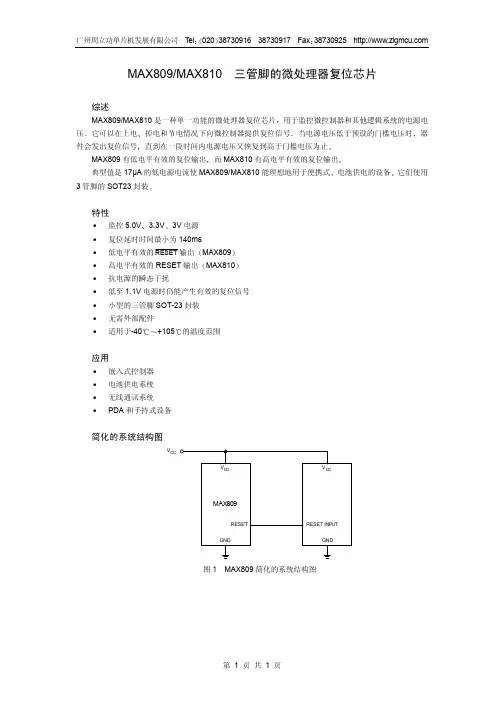
封装MAX809MAX809概述是一款应用于数字系统供电电源电压监控的电压检测芯片,可在工业级标准温度范围内工作。
产生一个复位信号,当系统电源电压降低到设定值时复位信号变低,当系统电源电压恢复到设定值之后芯片会在至少140ms 的延迟时间之后将复位信号置高。
系列产品可以提供任意客户需要的设定检测电压值。
目前我们会提供7个针对5.0V ,3.3V ,3.0V 和2.5V 四类电源电压的标准工业用电压监测值。
提供推挽结构的输出级,当待监测电压高于设定电压值时复位输出高电平。
快速的电源瞬态的抖动和毛刺会被本芯片滤除而不会导致误动作,同时即便供电电压低至1.0V 也能够保证正常的输出逻辑和各性能指标。
提供紧凑的3脚封装形式SOT-23特性◆可工作于工业级温度范围内: -40℃ to +85℃ ◆可低至1V 正常工作 ◆电源毛刺干扰屏蔽功能 ◆提供SOT-23 ◆符合无铅和 RoHS 要求应用范围◆电脑,服务器,笔记本,调制解调器 ◆无线交换机 ◆嵌入式系统 ◆家电,电表◆PDA 和手持设备采用SOT-23典型应用PowerMAX809MAX809MAX809MAX809打标说明及管脚分布SOT-23GNDRESET管脚描述MAX809R MAX809S MAX809T 型号 最高输入电压(V)复位电压(V)容差封装形式SOT23 SOT89-35.5 3.08+2% 5.5 2.93 +2%5.52.63+2%丝印AFAAADAA ACAA ■ 型号选择结构框图VDD注: 超过上表所列的“绝对最大额定值”的应用条件有可能会永久性损害芯片。
此处仅指额定极限指标,并不暗示客户可以将本芯片应用在此条件下或者其他任何超过“推荐工作条件”下。
所有超过“绝对最大额定值”的应用都会影响本芯片的可靠性。
电气特性(如无特别说明,环境温度TA=25℃)MAX MAX809使用说明复位信号将给微处理器一个确定的初始状态,将会给出这样一个复位信号,以防止微处理器在电源上电、下电或者掉电的过程中出现代码执行的错误。