阳极氧化铝为模板电化学沉积铜纳米线
- 格式:pdf
- 大小:590.59 KB
- 文档页数:5


实验一、电镀法制备Fe纳米线一、实验目的1.了解阳极氧化铝模板的制备工艺和制备过程。
2.了解金属纳米线的电镀工艺和带电镀过程。
二、实验设备天平、模具,可调直流稳压电源,温度计,电流表,化学试剂等。
三、原理说明1.阳极氧化铝模板简介阳极氧化铝模板(aluminum oxide template,AAO模板)是通过电化学氧化的方法在纯铝表面形成的具有高度规整结构的氧化铝薄膜。
铝在酸性电解液中阳极氧化时,由于电解液对氧化铝的溶解作用,可形成结构独特的多孔型氧化铝薄膜,这种膜的结构示意图如图1所示。
从图中可以看出,多孔氧化铝包括两层,即与铝基相邻的薄而致密的阻挡层和外表厚而疏松的多孔层,多孔层为六角密排的氧化铝晶胞结构,每个晶胞中央包含一个纳米级的微孔。
这些孔大小均匀,与基体表面垂直,彼此之间相互平行,可作为合成纳米材料的模板。
图1.多孔阳极氧化铝膜的示意图2.阳极氧化铝模板的制备模具外形如图2所示,底座为耐腐蚀的不锈钢,玻璃管可以方便实验中随时观察。
实验过程中,模具放在装有冰水的恒温槽中实现电解液的零度恒温。
在氧化生成氧化铝模板的过程中,流过铝片的电能将转化为热能,从而产生大量的热量,这些热量会导致整个电解槽温度的上升,从而导致电流的增大产生更多的热量;为了维持氧化过程的稳定,我们必须尽量保持整个电解槽温度恒定。
制备氧化铝模板时,当所加电压小时,阳极氧化的速度非常缓慢,模板形成的同时也被酸溶液慢慢腐蚀,难于得到厚的模板;而电压过高又会导致模板的击穿导致实验的失败。
为了得到孔径适中的模板,需要选择合适的电解液;为了提高模板的制备速度,需要选择合适的电压。
实验中所用电解液和电解条件如表1所示。
所用铝片厚度为120 μm,纯度为99.99%,并且已经经过了500 ℃、5小时空气气氛退火处理。
图3.制备氧化铝的模具(左)和实验装置(右)3.电化学沉积法制备金属纳米线电化学沉积就是通常的电镀。
电镀对镀层质量要求较高,因此对镀液的成分要加以控制,有着严格的工艺配方;为了得到光洁、牢固的镀层,还必须对电镀的基底进行除锈、除油处理;电镀电压也要严格加以控制。

铜纳米线的制备铜纳米线是指直径在纳米级别的铜材料,具有良好的电导率和机械性能。
制备铜纳米线的方法有多种,下面将介绍其中的几种常见方法。
一、电化学沉积法电化学沉积法是一种较为常见的制备铜纳米线的方法。
该方法通过在电极表面进行电沉积,实现铜纳米线的生长。
首先,需要准备好电解液,其中含有铜离子。
然后,将电极浸入电解液中,通过施加电压和电流,使铜离子在电极表面还原成铜原子,从而形成铜纳米线。
二、溶剂热法溶剂热法是利用有机溶剂的热溶解性质来制备铜纳米线的方法。
通过在有机溶剂中加入含有铜离子的溶液,并在一定的温度和时间条件下进行加热,利用有机溶剂的热溶解性质,使铜离子还原成铜原子,从而形成铜纳米线。
三、电子束蒸发法电子束蒸发法是一种物理方法,通过电子束照射来制备铜纳米线。
首先,需要将铜材料置于真空腔室中,然后利用电子枪发射出高速电子束,照射到铜材料上。
在电子束的作用下,铜材料表面的原子逐渐蒸发,然后重新沉积在基底上,形成铜纳米线。
四、模板法模板法是一种利用模板的方法来制备铜纳米线。
首先,需要选择一个具有孔隙结构的模板材料,如聚合物膜、氧化铝膜等。
然后,在模板孔隙中沉积铜离子或铜原子,通过化学还原或电化学方法,使其还原成铜纳米线。
最后,将模板材料从铜纳米线中去除,得到单独的铜纳米线。
五、气相沉积法气相沉积法是一种利用气体中的铜原子来制备铜纳米线的方法。
首先,需要将含有铜原子的气体通入反应室中,然后通过控制反应室的温度和压力等条件,使铜原子沉积在基底上,形成铜纳米线。
六、热分解法热分解法是一种利用高温条件下的化学反应来制备铜纳米线的方法。
通过在高温条件下,将含有铜离子的化合物进行热分解,使其还原成铜原子,并在基底上形成铜纳米线。
总结起来,制备铜纳米线的方法有电化学沉积法、溶剂热法、电子束蒸发法、模板法、气相沉积法和热分解法等。
每种方法都有其独特的优势和适用范围,可以根据具体需求选择合适的方法进行制备。
随着纳米技术的不断发展,铜纳米线的制备技术也将不断完善,为其在电子、光电子等领域的应用提供更好的支持。

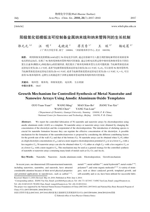
In recent years,one dimensional (1D)nanostructured materials,including nanowires,nanotubes,and nanorods,have attracted considerable attention because of their novel physical properties and potential applications in nanodevices,such as carbon [1-2],metals [3-5],metal sulfides [6-7],metal hydroxide [8],metal oxides [9-10],polymers [11],and some organic molecules [12-13].A variety of strate ⁃gies,such as direct catalyzed growth,templated growth,and self ⁃assembly and so on,have been utilized for successful fabri ⁃阳极氧化铝模板法可控制备金属纳米线和纳米管阵列的生长机制郭元元1,2汪明2毛晓波2蒋月秀1,*王琛2,*杨延莲2,*(1广西大学化学系,南宁530004;2国家纳米科学中心,北京100190)摘要:利用阳极氧化铝模板(AAO)进行Ni 的电化学沉积,通过在溶液中引入螯合剂控制电解质的有效浓度和电沉积的过电位,实现了Ni 纳米线和纳米管阵列的可控制备.通过分析电沉积过程中纳米线和纳米管在不同位置生长速率(侧壁(V w )和底端(V b ))的控制因素,我们提出了纳米线和纳米管生长的可能机制.当电解质浓度高而还原电位更负(如-1.5V)时,或者当电解质浓度低而还原电位较负(如-0.5V)时,V w >V b ,可以获得Ni 纳米管阵列;当电解质浓度高而还原电位较负(如-0.5V)时,或者当电解质浓度低而还原电位更负(如-1.5V)时,V w ≈V b ,可以获得Ni 纳米线阵列.这种生长机制适用于多种金属纳米管或者纳米线阵列的可控制备.关键词:纳米管;纳米线;阳极氧化铝;电沉积;生长机制中图分类号:O647Growth Mechanism for Controlled Synthesis of Metal Nanotube andNanowire Arrays Using Anodic Aluminum Oxide TemplatesGUO Yuan ⁃Yuan 1,2WANG Ming 2MAO Xiao ⁃Bo 2JIANG Yue ⁃Xiu 1,*WANG Chen 2,*YANG Yan ⁃Lian 2,*(1Department of Chemistry,Guangxi University,Nanning 530004,P.R.China ;2National Center for Nanoscience and Technology,Beijing 100190,P.R.China )Abstract :We report the controlled fabrication of Ni nanotube and nanowire arrays by electrodeposition using anodic aluminum oxide (AAO)as a template.Ni nanotube arrays or nanowire arrays were obtained by changing the concentration of the electrolyte and the overpotential of the electrodeposition.The introduction of chelating species is crucial for nanotube formation because they can regulate the effective concentration of the electrolyte.A possible mechanism for the formation of the nanotubes/nanowires is proposed by considering the different contributing factors for the growth rate of the wall (V w )and that of the bottom (V b ).Ni nanotube arrays can be obtained when V w >V b either at a high electrolyte concentrations (C Ni 2+)and at a more negative electrodeposition potential (U ed )or at a lower C Ni 2+with a less negative U ed .Ni nanowire arrays can also be obtained when V w ≈V b either at a high C Ni 2+with a less negative U ed or at a lower C Ni 2+with a more negative U ed .This mechanism may be used as a general strategy for the controlled synthesis of nanotube or nanowire arrays containing many kinds of metals such as Cu,Co,and Au etc.Key Words :Nanotube;Nanowire;Anodic aluminum oxide;Electrodeposition;Growth mechanism[Article]物理化学学报(Wuli Huaxue Xuebao )Acta Phys.鄄Chim.Sin .,2010,26(7):2037-2043July Received:March 15,2010;Revised:May 24,2010;Published on Web:June 4,2010.∗Corresponding authors.JIANG Yue ⁃Xiu,Email:jyx63826@;Tel:+86⁃771⁃3273937.YANG Yan ⁃Lian,Email:yangyl@;Tel:+86⁃10⁃82545559.WANG Chen,Email:wangch@;Tel:+86⁃10⁃82545561.The project was supported by the National Natural Science Foundation of China (20873033,20973043)and National Key Basic Research Program of China (973)(2007CB936800,2006CB932100).国家自然科学基金(20873033,20973043)和国家重点基础研究发展规划项目(973)(2007CB936800,2006CB932100)资助ⒸEditorial office of Acta Physico ⁃Chimica Sinica2037Acta Phys.鄄Chim.Sin.,2010Vol.26Table 1Electrodeposition conditions for preparing Ni nanotubes and nanowirescation of 1D nanomaterials [14-16].Among these methods,the tem ⁃plated synthesis of 1D nanomaterials using the anodic aluminum oxide (AAO)is an effective venue for fabricating nanotubes and nanowires of metals,metal oxides,fullerenes,organic molecul ⁃es [17-19],as well as metallic 1D nanomaterials [20-22].The well ⁃defined length and diameter of the AAO channels facilitate controlled fabrication of 1D nanostructures.Chemical replacement [23],chem ⁃ical infiltration [24],chemical vapor deposition (CVD)[25],and elec ⁃trochemical deposition [26-27]have been utilized for preparation of 1D nanomaterials within the porous alumina template.Among these techniques,electrodeposition method was widely used for preparing metallic and semiconducting nanowires,such as Ni,Cu,Au,Ag,bimetallic nanowire junctions for magnetic,catalytic applications [28-29].It could be noted that metal nanotubes are con ⁃sidered very promising for high performance catalysts [30-31],highly sensitive gas sensors [31-33],and up ⁃conversion non ⁃linear optics [34],etc.Thus,many efforts have been put into the controlled syn ⁃thesis of metal nanotubes.As a general approach to fabricate well ⁃defined metal nanotubes,the inner surfaces of the AAO channels are usually chemically modified with suitable func ⁃tional groups ⁃molecular anchors [35-36],so that the electrodeposited metal atoms can bind to the nanopore walls to form nanotubes.A number of metallic nanotubes have been successfully synthe ⁃sized by this method,while the unavoidable organic impurities introduced from the chemical modification process limited its applications [37-38].Metal nanotubes can also be obtained by con ⁃trolling the thickness of the electrode film for preventing the pores from being blocked [39-40]and followed by electrodeposition of the metals [41].The fabrication via multi ⁃step template replica ⁃tion and electrodeposition approach was also reported to get metal nanotube array [42].Fundamentally the growth of metal nanotubes and nanowires is governed by the electrochemical deposition process and the concentration diffusion of the metal ions.The understanding of the growth mechanism would benefit the controlled fabrication of desired metal nanostructures for specific applications.Some reports have attributed the nanotube growth to the well ⁃known tip effect [43-44].Recently,Yoo et al .[20]proposed the bottom ⁃up and the wall ⁃up growth modes to describe the metal nanotube for ⁃mation,and also reported the preparation of Pt and Pd nanotubes by a wall ⁃up growth mechanism at high current density.Cao et al .[45]also reported the controlled preparation of metal (Fe,Co,Ni)nanotube arrays and proposed a mechanism of competitive growth rates along two directions:parallel to and perpendicularto the current direction.The mechanisms proposed by Yoo [20]and Cao [45]et al .can be considered principally the same.In addi ⁃tion,Chowdhury et al .[46]put forward the mechanism related to overpotential increase by gas evolution for the central portion shielding and thus the promotion of the reaction at the sides of the porous mon to these studies is that the nano ⁃tube formation is dependent on the different growth rates of the metal along the wall surface (V w )and from the central bottom of the nanochannels (V b ),while systematic studies are still needed to fully understand the growth mechanisms which are critical for controlled growth of nanowires and nanotubes.In this work,we examined the controllable synthesis of Ni nanowires and nano ⁃tubes by electrodeposition method using AAO as template.Based on the systematic studies,mechanisms for the nanowire and nanotube growth were proposed.1Experimental1.1Templated electrodepositionThe AAO templates used in our experiments were purchased from Whatman Company (Anodisc 47,200nm in nominal pore diameter and 60μm in thickness).The electrodeposition was carried out with the constant potential mode in a conventional three ⁃electrode electrochemical cell.Before the electrodeposi ⁃tion,Au film was first deposited as an electrode on one side of the AAO membrane using a vacuum evaporation apparatus and a small portion of the inside channels were filled to shape a bowl ⁃like structure [4,43].AAO template coated by Au layer,a piece of platinum plate (ca 1.0cm 2),and a calomel electrode were used as the working,counter,and reference electrodes,respectively.All the electrodeposition experiments were performed at room temperature and the deposition time was kept constant at 1000s.The electrochemical deposition was conducted in aqueous so ⁃lutions containing NiSO 4·6H 2O (AR),ethylenediaminetetraace ⁃tic acid (EDTA,AR),NaOH (AR),and K 2HPO 4(AR).The con ⁃centration of EDTA was two times higher than that of the Ni 2+ions.The concentration of K 2HPO 4was kept constant at 20g ·L -1and the pH values were adjusted by NaOH to 11for the solu ⁃tions with EDTA.All the solutions were prepared with ultrapure Milli Q water (resistivity ≥18M Ω·cm).The electrodeposition was performed at room temperature and the detailed electrode ⁃position conditions are shown in Table 1.1.2Characterization of Ni nanowires or nanotubes After electrodeposition,the AAO templates were removed by immersion in 2mol ·L -1NaOH solutions at 25℃for 2h.Then,*For samples 3,4,7,and 8,nanotubes or nanowires in the brackets are the resulted nanostructures with less probability coexisting with the major nanostructures listedbefore the brackets.U ed :potentialSample No.Result U ed /V Electrolyte compositionU ed /V Result Sample No.1nanotubes -1.50.05mol ·L -1NiSO 4,0.1mol ·L -1EDTA,20g ·L -1K 2HPO 4,pH=11-0.5nanowires 52nanotubes -1.50.01mol·L -1NiSO 4,0.02mol ·L -1EDTA,20g ·L -1K 2HPO 4,pH=11-0.5nanowires 63478nanowires(nanotubes)*nanowires (nanotubes)*-1.5-1.50.005mol ·L -1NiSO 4,0.01mol ·L -1EDTA,20g ·L -1K 2HPO 4,pH=110.001mol ·L -1NiSO 4,0.002mol ·L -1EDTA,20g ·L -1K 2HPO 4,pH=11-0.5nanowires (nanotubes)*nanotubes (nanotubes)*-0.52038No.7GUO Yuan ⁃Yuan et al .:Growth Mechanism for Controlled Synthesis of Metal Nanotube and Nanowire Arraysthe as ⁃prepared samples were thoroughly rinsed with distilledwater and subsequently dried in air.Scanning electron micro ⁃scopic (SEM)characterizations of the products were performed on a Hitachi S ⁃3400N SEM apparatus.For transmission electron microscopic (TEM)characterizations,the samples were subjected to ultrasonic treatment in ultrapure water for 1min,then a drop of suspension was dipped on the carbon ⁃coated copper grid.All TEM characterizations were performed on an FEI TEM (Tecnai G220)at an accelerating voltage of 120kV.X ⁃ray photoelec ⁃tron spectroscopic (XPS)measurements were conducted on an XPS spectrometer (VG Scientific ESCALab 220i ⁃XL)operated at 300W in vacuum (3×10⁻⁷Pa)with a monochromatic Al K 琢radi ⁃ation.The binding energies were corrected for charging by ad ⁃ventitious carbon (C 1s )at 284.8eV.Curve fitting of the XPS spectra was performed by using XPS PEAK software.2Results and discussion2.1Impact of chelating agent EDTAElectrodeposition of Ni was conducted with the aid of the AAO template for the preparation of nanowire or nanotube ar ⁃rays.All the samples were etched using NaOH solution for 2h to remove the AAO membrane,thus the nanowires or nanotubes can be exposed from the template.The Ni nanowires can be ob ⁃tained in the solution (the concentration of Ni ions,C Ni 2+=0.01mol ·L -1)without addition of EDTA at electrodeposition poten ⁃tial U ed =-1.5V.SEM image in Fig.1(a)shows highly ordered Ni nanowire arrays with uniform structures in large area.The aver ⁃age diameter of the Ni nanowires is about 200nm which resem ⁃bles the pore diameter of the AAO template (200nm).Upon the introduction of EDTA,nanotube arrays could be obtained with the same C Ni 2+(0.01mol ·L -1)and the same U ed (-1.5V).SEM im ⁃age in Fig.1(b)reveals the typical morphology of the highly or ⁃dered Ni nanotube arrays with clear open ends.The outer diam ⁃eters of the nanotubes were around 200nm (nearly the same as the pore diameter of the AAO template)and the inner diameters were around 140-160nm.In other words,the thickness of nan ⁃otube walls was about 20-30nm.The length of the nanotubes and nanowires could reach about 20μm in 1000s.The conversion of the nanowire to nanotube morphology with the introduction of the EDTA into the solution demonstrated the impact of the coordination ion on the eletrodeposition mecha ⁃nisms.The growth of nanowires and nanotubes can be viewed as a balance between two dominated growth rates,V w and V b .The bottom ⁃up and the wall ⁃up growth modes proposed by Yoo et al .[20],and the current ⁃directed tubular growth (CDTG)mech ⁃anisms proposed by Cao et al .[45],have revealed the relationship between the morphologies of the 1D nanomaterials and the cur ⁃rent densities at different locations.However,the underlying mechanism for the relationship of the current densities and the growth rates is still need to be clarified.In the reduction process of nickel ions,nanotubes can be obtained if V w >V b .It should be noted that both V w and V b could be affected by the introduction of the chelating agent EDTA,and the well ⁃known tip growth ef ⁃fect should be also taken into account.The electrochemical de ⁃position process of Ni with EDTA can be divided into three steps as following.a)The coordination of Ni 2+with EDTA.There are seven forms for EDTA in solution (H 6Y 2+,H 5Y +,H 4Y,H 3Y -,H 2Y 2-,HY 3-,Y 4-)and their populations are dependent on the solution acidity.The complex NiY 2-is the compound with the highest population when pH>10.The chelation and the dissociation balance of the complex can be described as below.Ni 2++Y 4-⇌NiY 2-b)The diffusion of NiY 2-and Ni 2+ions to the surface of the electrode.When the Ni 2+was depleted near the working elec ⁃trode,it will be supplied by the dissociation of NiY 2-.The con ⁃centration of Ni 2+was limited in the range of 10-16mol ·L -1,be ⁃cause the stability constant of the complex was 1018and the con ⁃centration of Y 4-ions was kept in the range of 10-2mol ·L -1.c)At last,Ni 2+receives electrons on the surface of the cathode and forms nanotubes or nanowires.As mentioned above,Au film deposited as a working electrode at the bottom of the AAO membrane with bowl ⁃shaped structures [4,43].Because of the tip ef ⁃fect,the edge tips of the initial bowl ⁃shaped Au electrode give rise to higher electric field,which is electrochemically more ac ⁃tive than the smooth surface.Meanwhile,the surface energy of the inner walls of the nanochannels [48]also facilitates the bottom edge of the nanochannels to be a preferential site for the deposi ⁃tion of metal ions.Considering that the effective growth rate is correlated to the effective Ni 2+concentration,the addition of EDTA would result in decreased reduction rate of NiY 2-com ⁃pared with that of the Ni 2+hydrate.Both V w and V b were greatly reduced by the chelating agent.At this slower reduction rate,the tip effect of the electric field would render the predominance of the higher deposition rate of V w (V w >V b )and finally give rise to the formation of metal nanotubes.On the contrary,both of the growth rates (V w and V b )are very fast in the solution without EDTA,so the tip effect could be ignored (V w ≈V b ),thus the nanowires can be obtained.2.2Impact of electrodeposition potential andelectrolyte concentrationThe electrodeposition potential is a key factor for the forma ⁃tion of metal nanotubes and nanowires.When other conditions are constant,more negative U ed (higher than the potential for gas evolution)would lead to the higher current density which isFig.1SEM images of Ni nanowire and nanotube arrayswithout and with EDTA(a)top view of the Ni nanowires deposited from the solution with C NiSO 4=0.01mol ·L -1at U ed =-1.5V;(b)top view of the Ni nanotubes deposited from thesolution with C NiSO 4=0.01mol ·L -1,C EDTA =0.02mol ·L -1,C K 2HPO 4=20g ·L -1atU ed =-1.5V (sample2)2039Acta Phys.鄄Chim.Sin.,2010Vol.26keenly related to the growth rates,V b and V w ,thus the final mor ⁃phology of the 1D metallic nanostructures.Meantime,U ed also influences the electromigration rate of the NiY 2-,which has the opposite direction to the concentration diffusion in the solution.In order to further understand the growth mechanism for the formation of metal nanotubes and nanowires,systematic studies were performed under different conditions listed in Table 1.At a higher NiY 2-ion concentration (sample 1),Ni nanotubes with thin wall could be gained at more negative U ed =-1.5V.When the concentration of NiY 2-decreases gradually (samples 1-4),at U ed =-1.5V,the SEM images in Fig.2(a,d,e)clearly illustrate the evolution of the 1D nanomaterials from well ⁃aligned nanotubes in sample 1,to coexistence of nanotubes and nanowires (mainly nanotubes)in sample 3and finally to coexistence of nanowires and nanotubes (mainly nanowires)in sample 4.In addition,the gradual increase of the nanowire proportions is also accompa ⁃nied by the gradual increase of the nanotube wall thickness.The TEM image in Fig.2(b)clearly shows the typical hollow structure of the nanotubes (sample 2).The selected ⁃area electron diffrac ⁃tion pattern in Fig.2(c)was acquired from a 200nm diameter Ni nanotubes in sample 2.The continuous bright rings indicate the polycrystalline structure with face ⁃centered cubic Ni metals,in which the lattice parameters 0.202,0.175,and 0.124nm corre ⁃spond to the facets (111),(200),and (220),repectively.Fig.3(a)presents the XPS spectrum of Ni nanotubes,which are fabricat ⁃ed under the condition of sample 2.The binding energy of Ni (metal)is 853.1eV which is consistent with the reported value in the reference [49].Three Ni 2p 3/2peaks (Ni,Ni (satellite),and NiO)reveal that the Ni nanotubes were mainly composed of metallic Ni.The existence of NiO is unavoidable due to the oxidation of the surface of Ni nanotubes exposed to the air.Interestingly,Ni nanowires could be obtained at less negative potential (U ed =-0.5V,Table 1)in the solutions with higher NiY 2-concentrations (samples 5and 6).Ni nanotubes would gradually appear and coexist with Ni nanowires in the solution with medium NiY 2-concentration (sample 7).When the concentration of NiY 2-was decreased to 0.001mol ·L -1(sample 8),Ni nanotubes became the dominant 1D nanostructures.The SEM images in Fig.4(a,c,d)(samples 5,6,8correspondingly)present the evolution from Ni nanowires to nanotubes in view of the end features of the 1D nanostructures from flat ends (sample 5),bowl ⁃shaped ends (sam ⁃ple 6),to open ends (sample 8).The solid structure of the nanowire (sample 5)has also been proved by TEM characterizations (Fig.4(b)).The XPS spectrum for Ni nanowires in sample 5(Fig.3(b))shows that the metallic Ni is the main component with the appearance of NiO ascribed to the oxidation of Ni in the air,which is similar to the nanotubes in sample 2(Fig.3(a)).The evolution from nanotubes to nanowires at more negative U ed and from nanowires to nanotubes at less negative U ed indicated the coef ⁃fect of the electrolyte concentrations and the electrodeposition potentials.2.3Proposed mechanism for electrodeposition ofnanotubes or nanowiresFrom the systematic studies above,Fig.5(a,b)can be proposedFig.2SEM and TEM images of Ni nanowire and nanotube arrays deposited at U ed =-1.5V(a)top view of the Ni nanotubes deposited from the solution with C NiSO 4=0.05mol·L -1,C EDTA =0.1mol ·L -1,C K 2HPO 4=20g ·L -1(sample 1),(b)typical TEM image of a piece of Ni nanotubes deposited from the solution with C NiSO 4=0.01mol ·L -1,C EDTA =0.02mol ·L -1,C K 2HPO 4=20g ·L -1(sample 2),(c)selected area electron diffraction pattern acquiredfrom a Ni nanotube with 200nm diameter (sample 2),(d)top view of the Ni nanotubes (nanowires)deposited from the solution with C NiSO 4=0.005mol ·L -1,C EDTA =0.01mol ·L -1,C K 2HPO 4=20g ·L -1(sample 3),(e)top view of the Ni nanowires (nanotubes)deposited from the solution with C NiSO 4=0.001mol ·L -1,C EDTA =0.002mol ·L -1,C K 2HPO 4=20g ·L -1(sample4)2040No.7GUO Yuan ⁃Yuan et al .:Growth Mechanism for Controlled Synthesis of Metal Nanotube and Nanowire Arraysto schematically illustrate the electrodeposition processes in theelectrolytes with higher NiY 2-ion concentration at U ed =-1.5V and U ed =-0.5V.The electromigration of NiY 2-ions can be ne ⁃glected when the NiY 2-ion concentration near the working elec ⁃trode is high enough.The faster reduction rate at more negative U ed would enhance the tip effect leading to the nanotube forma ⁃tion due to V w >V b .The underlying mechanism may be proposed that the bottom and the wall will grow together at beginning,while the faster growth rate will deplete the NiY 2-ions in the nanochannels.The shorter distance from the bulk solution to the nanochannels would lead to the faster diffusion of NiY 2-ions to the far front ends of the deposited Ni,which renders the domi ⁃nant tip effect for nanotube growth.When it comes to the solution with the same higher concentration of the NiY 2-,while at less negative U ed (-0.5V,Fig.5(b)),the reduction rate is much slow ⁃er than that at -1.5V.The diffusion rate of NiY 2-ions from the bulk solution to the nanochannels is high enough to overcome the edge ⁃predominance,which leads to the similar lower growth rates of the wall surface and the bottom (V w 抑V b ).Then the bot ⁃tom and the wall would grow together and finally result in the formation of nanowire arrays (Fig.5(b)).When the concentration of the NiY 2-ions is decreased to very low level in Fig.5(c,d)(such as 0.001mol ·L -1),the fabricated nanostructures indicated the opposite trends for nanotube and nanowire compared with those at higher NiY 2-ion concentra ⁃tions,that is nanowires at -1.5V and nanotubes at -0.5V.BesidesFig.3XPS spectra of Ni nanotubes (sample 2)and nanowires (sample 5)(a)Ni 2p 3/2peak in the XPS spectrum of Ni nanotubes deposited from the solution with C NiSO 4=0.01mol·L -1,C EDTA =0.02mol ·L -1,C K 2HPO 4=20g ·L -1at U ed =-1.5V (sample 2),(b)Ni 2p 3/2peak in the XPS spectrum of Ni nanowires deposited from the solution with C NiSO 4=0.05mol ·L -1,C EDTA =0.1mol ·L -1,C K 2HPO 4=20g ·L -1at U ed =-0.5V (sample 5).Curve fitting of the XPS spectra was performed by using XPS PEAK software.The corresponding peaks obtained from the curve fitting are asigned as Ni,Ni (satellite),and NiO,respectively.Full survey XPS spectra for the Ni nanotubes (sample 2)and Ni nanowires (sample 5)can be found in Supporting Information (Fig.S1),which are available free of charge via the internet at.Fig.4SEM and TEM images of Ni nanowire and nanotube arrays deposited at U ed =-0.5V(a)top view of the Ni nanowires deposited from the solution with C NiSO 4=0.05mol ·L -1,C EDTA =0.1mol ·L -1,C K 2HPO 4=20g ·L -1(sample 5),(b)typical TEM image of a piece ofNi nanowire in sample 5,(c)top view of the Ni nanowires deposited from the solution with C NiSO 4=0.01mol ·L -1,C EDTA =0.02mol ·L -1,C K 2HPO 4=20g ·L -1(sample 6),(d)top view of the Ni nanotubes (nanowires)deposited from the solution with C NiSO 4=0.001mol ·L -1,C EDTA =0.002mol ·L -1,C K 2HPO 4=20g ·L -1(sample8)2041Acta Phys.鄄Chim.Sin.,2010Vol.26the U ed mentioned above,the effect of electromigration on the growth rates,V w and V b ,should also be taken into account at lower diffusion rate.The electromigration of NiY 2-ions to the counter electrode and concentration diffusion to the work elec ⁃trodes can both increase the overpotential for the electrochemi ⁃cal deposition.The increased overpotential could lead to the de ⁃crease of the V w and the V b .The reduction rate of the Ni 2+is rela ⁃tively faster at more negative U ed (Fig.5(c),such as -1.5V),while the lower diffusion rate of the NiY 2-ions would largely reduce the deposition rate.So the similar growth rate of the wall and the bottom V w 抑V b would be obtained for the nanowire formation.We believe that the similar growth rates at middle level in cases of Fig.5(b,c)give rise to the similar results,which is originated from the balance between the potential effect and the concentra ⁃tion effect.At less negative U ed (-0.5V),the reduction rate of Ni 2+should be very low at lower concentration of the NiY 2-ions.The less influence of the NiY 2-electromigration and the very low re ⁃duction rate make the diffusion of the NiY 2-ions sufficient enough.The Ni 2+ions on the edge can be supplemented in time and adsorbed on the edge preferentially.As the result,the V w is relatively higher than the V b ,which leads to the final nanotube formation.Based on the above mentioned mechanism,Cu nanotube and nanowire arrays have also been fabricated at higher electrolyte concentration with more negative U ed (Fig.S2,which is available free of charge via the internet at ).The nanowires can be obtained without the introduction of the chelating agent EDTA,while the nanotube arrays can be obtained with EDTA.The common mechanism for 1D nanostructure growth of Ni and Cu indicates that it could be a general strategy for growth of metal nanotubes and nanowires.The controlled preparation of Au (Fig.S3)and Co (Fig.S4)(which are availableFig.5Schematic diagrams of the growth processes of Ni nanotubes and nanowires at different electrodeposition conditions(a)and (b)are schematic diagrams of the growth processes of nanotubes at U ed =-1.5V and nanowires at U ed =-0.5V in the electrolytes with higher NiY 2-concentrations,respectively,(c)and (d)are schematic diagrams of the growth processes of nanowires at U ed =-1.5V and nanotubes at U ed =-0.5V in the electrolytes with lower NiY 2-concentrations,respectively.The dashed arrows represent the electromigration direction of NiY 2-and their lengths show the different electromigration rates.The solidarrows represent the concentration diffusion direction of NiY 2-.2042No.7GUO Yuan⁃Yuan et al.:Growth Mechanism for Controlled Synthesis of Metal Nanotube and Nanowire Arraysfree of charge via the internet at ) nanotube arrays at the similar electrodeposition conditions with the chelating agent(EDTA)confirms the possible application of this mechanism in fabrication of other1D metal nanomaterials. 3ConclusionsIn summary,controlled synthesis of Ni nanotube and nanowire arrays can be obtained by electrodeposition using AAO template. Both nanotubes and nanowires can be readily achieved by vary⁃ing the electrodeposition potential and the concentration of NiY2-.The detailed growth mechanism for metal nanotubes and nanowires was proposed based on systematic studies.The cru⁃cial contributing factors of the chelating agent,the electrodepo⁃sition potential,the concentration of the NiY2-,and the electro⁃migration were all taken into account for clarification of the growth process.This method could be applicable to fabrication of other metal nanotubes and nanowires,which has high pote⁃tials for applications in nanocatalyses,chemical sensors,and nanoscale electronic and magnetic devices. Acknowledgment:The authors would like to thank Dr.ZHONG Liang⁃Shu and Dr.LIANG Han⁃Pu at the Institute of Chemistry,Chi⁃nese Academy of Sciences for helpful discussion in electrodeposition experiments.References1Iijima,S.Nature,1991,354:562Li,Y.L.;Kinloch,A.;Windle,A.H.Science,2004,304:2763Wirtz,M.;Martin,C.R.Adv.Mater.,2003,15:4554Zhang,X.Y.;Zhang,L.D.;Lei,Y.;Zhao,L.X.;Mao,Y.Q.J.Mater.Chem.,2001,11:17325Hong,B.H.;Bae,S.C.;Lee,C.W.;Jeong,S.;Kim,K.S.Science, 2001,294:3486Chen,J.;Tao,Z.;Li,S.Angew.Chem.Int.Edit.,2003,42:2147 7Xu,D.S.;Xu,Y.J.;Chen,D.P.;Guo,G.L.;Gui,L.L.;Tang,Y.Q.Chem.Phys.Lett.,2000,325:3408Zhang,W.;Wen,X.;Yang,S.;Berta,Y.;Wang,Z.L.Adv.Mater., 2003,15:8229Yan,C.;Xue,D.Adv.Mater.,2008,20:105510Huang,B.H.;Shen,P.Y.;Chen,S.Y.Nanoscale Res.Lett.,2009, 4:50311Xiao,R.;Cho II,S.;Liu,R.;Lee,S.B.J.Am.Chem.Soc.,2007, 129:448312Lu,Q.;Gao,F.;Komarneni,S.;Mallouk,T.E.J.Am.Chem.Soc., 2004,126:865013Matsumoto,F.;Nishio,K.;Masuda,H.Adv.Mater.,2004,16: 210514Korgel,B.A.;Fitzmaurice,D.Adv.Mater.,1998,10:66115Wang,M.H.;Li,Y.J.;Xie,Z.X.;Liu,C.;Yeung,E.S.Mater.Chem.Phys.,2010,119:15316Gao,P.;Cai,Y.G.ACS Nano,2009,3:347517Xiao,Z.L.;Han,C.Y.;Welp,U.;Wang,H.H.;Kwok,W.K.;Hiller,J.M.;Cook,R.E.;Miller,D.J.;Crabtree,G.W.Nano Lett.,2002,2:129318Martin,C.R.Science,1994,266:196119Gao,H.;Mu,C.;Wang,F.;Xu,D.S.;Wu,K.;Xie,Y.C.;Liu,S.;Wang,E.G.;Xu,J.;Yu,D.P.J.Appl.Phys.,2003,93:560220Yoo,W.C.;Lee,J.K.Adv.Mater.,2004,16:109721Wang,Y.;Wu,K.J.Am.Chem.Soc.,2005,127:968622Qu,L.T.;Shi,G.Q.;Wu,X.F.;Fan,B.Adv.Mater.,2004,16: 120023Yan,C.;Xue,mun.,2007,9:124724Wang,Y.;Lee,J.Y.;Zeng,H.C.Chem.Mater.,2005,17:3899 25Franklin,N.;Dai,H.Adv.Mater.,2000,12:89026Routkevitch,D.;Bigioni,T.;Moskovits,M.;Xu,J.M.J.Phys.Chem.,1996,100:1403727Kamalakar,M.V.;Raychaudhuri,A.K.Adv.Mater.,2008,20:149 28Wang,H.;Xu,C.W.;Cheng,F.L.;Jiang.S.P.Electrochem.Commun.,2007,9:121229Liang,H.P.;Guo,Y.G.;Hu,J.S.;Zhu,C.F.;Wan,L.J.;Bai,C.L.Inorg.Chem.,2005,44:301330Yang,L.X.;He,D.M.;Cai,Q.Y.J.Phys.Chem.C,2007,111: 821431Han,C.H.;Hong,D.W.;Kima,I.J.;Gwak,J.;Han,S.D.;Singh, K.C.Sens.Actuators B,2007,128:32032Andzelm,J.;Govind,N.;Maiti,A.Chem.Phys.Lett.,2006,421:58 33Sadrzadeh,A.;Farajian,A.A.;Yakobson,B.I.Appl.Phys.Lett., 2008,92:02210334Schider,G.;Krenn,J.R.;Gotschy,W.;Lamprecht,B.;Ditlbacher,H.;Leitner,A.;Aussenegg,F.R.J.Appl.Phys.,2001,90:3825 35Lee,W.;Scholz,R.;Lee,N.K.W.;Scholz,R.;Nielsch,K.;Gosele, U.Angew.Chem.Int.Edit.,2005,44:605036Bao,J.;Tie,C.;Xu,Z.;Zhou,Q.;Shen,D.;Ma,Q.Adv.Mater., 2001,13:163137Levina,L.;Sukhovatkin,V.;Musikhin,S.;Cauchi,S.;Nisman,R.;Bazett⁃Jones,D.P.;Sargent,E.H.Adv.Mater.,2005,17:1854 38Nanda,K.K.;Kruis,F.E.;Fissan,H.Nano Lett.,2001,1:60539Li,L.;Pan,S.S.;Dou,X.C.;Zhu,Y.G.;Huang,X.H.;Yang,Y.W.;Li,G.H.;Zhang,L.D.J.Phys.Chem.C,2007,111:7288 40Zhang,X.Y.;Wang,H.T.;Bourgeois,L.;Pan,R.J.;Zhao,D.Y.;Webley,P.A.J.Mater.Chem.,2008,18:46341Fu,J.;Cherevko,S.;Chung,mun.,2008, 10:51442Mu,C.;Yu,Y.X.;Wang,R.M.;Wu,K.;Xu,D.S.;Guo,G.L.Adv.Mater.,2004,16:155043Huang,C.W.;Hao,Y.W.Nanotechnology,2009,20:445607 44Liu,L.F.;Zhou,W.Y.;Xie,S.S.;Song,L.;Luo,S.D.;Liu,D.F.;Shen,J.;Zhang,Z.X.;Xiang,Y.J.;Ma,W.J.;Ren,Y.;Wang,C.Y.;Wang,G.J.Phys.Chem.C,2008,112:225645Cao,H.Q.;Wang,L.D.;Qiu,Y.;Wu,Q.Z.;Wang,G.Z.;Zhang, L.;Liu,X.W.ChemPhysChem,2006,7:150046Chowdhury,T.;Casey,D.P.;mun., 2009,11:120347Lahav,M.;Sehayek,T.;Vaskevich,A.;Rubinstein,I.Angew.Chem.Int.Edit.,2003,42:557648Liu,F.;Zhao,Z,J.;Qiu,L,M.;Zhao,L,Z.Anal.Test.Technol.Instrum.,2009,15:12043。


阳极氧化铝模板辅助电化学沉积法制备FePt纳米合金的研究的开题报告一、选题背景近年来,具有高磁学性能的纳米合金材料在数据存储、生物医学、磁性催化等领域有着广泛的应用。
FePt纳米合金由于其高矫顽力和高磁各向异性而备受关注,但传统合成方法存在合成温度高、析出不均匀等问题,因此寻找一种简单有效的合成方法成为研究的重点之一。
本研究拟采用阳极氧化铝(AAO)模板辅助电化学沉积法制备FePt纳米合金,通过优化相关工艺参数,获得具有优异磁性能的纳米合金材料。
二、研究意义1. 制备具有优异磁性能的FePt纳米合金,有望应用于数据存储、生物医学、磁性催化等领域。
2. 阳极氧化铝模板辅助电化学沉积法具有简单、经济、高效等优点,可以为纳米合金材料的制备提供一种新的思路和方法。
3. 通过优化相关工艺参数,可以不仅提高FePt纳米合金的制备效率,还能够提高其磁性能,对纳米材料制备的研究有着重要的参考价值。
三、研究内容及方法1. 准备阳极氧化铝模板。
2. 采用电化学沉积法,在阳极氧化铝模板上制备FePt纳米合金。
3. 优化工艺参数,包括沉积时间、电压、电解液浓度等,对制备的FePt纳米合金进行表征。
4. 利用扫描电子显微镜(SEM)、透射电子显微镜(TEM)、X射线衍射(XRD)等技术对样品进行表征,研究其结构和形貌特点。
5. 最后利用磁性测量系统对合成的FePt纳米合金进行磁学性能测量,得出其磁性能参数。
四、研究进度安排1. 6月:搜集文献,准备开题报告。
2. 7月:准备阳极氧化铝模板。
3. 8月:采用电化学沉积法制备FePt纳米合金。
4. 9月:优化工艺参数,对制备的FePt纳米合金进行表征。
5. 10月:利用扫描电子显微镜、透射电子显微镜、X射线衍射等技术对样品进行表征。
6. 11月:进行磁性测量,得出其磁性能参数。
7. 12月:完善论文,撰写毕业论文。
五、预期成果本研究拟通过阳极氧化铝模板辅助电化学沉积法制备FePt纳米合金,对制备工艺进行优化,并从形貌和结构角度分析样品特点,确定其磁性能参数,最终可以得出具有优异磁性能的FePt纳米合金材料。