quartus ii 常见的19个错误、28个警告
- 格式:doc
- 大小:34.00 KB
- 文档页数:6

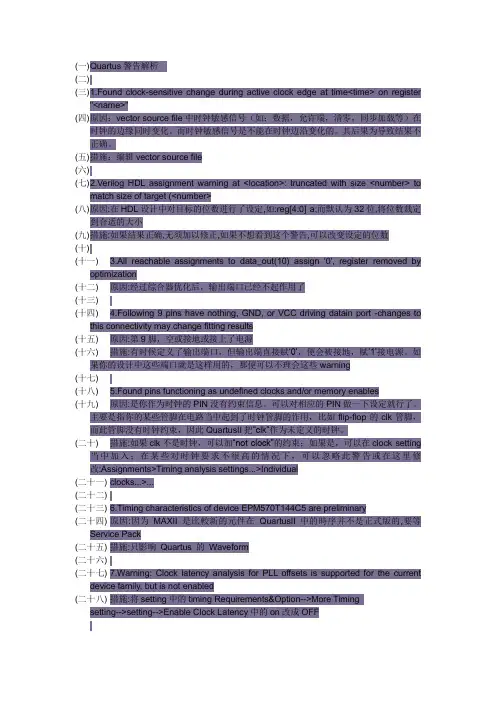
(一) Q uartus警告解析(二)(三) 1.Found clock-sensitive change during active clock edge at time<time> on register"<name>"(四) 原因:vector source file中时钟敏感信号(如:数据,允许端,清零,同步加载等)在时钟的边缘同时变化。
而时钟敏感信号是不能在时钟边沿变化的。
其后果为导致结果不正确。
(五) 措施:编辑vector source file(六)(七) 2.Verilog HDL assignment warning at <location>: truncated with size <number> tomatch size of target (<number>(八) 原因:在HDL设计中对目标的位数进行了设定,如:reg[4:0] a;而默认为32位,将位数裁定到合适的大小(九) 措施:如果结果正确,无须加以修正,如果不想看到这个警告,可以改变设定的位数(十)(十一) 3.All reachable assignments to data_out(10) assign '0', register removed by optimization(十二) 原因:经过综合器优化后,输出端口已经不起作用了(十三)(十四) 4.Following 9 pins have nothing, GND, or VCC driving datain port -changes to this connectivity may change fitting results(十五) 原因:第9脚,空或接地或接上了电源(十六) 措施:有时候定义了输出端口,但输出端直接赋‘0’,便会被接地,赋‘1’接电源。
Quartus II常见编译错误锦集在QuartusII下进行编译和仿真的时候,会出现一堆warning,有的可以忽略,有的却需要注意,虽然按F1可以了解关于该警告的帮助,但有时候帮助解释的仍然不清楚,大家群策群力,把自己知道和了解的一些关于警告的问题都说出来讨论一下,免得后来的人走弯路.下面是我收集整理的一些,有些是自己的经验,有些是网友的,希望能给大家一点帮助。
1.Found clock-sensitive change during active clock edge at time on register""原因:vector source file中时钟敏感信号(如:数据,允许端,清零,同步加载等)在时钟的边缘同时变化。
而时钟敏感信号是不能在时钟边沿变化的。
其后果为导致结果不正确。
措施:编辑vector source file2.Verilog HDL assignment warning at:truncated value with size to match size of target(原因:在HDL设计中对目标的位数进行了设定,如:reg[4:0]a;而默认为32位,将位数裁定到合适的大小措施:如果结果正确,无须加以修正,如果不想看到这个警告,可以改变设定的位数3.All reachable assignments to data_out(10)assign'0',register removed by optimization原因:经过综合器优化后,输出端口已经不起作用了4.Following9pins have nothing,GND,or VCC driving datain port--changes to this connectivity may change fitting results原因:第9脚,空或接地或接上了电源措施:有时候定义了输出端口,但输出端直接赋‘0’,便会被接地,赋‘1’接电源。
在QuartusII下进行编译和仿真的时候,会出现一堆warning,有的可以忽略,有的却需要注意,虽然按F1可以了解关于该警告的帮助,但有时候帮助解释的仍然不清楚,大家群策群力,把自己知道和了解的一些关于警告的问题都说出来讨论一下,免得后来的人走弯路.下面是我收集整理的一些,有些是自己的经验,有些是网友的,希望能给大家一点帮助,如有不对的地方,请指正,如果觉得好,请版主给点威望吧,谢谢1.Found clock-sensitive change during active clock edge at time <time> on register "<name>"原因:vector source file中时钟敏感信号(如:数据,允许端,清零,同步加载等)在时钟的边缘同时变化。
而时钟敏感信号是不能在时钟边沿变化的。
其后果为导致结果不正确。
措施:编辑vector source file2.Verilog HDL assignment warning at <location>: truncated value with size <number> to match size of target (<number>原因:在HDL设计中对目标的位数进行了设定,如:reg[4:0] a;而默认为32位,将位数裁定到合适的大小措施:如果结果正确,无须加以修正,如果不想看到这个警告,可以改变设定的位数3.All reachable assignments to data_out(10) assign '0', register removed by optimization原因:经过综合器优化后,输出端口已经不起作用了4.Following 9 pins have nothing, GND, or VCC driving datain port -- changes to this connectivity may change fitting results原因:第9脚,空或接地或接上了电源措施:有时候定义了输出端口,但输出端直接赋‘0’,便会被接地,赋‘1’接电源。

设计中从硬件到软件,不断有新的问题出现,先将出现的典型问题罗列如下。
1.Maxplus2功能问题:Maxplus2对用于数组描述的RAM及ROM在编译过程中会出错,有可能是M axplus2在语法支持上不太全面。
该用Quarters II运行或用元件例化的方法解决。
例如:subtype word is std_logic_vector(k-1downto0);type memory is array(0to2**w-1)of word;解决:在QuartusП上运行通过。
2.进行仿真实验时,结束时间设为100us时出现的问题:解决:不改动原状态的时间设置。
3.管脚编辑出现的问题:原因是自己改变了原来的管脚编号4.毛刺信号的产生信号在FPGA器件内部通过连线和逻辑单元时,都有一定的延时。
延时的大小与连线的长短和逻辑单元的数目有关。
同时还受器件的制作工艺、工作电压、温度等条件的影响。
信号的高低电平转换也许要一定的过渡时间。
由于以上因素的影响,多路信号的电平变化时,在信号变化的瞬间,组合逻辑的输出状态不确定,往往会出现一些不正确的尖峰信号。
这些尖峰信号被称为“毛刺”。
许多逻辑电路产生的小的寄生信号,也能成为毛刺信号。
这些无法预见的毛刺信号可通过设计来传播并产生不需要的时钟脉冲。
应该明确的是,任何组合电路都可能是潜在的毛刺信号发生器,而时钟端口、清零和置位端口对毛刺信号十分敏感,任何一点毛刺都可能会使系统出错。
5.基本VHDL编程语法错误:①丢失关键字、符号及端口设置。
②前后不能呼应,丢失结尾等,如if对应end if。
③实体与保存名不一致,调用名与实际名不一致,前后应用名不一致。
④从其它机器或U盘转换到另台机器时,由于版本不一致,致使字符及符号出错。
⑤要求的数据位数与程序中数据位数不一致而出错⑥多个源冲突。
⑦设置端口、信号及变量数据类型出错。
⑧调用的文件必须与主文件在同一个文件包内。
⑨对一些运算及运行转换,必须加载库use ieee.std_logic_unsigned.all;use ieee.std_logic_arith.all;use ieee.numeric_std.all;6.architecture struc of multi16isbeginprocessbeginif(clock'event and clock='1')thenresult<=dataa*datab;end if;end process;end struc;解决:加敏感量。
FPGA最常犯的27个错误1) QuartusII对代码进行时序仿真时出现Error: Can't continue timing simulation because delay annotation information for design is missing.原因:如果只需要进行功能仿真,不全编译也是可以进行下去的,但时序仿真就必须进行全编译(即工具栏上的紫色实心三角符号那项)。
全仿真包括四个模块:综合器(Synthesis)、电路装配器(Fitter)、组装器(Assember)和时序分析器(Timing Analyzer),任务窗格中会有成功标志(对号)。
2) 在下载运行的时候,出现下面的错误:Warning: The JTAG cable you are using is not supported for Nios II systems. You may experience intermittent JTAG communicationfailures with this cable. Please use a USB Blaster revision B.在运行之前已经将.sof文件下载到开发板上面了,但是依然出现上面的问题。
解决:在配置的时候,在run之后,进行配置,选择target connection,在最后一项:NIOS II Terminal Communication Device中,要选择none(不要是Jtag_uart)如果采用USB Blaster,可以选择Jtag_uart。
之后再run就ok了!3)Error: Can't compile duplicate declarations of entity "count3" into library "work"此错误一般是原理图文件的名字和图中一个器件的名字重复所致,所以更改原理图文件的名字保存即可。
(一) Q uartus警告解析1.Found clock-sensitive change during active clock edge at time<time> on register"<name>"原因:vector source file中时钟敏感信号(如:数据,允许端,清零,同步加载等)在时钟的边缘同时变化。
而时钟敏感信号是不能在时钟边沿变化的。
其后果为导致结果不正确。
措施:编辑vector source file2.Verilog HDL assignment warning at <location>: truncated with size <number> tomatch size of target (<number>原因:在HDL设计中对目标的位数进行了设定,如:reg[4:0] a;而默认为32位,将位数裁定到合适的大小措施:如果结果正确,无须加以修正,如果不想看到这个警告,可以改变设定的位数3.All reachable assignments to data_out(10) assign '0', register removed byoptimization原因:经过综合器优化后,输出端口已经不起作用了4.Following 9 pins have nothing, GND, or VCC driving datain port -changes to thisconnectivity may change fitting results原因:第9脚,空或接地或接上了电源措施:有时候定义了输出端口,但输出端直接赋‘0’,便会被接地,赋‘1’接电源。
如果你的设计中这些端口就是这样用的,那便可以不理会这些warning5.Found pins functioning as undefined clocks and/or memory enables原因:是你作为时钟的PIN没有约束信息。
1.Found clock-sensitive change during active clock edge at time <time> on register "<name>"原因:vector source file中时钟敏感信号(如:数据,允许端,清零,同步加载等)在时钟的边缘同时变化。
而时钟敏感信号是不能在时钟边沿变化的。
其后果为导致结果不正确。
措施:编辑vector source file2.Verilog HDL assignment warning at <location>: truncated with size <number> to match size of target (<number>原因:在HDL设计中对目标的位数进行了设定,如:reg[4:0] a;而默认为32位,将位数裁定到合适的大小措施:如果结果正确,无须加以修正,如果不想看到这个警告,可以改变设定的位数3.All reachable assignments to data_out(10) assign '0', register removed by optimization原因:经过综合器优化后,输出端口已经不起作用了4.Following 9 pins have nothing, GND, or VCC driving datain port -- changes to this connectivity may change fitting results原因:第9脚,空或接地或接上了电源措施:有时候定义了输出端口,但输出端直接赋…0‟,便会被接地,赋…1‟接电源。
如果你的设计中这些端口就是这样用的,那便可以不理会这些warning5.Found pins ing as undefined clocks and/or memory enables原因:是你作为时钟的PIN没有约束信息。
quartus ii 中常见warning 及解决方法(转载)(Quartus II中常见警告及解决方法(转载))Support original! I reprinted, you can download free1.Found clock-sensitive, change, during, active, clock, edge, at, time, <time>, on, register, <name>"Reason: vector, source, file, clock sensitive signals (such as data, allowing, clearing, synchronization, loading, etc.) change simultaneously on the edge of the clock. A clock sensitive signal cannot change at the edge of the clock. The consequence is that the result is incorrect.Measures: edit vector source file2.Verilog, HDL, assignment, warning, at, <location>: truncated, value, with, size, <number>, to, match,, size, of, target (<number>Reason: in HDL design, the number of targets is set, such as: reg[4:0] a, and default to 32 bits, the number of digits to the right sizeMeasure: if the result is correct, it needs no correction. If you don't want to see this warning, you can change the number of settings3.All, reachable, assignments, to, data_out (10), assign,'0', register, removed, by, optimizationReason: after the optimizer has been optimized, the output port is no longer functional4.Following 9, pins, have, nothing, GND, or, VCC, driving, datain, port - changes, to, this,, connectivity, may, change, results, fittingReason: ninth feet, empty or grounded or connected to the power supplyMeasures: sometimes the output port is defined, but the output is directly assigned to '0', which will be grounded and assigned '1' to the power supply. If these ports are used in your design, you can ignore these warning5.Found, pins, functioning, as, undefined, clocks, and/or, memory, enablesReason: you have no constraint information as the PIN of the clock. You can set the settings for the corresponding PIN. Mainly refers to some of your pin in the circuit played a role in the clock tube, such as the flip-flop CLK pin, and this pin has no clock constraint, so QuartusII CLK as undefined clock.Measures: if CLK is not a clock, can add "not clock" constraint; if it is, can be added in clock setting; in some of the clock requirements are not very high, you can ignore this warning or modified here: Assignments>Timing analysis settings... Individual clocks > >.....6.Timing, characteristics, of, device, EPM570T144C5, are,preliminaryReason: because MAXII is a relatively new component, the timing in QuartusII is not a formal version. Wait for Service PackMeasure: only affects Quartus's Waveform7.Warning:, Clock, latency, analysis, for, offsets, is, supported, for, the, current, device, family, but, is, PLL, not, enabledMeasure: change the on in setting, Requirements&Option-->More, Timing, Setting-->setting-->Enable, Clock, Latency, timing to OFF8.Found, clock, high, time, violation, at,, NS, on, register, |counter|lpm_counter:count1_rtl_0|dffs[11]"Reason: violated the steup/hold time, should be after the simulation, to see whether the waveform settings and the clock edge in line with steup/hold timeMeasure: adding a register in the middle can solve the problem9.warning:, circuit, may, not, operate.detected,non-operational,, paths, clocked, by, clock, clk44, with, clock,, skew, larger, delay, than, dataReason: clock jitter is greater than data delay, when the clock is very fast, and if and other classes of excessive levels of this problem will occur, but this problem is mostly in thedevice's highest frequency will appear措施:设置-->选项-->需要定时要求和改小一些违约,如改到50mhz10。

Quartus常见警告和错误【转】2009-08-07 14:00Quartus常见警告和错误1 Warning: VHDL Process Statement warning at random.vhd(18): signal reset is in statement, but is not in sensitivity list----没把singal放到process()中2 Warning: Found pins ing as undefined clocks and/or memory enables Info: Assuming node CLK is an undefined clock-=-----可能是说设计中产生的触发器没有使能端3 Error: VHDL Interface Declaration error in clk_gen.vhd(29): interface object "clk_scan" of mode out cannot be read. Change object mode to buffer or inout.------信号类型设置不对,out当作buffer来定义4 Error: Node instance "clk_gen1" instantiates undefined entity "clk_gen" -------引用的例化元件未定义实体--entity "clk_gen"5 Warning: Found 2 node(s) in clock paths which may be acting as ripple and/or gated clocks -- node(s) analyzed as buffer(s) resulting in clock skewInfo: Detected ripple clock "clk_gen:clk_gen1|clk_incr" as buffer Info: Detected ripple clock "clk_gen:clk_gen1|clk_scan" as buffer6 Warning: VHDL Process Statement warning at ledmux.vhd(15): signal or variable "dataout" may not be assigned a new in every possible path through the Process Statement. Signal or variable "dataout" holds its previous in every path with no new assignment, which may create a combinational loop in the current design.7 Warning: VHDL Process Statement warning at divider_10.vhd(17): signal "cnt" is read inside the Process Statement but isn't in the Process Statement's sensivitity list-----缺少敏感信号8 Warning: No clock transition on"counter_bcd7:counter_counter_clk|q_sig[3]"register9 Warning: Reduced register "counter_bcd7:counter_counter_clk|q_sig[3]" with stuck clock port to stuck GND10 Warning: Circuit may not operate. Detected 1 non-operational path(s)clocked by clock "class[1]" with clock skew larger than data delay. See Compilation Report for details.11 Warning: Circuit may not operate. Detected 1 non-operational path(s) clocked by clock "sign" with clock skew larger than data delay. See Compilation Report for details.12 Error: VHDL error at counter_clk.vhd(90): actual port "class" of mode "in"cannot be associated with formal port "class" of mode "out"------两者不能连接起来13 Warning: Ignored node in vector source file. Can't find corresponding node name "class_sig[2]" in design.------没有编写testbench文件,或者没有编辑输入变量的值 testbench里是元件申明和映射14 Error: VHDL Binding Indication error at freqdetect_top.vhd(19): port "class"in design entity does not have std_logic_vector type that is specified for thesame generic in the associated component---在相关的元件里没有当前文件所定义的类型15 Error: VHDL error at tongbu.vhd(16): can't infer register for signal "gate"because signal does not hold its outside clock edge16 Warning: Found clock high time violation at 1000.0 ns on register "|fcounter|lpm_counter:temp_rtl_0|dffs[4]"17 Warning: Compiler packed, optimized or synthesized away node "temp[19]".Ignored vector source file node.---"temp[19]"被优化掉了18 Warning: Reduced register "gate~reg0" with stuck data_in port to stuck GND19 Warning: Design contains 2 input pin(s) that do not drive logic Warning: No output dependent on input pin "clk"Warning: No output dependent on input pin "sign"------输出信号与输入信号无关,20 Warning: Found clock high time violation at 16625.0 ns on register"|impulcomp|gate1"21 Error: VHDL error at impulcomp.vhd(19): can't implement clock enable condition specified using binary operator "or"22 Error: VHDL Association List error at period_counter.vhd(38): actual parameter assigned to formal parameter "alarm", but formal parameter is not declared-------连接表错误,形参"alarm"赋值给实参,形参没定义,可能是形参与实参的位置颠倒了,规定形参在实参之前。
在Quartus II下进行编译和仿真的时候,会出现一堆warning,有的可以忽略,有的却需要注意,虽然按F1可以了解关于该警告的帮助,但有时候帮助解释的仍然不清楚,大家群策群力,把自己知道和了解的一些关于警告的问题都说出来讨论一下,免得后来的人走弯路.下面是我收集整理的一些,有些是自己的经验,有些是网友的,希望能给大家一点帮助,如有不对的地方,请指正,如果觉得好,请版主给点威望吧,谢谢1.Found clock-sensitive change during active clock edge at time <time> on register "<name>"原因:vector source file中时钟敏感信号(如:数据,允许端,清零,同步加载等)在时钟的边缘同时变化。
而时钟敏感信号是不能在时钟边沿变化的。
其后果为导致结果不正确。
措施:编辑vector source file2.Verilog HDL assignment warning at <location>: truncated value with size <number> to match size of target (<number>原因:在HDL设计中对目标的位数进行了设定,如:reg[4:0] a;而默认为32位,将位数裁定到合适的大小措施:如果结果正确,无须加以修正,如果不想看到这个警告,可以改变设定的位数3.All reachable assignments to data_out(10) assign '0', register removed by optimization原因:经过综合器优化后,输出端口已经不起作用了4.Following 9 pins have nothing, GND, or VCC driving datain port -- changes to this connectivity may change fitting results原因:第9脚,空或接地或接上了电源措施:有时候定义了输出端口,但输出端直接赋‘0’,便会被接地,赋‘1’接电源。
QuartusII问题总结使用Quattus会遇到许多Warning,硬件描述语言和C不同,有些Warning是不允许存在的,有些可以忽略。
做一下对QuartusII Warnning的总结。
带编号的QuartusII Warnning:1、Warning (10227): Verilog HDL Port Declaration warning at v_led.v(4): data type declaration for "out" declares packed dimensions but the port declaration declaration does not原因:输入输出没有定义位宽。
解决方法:对输出定义位宽。
有的教材书给的定义是output ...; reg[7:0] ...;这种定义会引起这种警告。
所以定义采用output reg[7:0] ...;就不会有这中警告。
2、Warning (10230): Verilog HDL assignment warning at v_led.v(13): truncated value with size 32 to match size of target (8)原因:Verilog默认的位宽是32位,你在编程是使用的类似counter=counter+1;后边的1没有给出数据宽度就会产生这种错误。
解决方法:对数据进行位宽的定义,例如counter=counter+8'd1;这种警告也可以忽略不管。
3、W arning (10240):Verilog HDL Always Construct warning at I2C_V_Config.v(153): inferring latch(es) for variable "LUT_DATA", which holds its previous value in oneor more paths through the always construct原因:信号被综合成了latch,锁存器的EN和数据输入端口存在一个竞争的问题解决方法:将计数器从里面抽出来4、Warning (10030): Net "rom.data_a" at control_store_dp.v(34) has no driver or initial value, using a default initial value '0'原因:在同一时间对数据进行了赋值。
Quartus 2 使用错误集锦4月24日更新....1.Error: Top-level design entity "test" is undefined原因:顶层模块的module名没有和工程名同名解决方法:把顶层模块的module名改成和工程名同名2.Error (10278): Verilog HDL Port Declaration error at test.v(4): input port "clk_in" cannot be declared with type "reg"原因:输入变量不能定义成reg型,必须是wire型,我们做的一个芯片的输入引脚需要是实时采集输入数据的,所以必须是wire(导线),不能是寄存器型解决方法:把输入信号定义成线型wire3.Error (10137): Verilog HDL Procedural Assignment error at test.v(12): object "led" on left-hand side of assignment must have a variable data type原因:数据类型定义错误或者赋值类型错误解决方法:在always 过程块中被赋值的变量必须是reg (寄存器型),用assign 连续赋值的对象必须定义成wire(线型)4.Error: Can't place multiple pins assigned to pin location Pin_108 (IOC_X34_Y2_N0)原因:PIN_108是一个多功能管脚,还有一个功能是nCEO,也是默认的功能。
如果要用它当普通IO,需要提前设置一下解决方法:assignments>device>device and pin options>dual-purpose pins里面把nCEO 设置成use as regular i/o就可以了5.Error (10028): Can't resolve multiple constant drivers for net "key_flag" at clock.v(33)原因:一个变量不能同时被在两个always 过程块中被赋值解决方法:在两个always过程块中用两个不同的变量名,可以在module最后用assign 把变量的值作最后的统一,但是注意wire型和reg型的变量类型定义6.Warning (10230): Verilog HDL assignment warning at SMG_1S.v(21): truncated value with size 32 to match size of target (8)原因:赋值语句的等号两端数据的位宽不一致。
(1)quartus II的各种警告1.Verilog HDL information at xxx.v:always construct contains both blocking and non-blocking assignments在一个always块中同时使用了阻塞和非阻塞赋值。
2.Warning: Parallel compilation is not licensed and has been disabled并行编译未获得许可,已经终止。
3.Warning (10227): Verilog HDL Port Declaration warning at v_led.v(4): data type declaration for "out" declares packed dimensions but the port declaration declaration does not 应该在声明引脚输入输出时就写明位宽,否在之后声明就会出现以上错误。
如output out;reg[7:0] out;就会报警告,应该写成output reg[7:0] out;才正确。
4.Warning (10230): Verilog HDL assignment warning at v_led.v(13): truncated value with size 32 to match size of target (8)原因:在HDL设计中对目标的位数进行了设定,如:reg[4:0] a;而默认为32位,将位数裁定到合适的大小措施:如果结果正确,无须加以修正,如果不想看到这个警告,可以改变设定的位数5.Warning: Found 9 output pins without output pin load capacitance assignment输出引脚没用输出引脚负载电容。
(一) Q uartus警告解析1.Found clock-sensitive change during active clock edge at time<time> on register"<name>"原因:vector source file中时钟敏感信号(如:数据,允许端,清零,同步加载等)在时钟的边缘同时变化。
而时钟敏感信号是不能在时钟边沿变化的。
其后果为导致结果不正确。
措施:编辑vector source file2.Verilog HDL assignment warning at <location>: truncated with size <number> tomatch size of target (<number>原因:在HDL设计中对目标的位数进行了设定,如:reg[4:0] a;而默认为32位,将位数裁定到合适的大小措施:如果结果正确,无须加以修正,如果不想看到这个警告,可以改变设定的位数3.All reachable assignments to data_out(10) assign '0', register removed byoptimization原因:经过综合器优化后,输出端口已经不起作用了4.Following 9 pins have nothing, GND, or VCC driving datain port -changes to thisconnectivity may change fitting results原因:第9脚,空或接地或接上了电源措施:有时候定义了输出端口,但输出端直接赋‘0’,便会被接地,赋‘1’接电源。
如果你的设计中这些端口就是这样用的,那便可以不理会这些warning5.Found pins functioning as undefined clocks and/or memory enables原因:是你作为时钟的PIN没有约束信息。
可以对相应的PIN做一下设定就行了。
主要是指你的某些管脚在电路当中起到了时钟管脚的作用,比如flip-flop的clk管脚,而此管脚没有时钟约束,因此QuartusII把“clk”作为未定义的时钟。
措施:如果clk不是时钟,可以加“not clock”的约束;如果是,可以在clock setting当中加入;在某些对时钟要求不很高的情况下,可以忽略此警告或在这里修改:Assignments>Timing analysis settings...>Individualclocks...>...6.Timing characteristics of device EPM570T144C5 are preliminary原因:因为MAXII 是比較新的元件在QuartusII 中的時序并不是正式版的,要等Service Pack措施:只影响Quartus 的Waveform7.Warning: Clock latency analysis for PLL offsets is supported for the current devicefamily, but is not enabled措施:将setting中的timing Requirements&Option-->More Timingsetting-->setting-->Enable Clock Latency中的on改成OFF8.Warning: Found clock high time violation at 14.8 ns on register"|counter|lpm_counter:count1_rtl_0|dffs11]"原因:违反了steup/hold时间,应该是后仿真,看看波形设置是否和时钟沿符合steup/hold 时间措施:在中间加个寄存器可能可以解决问题9.warning: circuit may not operate.detected 46 non-operational paths clocked by clock clk44 with clock skew larger than data delay原因:时钟抖动大于数据延时,当时钟很快,而if等类的层次过多就会出现这种问题,但这个问题多是在器件的最高频率中才会出现措施:setting-->timing Requirements&Options-->Default required fmax 改小一些,如改到50MHZ10.Design contains <number> input pin(s) that do not drive logic原因:输入引脚没有驱动逻辑(驱动其他引脚),所有的输入引脚需要有输入逻辑措施:如果这种情况是故意的,无须理会,如果非故意,输入逻辑驱动.11.Warning:Found clock high time violation at 8.9ns on node'TEST3.CLK'原因:FF中输入的PLS的保持时间过短措施:在FF中设置较高的时钟频率12.Warning: Found 10 node(s) in clock paths which may be acting as ripple and/or gated clocks -- node(s) analyzed as buffer(s) resulting in clock skew原因:如果你用的CPLD 只有一组全局时钟时,用全局时钟分频产生的另一个时钟在布线中当作信号处理,不能保证低的时钟歪斜(SKEW)。
会造成在这个时钟上工作的时序电路不可靠,甚至每次布线产生的问题都不一样。
措施:如果用有两组以上全局时钟的FPGA 芯片,可以把第二个全局时钟作为另一个时钟用,可以解决这个问题。
13.Critical Warning: Timing requirements were not met. See Report window for details.原因:时序要求未满足,措施:双击Compilation Report-->Time Analyzer-->红色部分(如clock setup:'clk'等)-->左键单击list path,查看fmax的SLACK REPORT再根据提示解决,有可能是程序的算法问题14.Can't achieve minimum setup and hold requirement <text> along<number> path(s). See Report window for details.原因:时序分析发现一定数量的路径违背了最小的建立和保持时间,与时钟歪斜有关,一般是由于多时钟引起的措施:利用Compilation Report-->Time Analyzer-->红色部分(如clockhold:'clk'等),在slack中观察是hold time为负值还是setup time 为负值,然后在:Assignment-->Assignment Editor-->To中增加时钟名(fromnode finder),Assignment Name中增加和多时钟有关的Multicycle 和Multicycle Hold选项,如hold time为负,可使Multicycle hold的值>multicycle,如设为2和1。
15: Can't analyze */*.v is missing原因:试图编译一个不存在的文件,该文件可能被改名或者删除了措施:不管他,没什么影响16.Warning: Can't find signal in vector source input pin|whole|clk10m原因:因为你的波形仿真文件(vector source file )中并没有把所有的输入信号(input pin)加进去,对于每一个输入都需要有激励源的17.Warning: Using design , which is not specified as a design the current project, but contains definitions for 1 design units and 1 entities in project Info: Found entity 1: lpm_fifo0原因:模块不是在本项目生成的,而是直接copy了别的项目的原理图和源程序而生成的,而不是用QUARTUS将文件添加进本项目措施:无须理会,不影响使用18.Timing characteristics of device <name> are preliminary原因:目前版本的QuartusII只对该器件提供初步的时序特征分析措施:如果坚持用目前的器件,无须理会该警告。
关于进一步的时序特征分析会在后续版本的Quartus得到完善。
19.Timing Analysis does not support the analysis of latches as synchronous elements for the currently selected device family原因:用analyze_latches_as_synchronous_elements setting可以让Quaruts II来分析同步锁存,但目前的器件不支持这个特性措施:无须理会。
时序分析可能将锁存器分析成回路。
但并不一定分析正确。
其后果可能会导致显示提醒用户:改变设计来消除锁存器20.Warning:Found xx output pins without output pin load capacitance assignment原因:没有给输出管教指定负载电容措施:该功能用于估算TCO和功耗,可以不理会,也可以在Assignment Editor中为相应的输出管脚指定负载电容,以消除警告21.Warning: Found 6 node(s) in clock paths which may be acting as ripple and/or gated clocks -- node(s) analyzed as buffer(s) resulting in clock skew原因:使用了行波时钟或门控时钟,把触发器的输出当时钟用就会报行波时钟,将组合逻辑的输出当时钟用就会报门控时钟措施:不要把触发器的输出当时钟,不要将组合逻辑的输出当时钟,如果本身如此设计,则无须理会该警告22.Warning (10268): Verilog HDL information at lcd7106.v(63):Always Construct contains both blocking and non-blocking assignments原因:一个always模块中同时有阻塞和非阻塞的赋值23 Warning: Ignored node in vector source file. Can't find corresponding node name "class_sig[2]" in design.------没有编写testbench文件,或者没有编辑输入变量的值 testbench里是元件申明和映射24. Warning: Compiler packed, optimized or synthesized away node "temp[19]". Ignored vector source .---"temp[19]"被优化掉了25. Warning: Design contains 2 input pin(s) that do not drive logicWarning: No output dependent on input pin "clk"Warning: No output dependent on input pin "sign"------输出信号与输入信号无关26. Warning: Ignored node in vector source file. Can't find corresponding node name "over" in design.---------------在源文件中找不到对应的节点“over”。