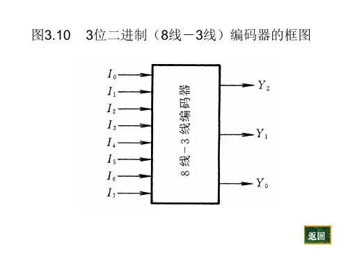
8线-3线编码器
- 格式:ppt
- 大小:154.00 KB
- 文档页数:10
自我检测题1.组合逻辑电路任何时刻的输出信号,与该时刻的输入信号 有关 ,与以前的输入信号 无关 。
2.在组合逻辑电路中,当输入信号改变状态时,输出端可能出现瞬间干扰窄脉冲的现象称为 竞争冒险 。
3.8线—3线优先编码器74LS148的优先编码顺序是7I 、6I 、5I 、…、0I ,输出为2Y 1Y 0Y 。
输入输出均为低电平有效。
当输入7I 6I 5I …0I 为时,输出2Y 1Y 0Y 为 010 。
4.3线—8线译码器74HC138处于译码状态时,当输入A 2A 1A 0=001时,输出07Y ~Y = 。
5.实现将公共数据上的数字信号按要求分配到不同电路中去的电路叫 数据分配器 。
6.根据需要选择一路信号送到公共数据线上的电路叫 数据选择器 。
7.一位数值比较器,输入信号为两个要比较的一位二进制数,用A 、B 表示,输出信号为比较结果:Y (A >B ) 、Y (A =B )和Y (A <B ),则Y (A >B )的逻辑表达式为B A 。
8.能完成两个一位二进制数相加,并考虑到低位进位的器件称为 全加器 。
9.多位加法器采用超前进位的目的是简化电路结构 × 。
(√,× ) 10.组合逻辑电路中的冒险是由于 引起的。
A .电路未达到最简 B .电路有多个输出C .电路中的时延D .逻辑门类型不同11.用取样法消除两级与非门电路中可能出现的冒险,以下说法哪一种是正确并优先考虑的A .在输出级加正取样脉冲B .在输入级加正取样脉冲C .在输出级加负取样脉冲D .在输入级加负取样脉冲12.当二输入与非门输入为 变化时,输出可能有竞争冒险。
A .01→10B .00→10C .10→11D .11→0113.译码器74HC138的使能端321E E E 取值为 时,处于允许译码状态。
A .011 B .100 C .101 D .01014.数据分配器和 有着相同的基本电路结构形式。
Verilog⼋线-三线优先编码器设计(74LS148)if语句法1//8线-3线优先编码器设计(74LS148)2//3//EI | A7 A6 A5 A4 A3 A2 A1 A0 | Y2 Y1 Y0 GS EO4//0 | 0 x x x x x x x | 0 0 0 0 15//0 | 1 0 x x x x x x | 0 0 1 0 16//0 | 1 1 0 x x x x x | 0 1 0 0 17//0 | 1 1 1 0 x x x x | 0 1 1 0 18//0 | 1 1 1 1 0 x x x | 1 0 0 0 19//0 | 1 1 1 1 1 0 x x | 1 0 1 0 110//0 | 1 1 1 1 1 1 0 x | 1 1 0 0 111//0 | 1 1 1 1 1 1 1 0 | 1 1 1 0 112//0 | 1 1 1 1 1 1 1 1 | 1 1 1 1 013//1 | x x x x x x x x | 1 1 1 1 1141516module encoder_83 (din, EI, GS, EO, dout);17input [7:0] din; //编码输⼊端data_in,低电平有效18input EI; //使能输⼊端EI(选通输⼊端),EI为 0 时芯⽚⼯作,即允许编码19output [2:0] dout; //编码输出端data_out20output GS; //⽚优先编码输出端,优先编码器⼯作⼯作状态标志GS,低电平有效21output EO; //使能输出端EO(选通输出端)22reg [2:0] dout;23reg GS, EO;24always @(din or EI)25if(EI) begin dout <= 3'b111; GS <= 1; EO <= 1; end //所有输出端被锁存在⾼电平26else if (din[7] == 0) begin dout <= 3'b000; GS <= 0; EO <= 1; end27else if (din[6] == 0) begin dout <= 3'b001; GS <= 0; EO <= 1; end28else if (din[5] == 0) begin dout <= 3'b010; GS <= 0; EO <= 1; end29else if (din[4] == 0) begin dout <= 3'b011; GS <= 0; EO <= 1; end30else if (din[3] == 0) begin dout <= 3'b100; GS <= 0; EO <= 1; end31else if (din[2] == 0) begin dout <= 3'b101; GS <= 0; EO <= 1; end32else if (din[1] == 0) begin dout <= 3'b110; GS <= 0; EO <= 1; end33else if (din[0] == 0) begin dout <= 3'b111; GS <= 0; EO <= 1; end34else if (din == 8'b11111111) begin dout <= 3'b111; GS <= 1; EO <= 0; end//芯⽚⼯作,但⽆编码输⼊35else begin dout <= 3'b111; GS <= 1; EO <= 1; end //消除锁存器(latch)36endmodule3738//EI = 0 表⽰允许编码,否则所有输出端被封锁在⾼电平(控制芯⽚⼯作)39//EO = 0 表⽰电路⼯作,但⽆编码输⼊(⽤于级联)40//GS = 0 表⽰电路⼯作,且有编码输⼊(判断输⼊端是否有输⼊)testbench:1 `timescale 1 ps/ 1 ps2module encoder_83_vlg_tst();3reg EI;4reg [7:0] din;5wire EO;6wire GS;7wire [2:0] dout;8 encoder_83 i1 (.EI(EI), .EO(EO), .GS(GS), .din(din), .dout(dout));9initial10begin11 EI = 1;12 din = 8'b11111111;13 #10 EI = 0;14 #10 din = 8'b01010101;15 #10 din = 8'b10101010;16 #10 din = 8'b11010101;17 #10 din = 8'b11101010;18 #10 din = 8'b11110101;19 #10 din = 8'b11111010;20 #10 din = 8'b11111101;21 #10 din = 8'b11111110;22 #10 din = 8'b11111111;23end24endmoduleView Codecase语句法1//8线-3线优先编码器设计(74LS148)2//3//EI | A7 A6 A5 A4 A3 A2 A1 A0 | Y2 Y1 Y0 GS EO4//0 | 0 x x x x x x x | 0 0 0 0 15//0 | 1 0 x x x x x x | 0 0 1 0 16//0 | 1 1 0 x x x x x | 0 1 0 0 17//0 | 1 1 1 0 x x x x | 0 1 1 0 18//0 | 1 1 1 1 0 x x x | 1 0 0 0 19//0 | 1 1 1 1 1 0 x x | 1 0 1 0 110//0 | 1 1 1 1 1 1 0 x | 1 1 0 0 111//0 | 1 1 1 1 1 1 1 0 | 1 1 1 0 112//0 | 1 1 1 1 1 1 1 1 | 1 1 1 1 013//1 | x x x x x x x x | 1 1 1 1 1141516module encoder_83_case (din, EI, GS, EO, dout);17input [7:0] din; //编码输⼊端data_in,低电平有效18input EI; //使能输⼊端EI(选通输⼊端),EI为 0 时芯⽚⼯作,即允许编码19output [2:0] dout; //编码输出端data_out20output GS; //⽚优先编码输出端,优先编码器⼯作⼯作状态标志GS,低电平有效21output EO; //使能输出端EO(选通输出端)22reg [2:0] dout;23reg GS, EO;24always @(din or EI)25if(EI)26begin dout <= 3'b111; GS <= 1; EO <= 1; end //所有输出端被锁存在⾼电平27else28casez (din) //建议⽤casez语句,casez把z/?匹配成任意。
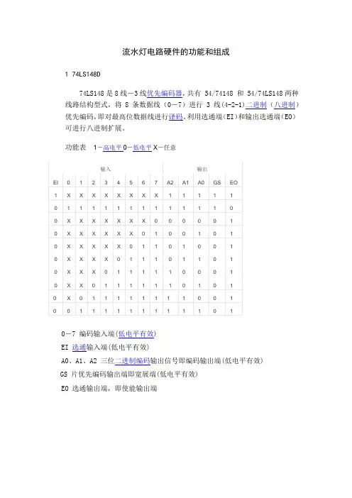
流水灯电路硬件的功能和组成1 74LS148D74LS148是8线-3线优先编码器,共有 54/74148 和 54/74LS148两种线路结构型式,将8条数据线(0-7)进行 3 线(4-2-1)二进制(八进制)优先编码,即对最高位数据线进行译码。
利用选通端(EI)和输出选通端(EO)可进行八进制扩展。
功能表0-7 编码输入端(低电平有效)EI 选通输入端(低电平有效)A0、A1、A2 三位二进制编码输出信号即编码输出端(低电平有效)GS 片优先编码输出端即宽展端(低电平有效)EO 选通输出端,即使能输出端图72.2 74LS138D74LS138 为3 线-8 线译码器,共有 54/74S138和 54/74LS138 两种线路结构型式,其74LS138工作原理如下:当一个选通端(G1)为高电平,另两个选通端(/(G2A)和/(G2B))为低电平时,可将地址端(A、B、C)的二进制编码在一个对应的输出端以低电平译出。
下图是它的原理结构图以及真值表:功能表表1无论从逻辑图还是功能表我们都可以看到74LS138的八个输出引脚,任何时刻要么全为高电平1--芯片处于不工作状态,要么只有一个为低电平0,其余7个输出引脚全为高电平1。
如果出现两个输出引脚同时为0的情况,说明该芯片已经损坏。
71LS138有三个附加的控制端、和。
当、时,输出为高电平(S=1),译码器处于工作状态。
否则,译码器被禁止,所有的输出端被封锁在高电平。
这三个控制端也叫做“片选”输入端,利用片选的作用可以将多篇连接起来以扩展译码器的功能。
2 74LS04D是个6反相器,整形,隔离,提升带负载能力的作用,即给输入引脚处提供高阻特性,使信号上升时间(上升沿陡峭程度)不受内部电路影响单片机集成电路芯片,是采用超大规模集成电路技术把具有数据处理能力的中央处理器CPU 随机存储器RAM、只读存储器ROM、多种I/O口和中断系统、定时器/计时器等功能(可能还包括显示驱动电路、脉宽调制电路、模拟多路转换器、A/D转换器等电路)集成到一块硅片上构成的一个小而完善的微型计算机系统,在工业控制领域的广泛应用。
自我检测题1.组合逻辑电路任何时刻的输出信号,与该时刻的输入信号 有关 ,与以前的输入信号 无关 。
2.在组合逻辑电路中,当输入信号改变状态时,输出端可能出现瞬间干扰窄脉冲的现象称为 竞争冒险 。
3.8线—3线优先编码器74LS148的优先编码顺序是7I 、6I 、5I 、…、0I ,输出为2Y 1Y 0Y 。
输入输出均为低电平有效。
当输入7I 6I 5I …0I 为11010101时,输出2Y 1Y 0Y 为 010 。
4.3线—8线译码器74HC138处于译码状态时,当输入A 2A 1A 0=001时,输出07Y ~Y = 11111101 。
5.实现将公共数据上的数字信号按要求分配到不同电路中去的电路叫 数据分配器 。
6.根据需要选择一路信号送到公共数据线上的电路叫 数据选择器 。
7.一位数值比拟器,输入信号为两个要比拟的一位二进制数,用A 、B 表示,输出信号为比拟结果:Y (A >B ) 、Y (A =B )和Y (A <B ),那么Y (A >B )的逻辑表达式为B A 。
8.能完成两个一位二进制数相加,并考虑到低位进位的器件称为 全加器 。
9.多位加法器采用超前进位的目的是简化电路结构 × 。
〔√,× 〕 10.组合逻辑电路中的冒险是由于 引起的。
A .电路未到达最简 B .电路有多个输出C .电路中的时延D .逻辑门类型不同11.用取样法消除两级与非门电路中可能出现的冒险,以下说法哪一种是正确并优先考虑的?A .在输出级加正取样脉冲B .在输入级加正取样脉冲C .在输出级加负取样脉冲D .在输入级加负取样脉冲12.当二输入与非门输入为 变化时,输出可能有竞争冒险。
A .01→10B .00→10C .10→11D .11→0113.译码器74HC138的使能端321E E E 取值为 时,处于允许译码状态。
A .011 B .100 C .101 D .01014.数据分配器和 有着相同的根本电路结构形式。

实验名称 8线-3线编码器设计指导老师尚丽娜成绩专业电科班级 1102 姓名汪磊学号31102333一、实验目的1、学习QuartusII软件,学习使用硬件描述语言设计电路。
2、学习DE1平台基本构成,能够使用DE1平台进行简单设计。
二、实验要求使用QuartusII文本输入法设计8线-3线编码器。
使用QuartusII软件进行文本输入,并对设计电路进行仿真,并下载到硬件平台,自行定义硬件平台使用端口。
三、实验设备PC机、DE1硬件平台四、实验原理根据8线—3线编码器的真值表原理进行实验,下表为8线—3线编码器的真值表五、实验过程library ieee;use ieee.std_logic_1164.all;entity bm8_3 isport(a:in std_logic_vector(7 downto 0);b:out std_logic_vector(2 downto 0));end bm8_3;architecture zhang of bm8_3 isbeginprocess(a)begincase a iswhen"00000001"=>b<="000";when"00000010"=>b<="001";when"00000100"=>b<="010";when"00001000"=>b<="011";when"00010000"=>b<="100";when"00100000"=>b<="101";when"01000000"=>b<="110";when others=>b<="111";end case;end process;end zhang;六、实验结果该程序还存在一些不足,当出现10000000是和非正常输入的时候是一样的输出,所以我们进行了一些修改,修改程序与结果如下:library ieee;use ieee.std_logic_1164.all;entity e isport(a:in std_logic_vector(7 downto 0);b:out std_logic_vector(3 downto 0));end e;architecture zhang of e isbeginprocess(a)begincase a iswhen"00000001"=>b<="0000";when"00000010"=>b<="0001";when"00000100"=>b<="0010";when"00001000"=>b<="0011";when"00010000"=>b<="0100";when"00100000"=>b<="0101";when"01000000"=>b<="0110";when"10000000"=>b<="0111";when others=>b<="1111";end case;end process;end zhang;思考题一:思考题二:entity e isport(a:in bit_vector(7 downto 0);b:out bit_vector(3 downto 0)); end e;architecture zhang of e isbeginprocess(a)begincase a iswhen"00000001"=>b<="0000";when"00000010"=>b<="0001";when"00000100"=>b<="0010";when"00001000"=>b<="0011";when"00010000"=>b<="0100";when"00100000"=>b<="0101";when"01000000"=>b<="0110";when"10000000"=>b<="0111";when others=>b<="1111";end case;end process;end zhang;七、心得体会对操作更加熟练,加深对其的认识。

实验报告
学院:专业:班级:
8'b0100_0000:led<=3'b110; //当输入信号是位宽为8位的二进制数据01000000时,输出信号为位宽
为3位的二进制数据110
8'b1000_0000:led<=3'b111; //当输入信号是位宽为8位的二进制数据时,输出信号为位宽为3位的
二进制数据111
default :led<=3'b000; //当输入信号是位宽为8位的二进制数据00000001时,输出信号为位宽
为3位的二进制数据000
endcase //结束分支语句
end //结束循环语句
endmodule //结束模块
实
验
数
据
上图为波形仿真。
如图可知,当输入信号为00000001时,输出信号为000;输入信号为00000010时,输出信号为001;
输入信号为00000100时,输出信号为010;输入信号为00001000时,输出信号为011;输入信号为00010000时,输出信号为100;输入信号为00100000时,输出信号为101;输入信号为01000000时,输出信号为
注:各学院可根据教学需要对以上栏木进行增减。
表格内容可根据内容扩充。
PACKAGING INFORMATIONOrderable Device Status(1)PackageType PackageDrawingPins PackageQtyEco Plan(2)Lead/Ball Finish MSL Peak Temp(3)78027012A ACTIVE LCCC FK201TBD Call TI Level-NC-NC-NC7802701EA ACTIVE CDIP J161TBD Call TI Level-NC-NC-NC7802701FA ACTIVE CFP W161TBD Call TI Level-NC-NC-NC JM38510/36001B2A ACTIVE LCCC FK201TBD Call TI Level-NC-NC-NC JM38510/36001BEA ACTIVE CDIP J161TBD Call TI Level-NC-NC-NC JM38510/36001BFA ACTIVE CFP W161TBD Call TI Level-NC-NC-NC SN54148J OBSOLETE CDIP J16TBD Call TI Call TISN54LS148J ACTIVE CDIP J161TBD Call TI Level-NC-NC-NCSN74147N OBSOLETE PDIP N16TBD Call TI Call TISN74148J OBSOLETE CDIP J16TBD Call TI Call TISN74148N OBSOLETE PDIP N16TBD Call TI Call TISN74148N3OBSOLETE PDIP N16TBD Call TI Call TISN74LS147DR OBSOLETE SOIC D16TBD Call TI Call TISN74LS147N OBSOLETE PDIP N16TBD Call TI Call TISN74LS148D ACTIVE SOIC D1640Green(RoHS&no Sb/Br)CU NIPDAU Level-1-260C-UNLIMSN74LS148DE4ACTIVE SOIC D1640Green(RoHS&no Sb/Br)CU NIPDAU Level-1-260C-UNLIMSN74LS148DR ACTIVE SOIC D162500Green(RoHS&no Sb/Br)CU NIPDAU Level-1-260C-UNLIMSN74LS148DRE4ACTIVE SOIC D162500Green(RoHS&no Sb/Br)CU NIPDAU Level-1-260C-UNLIM SN74LS148J OBSOLETE CDIP J16TBD Call TI Call TISN74LS148N ACTIVE PDIP N1625Pb-Free(RoHS)CU NIPDAU Level-NC-NC-NC SN74LS148N3OBSOLETE PDIP N16TBD Call TI Call TISN74LS148NE4ACTIVE PDIP N1625Pb-Free(RoHS)CU NIPDAU Level-NC-NC-NCSN74LS148NSR ACTIVE SO NS162000Green(RoHS&no Sb/Br)CU NIPDAU Level-1-260C-UNLIMSN74LS148NSRE4ACTIVE SO NS162000Green(RoHS&no Sb/Br)CU NIPDAU Level-1-260C-UNLIM SNJ54148J OBSOLETE CDIP J16TBD Call TI Call TISNJ54148W OBSOLETE CFP W16TBD Call TI Call TISNJ54LS148FK ACTIVE LCCC FK201TBD Call TI Level-NC-NC-NC SNJ54LS148J ACTIVE CDIP J161TBD Call TI Level-NC-NC-NC SNJ54LS148W ACTIVE CFP W161TBD Call TI Level-NC-NC-NC (1)The marketing status values are defined as follows:ACTIVE:Product device recommended for new designs.LIFEBUY:TI has announced that the device will be discontinued,and a lifetime-buy period is in effect.NRND:Not recommended for new designs.Device is in production to support existing customers,but TI does not recommend using this part in a new design.PREVIEW:Device has been announced but is not in production.Samples may or may not be available.OBSOLETE:TI has discontinued the production of the device.(2)Eco Plan-The planned eco-friendly classification:Pb-Free(RoHS)or Green(RoHS&no Sb/Br)-please check/productcontent for the latest availability information and additional product content details.TBD:The Pb-Free/Green conversion plan has not been defined.Pb-Free(RoHS):TI's terms"Lead-Free"or"Pb-Free"mean semiconductor products that are compatible with the current RoHS requirements for all6substances,including the requirement that lead not exceed0.1%by weight in homogeneous materials.Where designed to be soldered at high temperatures,TI Pb-Free products are suitable for use in specified lead-free processes.Green(RoHS&no Sb/Br):TI defines"Green"to mean Pb-Free(RoHS compatible),and free of Bromine(Br)and Antimony(Sb)based flame retardants(Br or Sb do not exceed0.1%by weight in homogeneous material)(3)MSL,Peak Temp.--The Moisture Sensitivity Level rating according to the JEDEC industry standard classifications,and peak solder temperature.Important Information and Disclaimer:The information provided on this page represents TI's knowledge and belief as of the date that it is provided.TI bases its knowledge and belief on information provided by third parties,and makes no representation or warranty as to the accuracy of such information.Efforts are underway to better integrate information from third parties.TI has taken and continues to take reasonable steps to provide representative and accurate information but may not have conducted destructive testing or chemical analysis on incoming materials and chemicals.TI and TI suppliers consider certain information to be proprietary,and thus CAS numbers and other limited information may not be available for release.In no event shall TI's liability arising out of such information exceed the total purchase price of the TI part(s)at issue in this document sold by TI to Customer on an annual basis.IMPORTANT NOTICETexas Instruments Incorporated and its subsidiaries (TI) reserve the right to make corrections, modifications, enhancements, improvements, and other changes to its products and services at any time and to discontinue any product or service without notice. Customers should obtain the latest relevant information before placing orders and should verify that such information is current and complete. All products are sold subject to TI’s terms and conditions of sale supplied at the time of order acknowledgment.TI warrants performance of its hardware products to the specifications applicable at the time of sale in accordance with TI’s standard warranty. T esting and other quality control techniques are used to the extent TI deems necessary to support this warranty. Except where mandated by government requirements, testing of all parameters of each product is not necessarily performed.TI assumes no liability for applications assistance or customer product design. Customers are responsible for their products and applications using TI components. T o minimize the risks associated with customer products and applications, customers should provide adequate design and operating safeguards.TI does not warrant or represent that any license, either express or implied, is granted under any TI patent right, copyright, mask work right, or other TI intellectual property right relating to any combination, machine, or process in which TI products or services are used. Information published by TI regarding third-party products or services does not constitute a license from TI to use such products or services or a warranty or endorsement thereof. Use of such information may require a license from a third party under the patents or other intellectual property of the third party, or a license from TI under the patents or other intellectual property of TI.Reproduction of information in TI data books or data sheets is permissible only if reproduction is without alteration and is accompanied by all associated warranties, conditions, limitations, and notices. Reproduction of this information with alteration is an unfair and deceptive business practice. TI is not responsible or liable for such altered documentation.Resale of TI products or services with statements different from or beyond the parameters stated by TI for that product or service voids all express and any implied warranties for the associated TI product or service and is an unfair and deceptive business practice. TI is not responsible or liable for any such statements. Following are URLs where you can obtain information on other Texas Instruments products and application solutions:Products ApplicationsAmplifiers Audio /audioData Converters Automotive /automotiveDSP Broadband /broadbandInterface Digital Control /digitalcontrolLogic Military /militaryPower Mgmt Optical Networking /opticalnetwork Microcontrollers Security /securityTelephony /telephonyVideo & Imaging /videoWireless /wirelessMailing Address:Texas InstrumentsPost Office Box 655303 Dallas, Texas 75265Copyright 2005, Texas Instruments Incorporated。
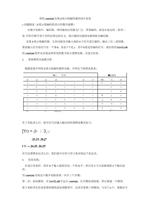
利用simulink实现8线3线编码器的设计仿真1问题描述(8线3线编码的设计的数学建模)在数字电路中,编码器、译码器的应用极为广泛。
所谓编码,就是在选定的一系列二值代码中赋予每个代码以固定的含义,执行编码功能的电路统称为编码器。
实现8线3线编码器,它的功能是对输入端的8个信号进行编码,输出三位二进制数。
要求输入信号每次只有一个事0,其余7个是1。
其中0值是待编码信号。
我们将用MATLAB 的simulink软件包实现这种常用的数字组合逻辑电路,并进行仿真。
2.系统模型及建模分析根据前面介绍的8线3线编码器的功能,可列出下面得真值表:有了真值表之后,就可以写出输入输出间的逻辑函数式如下:[Y O =J I・〕3心- J2.J3. J6.j7I Y- = J4.J5. J6.JT在写出逻辑表达式之后,我们就可以用与非门来实现这个表达式。
3.仿真实现;在进行仿真时,将在8个输入端依次加一个低电平,然后用3个示波器观察3个输出波形。
用simulink实现这个数学电路系统一共分三个步骤:第一步:添加模块,在MATLAB中运行simulink,打开模块浏览器,然后新建一个模型。
接下来把本次仿真需要的模块添加到模型中。
这里共需要三种模块:与非门4个,离散信号脉冲源8个,示波器3个。
与非门位于simulink模块库中的logocal operater,离散信号源脉冲位于simulink—sources—pulse generator, 示波器位于simulink—sinks—scope。
将这三种模块到拖到一个模型中。
点击与非门模块的名称,即写着Logical Operator的区域,将名称改为Y0,接着点击选中与非门模块不要松开鼠标,按住Ctrl键拖动这个模块到另一个位置,就会复制一个新的Y1模块。
用同样的方法得到Y2,类似地将离散信号脉冲源模块名字改为J0,同样得到J0,J1...J7。
最后将示波器复制三个。
自我检测题1.组合逻辑电路任何时刻的输出信号,与该时刻的输入信号 有关 ,与以前的输入信号 无关 。
2.在组合逻辑电路中,当输入信号改变状态时,输出端可能出现瞬间干扰窄脉冲的现象称为 竞争冒险 。
3.8线—3线优先编码器74LS148的优先编码顺序是7I 、6I 、5I 、…、0I ,输出为2Y 1Y 0Y 。
输入输出均为低电平有效。
当输入7I 6I 5I …0I 为时,输出2Y 1Y 0Y 为 010 。
4.3线—8线译码器74HC138处于译码状态时,当输入A 2A 1A 0=001时,输出07Y ~Y = 。
5.实现将公共数据上的数字信号按要求分配到不同电路中去的电路叫 数据分配器 。
6.根据需要选择一路信号送到公共数据线上的电路叫 数据选择器 。
7.一位数值比较器,输入信号为两个要比较的一位二进制数,用A 、B 表示,输出信号为比较结果:Y (A >B ) 、Y (A =B )和Y (A <B ),则Y (A >B )的逻辑表达式为B A 。
8.能完成两个一位二进制数相加,并考虑到低位进位的器件称为 全加器 。
9.多位加法器采用超前进位的目的是简化电路结构 × 。
(√,× ) 10.组合逻辑电路中的冒险是由于 引起的。
A .电路未达到最简 B .电路有多个输出C .电路中的时延D .逻辑门类型不同11.用取样法消除两级与非门电路中可能出现的冒险,以下说法哪一种是正确并优先考虑的?A .在输出级加正取样脉冲B .在输入级加正取样脉冲C .在输出级加负取样脉冲D .在输入级加负取样脉冲12.当二输入与非门输入为 变化时,输出可能有竞争冒险。
A .01→10B .00→10C .10→11D .11→0113.译码器74HC138的使能端321E E E 取值为 时,处于允许译码状态。
A .011 B .100 C .101 D .01014.数据分配器和 有着相同的基本电路结构形式。
实验二编码器实验目的1、设计并实现一个8线-3线优先编码器2、掌握实验箱的工作原理及基本操作方法实验器材1、SOPC实验箱2、计算机(装有Quartus II 7.0软件)实验预习1、预习优先编码器的原理与结构。
2、书写预习报告,必须有完整的VHDL设计程序及实验步骤。
实验原理常用的编码器有:4-2编码器、8-3编码器、16-4编码器,下面我们用一个8线-3线编码器的设计来介绍编码器的设计方法。
8-3编码器如图2.1所示,其真值表如表2-1所示。
图2.1 8-3编码器表2-1 8-3优先编码器真值表输入输出EIN 0N 1N 2N 3N 4N 5N 6N 7N A2N A1N A0N GSN EON1 X X X X X X X X 1 1 1 1 10 1 1 1 1 1 1 1 1 1 1 1 1 00 X X X X X X X 0 0 0 0 0 10 X X X X X X 0 1 0 0 1 0 10 X X X X X 0 1 1 0 1 0 0 10 X X X X 0 1 1 1 0 1 1 0 10 X X X 0 1 1 1 1 1 0 0 0 10 X X 0 1 1 1 1 1 1 0 1 0 10 X 0 1 1 1 1 1 1 1 1 0 0 10 0 1 1 1 1 1 1 1 1 1 1 0 1程序方法一Library IEEE;use IEEE.std_logic_1164.all;use IEEE.std_logic_unsigned.all;Entity B_bcd isport(D:in std_logic_vector(3 downto 0);B:out std_logic_vector(4 downto 0)); END Entity B_bcd;Architecture one of B_bcd isBeginProcess(D)BeginIF(D<="1001" AND D>="0000")Then B<='0'&D;ELSIF (D>"1001" AND D<="1111")Then B<=D+"00110";Else B<=NULL;END IF;END Process;END architecture one;程序方法2Library IEEE;use IEEE.std_logic_1164.all;use IEEE.std_logic_unsigned.all;Entity B_bcd isPort(D3,D2,D1,D0:in std_logic;B4,B3,B2,B1,B0:out std_logic);END entity B_bcd;Architecture one of B_bcd isSignal D:std_logic_vector(3 downto 0); Signal B:std_logic_vector(4 downto 0); BeginD<=D3 & D2 & D1 & D0;Process(D)BeginIF(D<="1001" AND D>="0000")Then B<='0'&D;ELSIF(D>"1001" AND D<="1111")Then B<=D+"00110";ELSE B<=NULL;END IF;END PROCESS;B0<=B(0);B1<=B(1); B2<=B(2); B3<=B(3); B4<=B(4);END architecture one;VCCSW4INPUT VCC SW3INPUT VCC SW2INPUT VCC SW1INPUT LED5OUTPUT LED4OUTPUT LED3OUTPUT LED2OUTPUT LED1OUTPUT D[3..0]B[4..0]B_bcdinst NOTinst5NOTinst6NOTinst7NOTinst8NOTinst9D [3..0]B [4..0]B[4..0]D[3..0]。
8线3线编码器原理
8线3线编码器是一种数字电路,用于将8个输入线的状态编码成3个输出线的状态。
它可以通过硬件电路实现,也可以使用编程语言来实现。
原理:
1. 共有8个输入线,每根输入线的状态可以是高电平(1)或低电平(0),总共有256种可能的输入状态。
2. 其中,只有其中一个输入线处于高电平状态,其他输入线都处于低电平状态的时候,对应的输出线才会处于高电平状态,其他输出线都处于低电平状态。
3. 输出线的状态也可以用二进制表示,3个输出线可以表示0到7的8个数字。
实现方法:
1. 可以使用逻辑门(如与门和或门)组合的方式来实现8线3线编码器。
根据输入线的状态,通过逻辑门的组合得到对应输出线的状态。
2. 可以根据输入状态使用编程语言来实现8线3线编码器。
使用条件语句(如if-else语句)判断输入状态,然后设置对应输出线的状态。
应用:
8线3线编码器常用于数字系统中,用于将多个输入信号编码成较少的输出信号。
它可以用于数据处理、控制系统等方面。
数字电子技术基础实验报告
实验二8线——3线优先编码器74LS148功能测试及应用
专业班级姓名学号成绩通信工程一班赵建倪201409110134
一、实验目的
了解8线——3线优先编码(74LS148)的基本功能;
掌握74LS148的使用方法;
二、实验内容
(1)了解芯片的工作原理
74LS148工作原理:该编码器有8个信号输入端,3个二进制码输出端。
此外,电路还设置了输入使能端EI,输出使能端EO和优先编码工作状态标志GS。
当EI=0时,编码器工作;而当EI=1时,则不论8个输入端为何种状态,3个输出端均为高电平,且优先标志端和输出使能端均为高电平,编码器处于非工作状态。
这种情况被称为输入低电平有效,输出也为低电来有效的情况。
当EI为0,且至少有一个输入端有编码请求信号(逻辑0)时,优先编码工作状态标志GS为0。
表明编码器处于工作状态,否则为1。
(2)了解芯片的结构,对照着具体的引脚接线
(3)验证优先编码器的真值表
真值表。