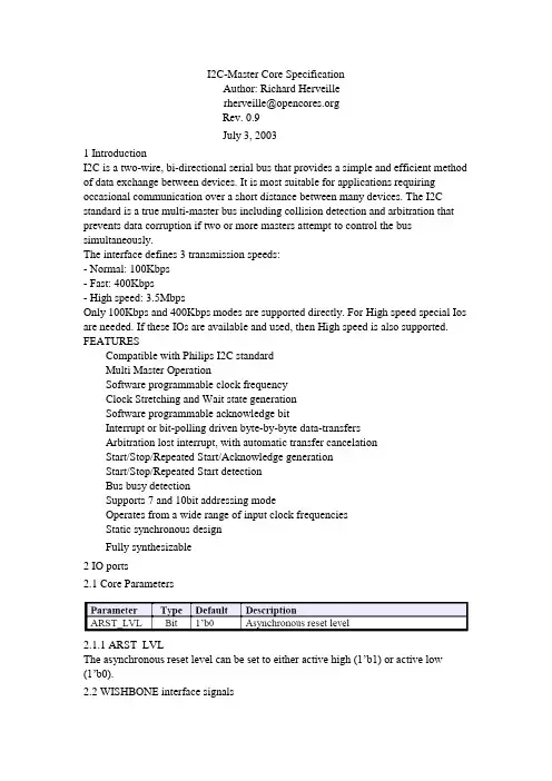
I2C-Master Core SpecificationAuthor: Richard Herveillerherveille@Rev. 0.9July 3, 20031 IntroductionI2C is a two-wire, bi-directional serial bus that provides a simple and efficient method of data exchange between devices. It is most suitable for applications requiring occasional communication over a short distance between many devices. The I2C standard is a true multi-master bus including collision detection and arbitration that prevents data corruption if two or more masters attempt to control the bus simultaneously.The interface defines 3 transmission speeds:- Normal: 100Kbps- Fast: 400Kbps- High speed: 3.5MbpsOnly 100Kbps and 400Kbps modes are supported directly. For High speed special Ios are needed. If these IOs are available and used, then High speed is also supported. FEATURESCompatible with Philips I2C standardMulti Master OperationSoftware programmable clock frequencyClock Stretching and Wait state generationSoftware programmable acknowledge bitInterrupt or bit-polling driven byte-by-byte data-transfersArbitration lost interrupt, with automatic transfer cancelationStart/Stop/Repeated Start/Acknowledge generationStart/Stop/Repeated Start detectionBus busy detectionSupports 7 and 10bit addressing modeOperates from a wide range of input clock frequenciesStatic synchronous designFully synthesizable2 IO ports2.1 Core Parameters2.1.1 ARST_LVLThe asynchronous reset level can be set to either active high (1’b1) or active low (1’b0).2.2 WISHBONE interface signalsThe core features a WISHBONE RevB.3 compliant WISHBONE Classic interface. All output signals are registered. Each access takes 2 clock cycles.arst_i is not a WISHBONE compatible signal. It is provided for FPGA implementations.Using [arst_i] instead of [wb_rst_i] can result in lower cell-usage and higher performance, because most FPGAs provide a dedicated asynchronous reset path. Use either [arst_i] or [wb_rst_i], tie the other to a negated state.2.3 External connectionsThe I2C interface uses a serial data line (SDA) and a serial clock line (SCL) for data transfers. All devices connected to these two signals must have open drain or open collector outputs. Both lines must be pulled-up to VCC by external resistors.The tri-state buffers for the SCL and SDA lines must be added at a higher hierarchical level. Connections should be made according to the following figure:For FPGA designs the compiler can automatically insert these buffers using the followingVHDL code:scl <= scl_pad_o when (scl_padoen_oe = ‘0’) else ‘Z’;sda <= s da_pad_o when (sda_padoen_oe = ‘0’) else ‘Z’;scl_pad_i <= scl;scl_pad_i <= sda;Verilog code:assign scl = scl_padoen_oe ? 1’bz : scl_pad_o;assign sda = sda_padoen_oe ? 1’bz: sda_pad_o;assign scl_pad_i = scl;assign sda_pad_i = sda;3Registers3.1 Registers list3.2 Register description3.2.1 Prescale RegisterThis register is used to prescale the SCL clock line. Due to the structure of the I2C interface, the core uses a 5*SCL clock internally. The prescale register must be programmed to this 5*SCL frequency (minus 1). Change the value of the prescale register only when the ‘EN’ bit is cleared.Example: wb_clk_i = 32MHz, desired SCL = 100KHz3.2.2 Control registerThe core responds to new commands only when the ‘EN’ bit is set. Pendingcommands ar e finished. Clear the ‘EN’ bit only when no transfer is in progress, i.e. after a STOP command, or when the command register has the STO bit set. When halted during a transfer, the core can hang the I2C bus.3.2.3 Transmit register3.2.4 Receive register3.2.5 Command registerThe STA, STO, RD, WR, and IACK bits are cleared automatically. These bits are alwaysread as zeros.3.2.6 Status register4.1 System ConfigurationThe I2C system uses a serial data line (SDA) and a serial clock line (SCL) for data transfers. All devices connected to these two signals must have open drain or open collector outputs. The logic AND function is exercised on both lines with external pull-up resistors.Data is transferred between a Master and a Slave synchronously to SCL on the SDA line on a byte-by-byte basis. Each data byte is 8 bits long. There is one SCL clock pulse for each data bit with the MSB being transmitted first. An acknowledge bit follows each transferred byte. Each bit is sampled during the high period of SCL; therefore, the SDA line may be changed only during the low period of SCL and must be held stable during the high period of SCL. A transition on the SDA line while SCL is high is interpreted as a command (see START and STOP signals).4.2 I2C ProtocolNormally, a standard communication consists of four parts:1) START signal generation2) Slave address transfer3) Data transfer4) STOP signal generation4.2.1 START signalWhen the bus is free/idle, meaning no master device is engaging the bus (both SCL and SDA lines are high), a master can initiate a transfer by sending a START signal.A START signal, usually referred to as the S-bit, is defined as a high-to-low transition of SDA while SCL is high. The START signal denotes the beginning of a new data transfer.A Repeated START is a START signal without first generating a STOP signal. The master uses this method to communicate with another slave or the same slave in a different transfer direction (e.g. from writing to a device to reading from a device)without releasing the bus.The core generates a START signal when the STA-bit in the Command Register is set and the RD or WR bits are set. Depending on the current status of the SCL line, a START or Repeated START is generated.4.2.2 Slave Address TransferThe first byte of data transferred by the master immediately after the START signal is the slave address. This is a seven-bits calling address followed by a RW bit. The RW bit signals the slave the data transfer direction. No two slaves in the system can have the same address. Only the slave with an address that matches the one transmitted by the master will respond by returning an acknowledge bit by pulling the SDA low at the 9th SCL clock cycle.Note: The core supports 10bit slave addresses by generating two address transfers. See the Philips I2C specifications for more details.The core treats a Slave Address Transfer as any other write action. Store the slave device’s address in the Transmit Register and set the WR bit. The core will then transfer the slave address on the bus.4.2.3 Data TransferOnce successful slave addressing has been achieved, the data transfer can proceed on a byte-by-byte basis in the direction specified by the RW bit sent by the master. Each transferred byte is followed by an acknowledge bit on the 9th SCL clock cycle. If the slave signals a No Acknowledge, the master can generate a STOP signal to abort the data transfer or generate a Repeated START signal and start a new transfer cycle.If the master, as the receiving device, does not acknowledge the slave, the slave releases the SDA line for the master to generate a STOP or Repeated START signal. To write data to a slave, store the data to be transmitted in the Transmit Register and set the WR bit. To read data from a slave, set the RD bit. During a transfer the core set the TIP flag, indicating that a Transfer is In Progress. When the transfer is done the TIP flag is reset, the IF flag set and, when enabled, an interrupt generated. The Receive Register contains valid data after the IF flag has been set. The user may issuea new write or read command when the TIP flag is reset.4.2.4 STOP signalThe master can terminate the communication by generating a STOP signal. A STOPsignal, usually referred to as the P-bit, is defined as a low-to-high transition of SDA while SCL is at logical ‘1’.4.3 Arbitration Procedure4.3.1 Clock SynchronizationThe I2C bus is a true multimaster bus that allows more than one master to be connected on it. If two or more masters simultaneously try to control the bus, a clock synchronization procedure determines the bus clock. Because of the wired-AND connection of the I2C signals a high to low transition affects all devices connected to the bus. Therefore a high to low transition on the SCL line causes all concerned devices to count off their low period. Once a device clock has gone low it will hold the SCL line in that state until the clock high state is reached. Due to the wired-AND connection the SCL line will therefore be held low by the device with the longest low period, and held high by the device with the shortest high period.4.3.2 Clock StretchingSlave devices can use the clock synchronization mechanism to slow down the transfer bit rate. After the master has driven SCL low, the slave can drive SCL low for the required period and then release it. If the slave’s SCL low period is greater than the master’s SCL low period, the resulting SCL bus signal low period is stretched, thus inserting waitstates.5 ArchitectureThe I2C core is built around four primary blocks; the Clock Generator, the Byte Command Controller, the Bit Command Controller and the DataIO Shift Register.All other blocks are used for interfacing or for storing temporary values.5.1 Clock GeneratorThe Clock Generator generates an internal 4*Fscl clock enable signal that triggers all synchronous elements in the Bit Command Controller. It also handles clock stretching needed by some slaves.5.2 Byte Command ControllerThe Byte Command Controller handles I2C traffic at the byte level. It takes data from the Command Register and translates it into sequences based on the transmission of a single byte. By setting the START, STOP, and READ bit in the Command Register, for example, the Byte Command Controller generates a sequence that results in the generation of a START signal, the reading of a byte from the slave device, and the generation of a STOP signal. It does this by dividing each byte operation into separatebit-operations, which are then sent to the Bit Command Controller.5.3 Bit Command ControllerThe Bit Command Controller handles the actual transmission of data and the generation of the specific levels for START, Repeated START, and STOP signals by controlling the SCL and SDA lines. The Byte Command Controller tells the Bit Command Controller which operation has to be performed. For a single byte read, the Bit Command Controller receives 8 separate read commands. Each bit-operation is divided into 5 pieces (idle and A, B, C, and D), except for a STOP operation which is divided into 4 pieces (idle and A,B, and C).5.4 DataIO Shift RegisterThe DataIO Shift Register contains the data associated with the current transfer. During a read action, data is shifted in from the SDA line. After a byte has been read the contents are copied into the Receive Register. During a write action, the Transmit Register’s contents are copied into the DataIO Shift Register and are then transmitted onto the SDA line.6 Programming examplesExample 1Write 1 byte of data to a slave.Slave addr ess = 0x51 (b”1010001”)Data to write = 0xACI2C Sequence:1) generate start command2) write slave address + write bit3) receive acknowledge from slave4) write data5) receive acknowledge from slave6) generate stop commandCommands:1) write 0xA2 (address + write bit) to Transmit Register, set STA bit, set WR bit.-- wait for interrupt or TIP flag to negate --2) read RxACK bit from Status Register, should be ‘0’.write 0xAC to Transmit register, set STO bit, set WR bit.-- wait for interrupt or TIP flag to negate --3) read RxACK bit from Status Register, should be ‘0’.Example 2Read a byte of data from an I2C memory device.Slave address = 0x4EMemory location to read from = 0x20I2C sequence:1) generate start signal2) write slave address + write bit3) receive acknowledge from slave4) write memory location5) receive acknowledge from slave6) generate repeated start signal7) write slave address + read bit8) receive acknowledge from slave9) read byte from slave10) write no acknowledge (NACK) to slave, indicating end of transfer11) generate stop signalCommands:1) write 0x9C (address + write bit) to Transmit Register, set STA bit, set WR bit. -- wait for interrupt or TIP flag to negate --2) read RxACK bit from Sta tus Register, should be ‘0’.write 0x20 to Transmit register, set WR bit.-- wait for interrupt or TIP flag to negate --3) read RxACK bit from Status Register, should be ‘0’.write 0x9D (address + read bit) to Transmit Register, set STA bit, set WR bit.-- wait for interrupt or TIP flag to negate --4) set RD bit, set ACK to ‘1’ (NACK), set STO bitAppendix ASynthesis results Synthesis tool: Synplify Pro。