用户手册STM8S-DISCOVERY
- 格式:pdf
- 大小:327.42 KB
- 文档页数:17
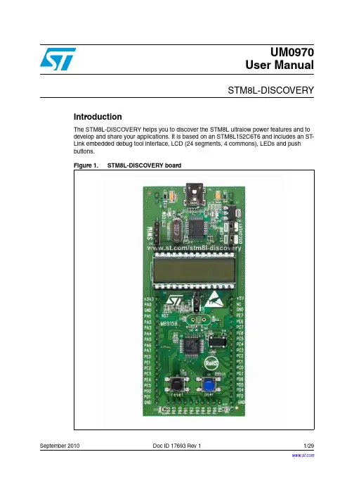
UM0970User ManualSTM8L-DISCOVERYIntroductionThe STM8L-DISCOVERY helps you to discover the STM8L ultralow power features and todevelop and share your applications. It is based on an STM8L152C6T6 and includes an ST-Link embedded debug tool interface, LCD (24 segments, 4 commons), LEDs and pushbuttons.Figure 1.STM8L-DISCOVERY boardSeptember 2010Doc ID 17693 Rev 11/29Contents UM0970Contents1Quick start . . . . . . . . . . . . . . . . . . . . . . . . . . . . . . . . . . . . . . . . . . . . . . . . . 31.1Getting started . . . . . . . . . . . . . . . . . . . . . . . . . . . . . . . . . . . . . . . . . . . . . . 31.2System requirements . . . . . . . . . . . . . . . . . . . . . . . . . . . . . . . . . . . . . . . . . 31.3Development toolchain . . . . . . . . . . . . . . . . . . . . . . . . . . . . . . . . . . . . . . . . 41.4Demonstration software . . . . . . . . . . . . . . . . . . . . . . . . . . . . . . . . . . . . . . . 41.5Order code . . . . . . . . . . . . . . . . . . . . . . . . . . . . . . . . . . . . . . . . . . . . . . . . . 4 2Features . . . . . . . . . . . . . . . . . . . . . . . . . . . . . . . . . . . . . . . . . . . . . . . . . . . 53Hardware and layout . . . . . . . . . . . . . . . . . . . . . . . . . . . . . . . . . . . . . . . . . 63.1STM8L152C6T6 microcontroller . . . . . . . . . . . . . . . . . . . . . . . . . . . . . . . . 93.2Embedded ST-Link . . . . . . . . . . . . . . . . . . . . . . . . . . . . . . . . . . . . . . . . . . 113.2.1Using the ST-Link to program/debug the STM8L on board . . . . . . . . . . 123.2.2Using the ST-Link to program/debug an external STM8L application . . 123.3Power supply and power selection . . . . . . . . . . . . . . . . . . . . . . . . . . . . . . 133.4LEDs . . . . . . . . . . . . . . . . . . . . . . . . . . . . . . . . . . . . . . . . . . . . . . . . . . . . 133.5Push buttons . . . . . . . . . . . . . . . . . . . . . . . . . . . . . . . . . . . . . . . . . . . . . . 133.6Built-in IDD measurement circuit . . . . . . . . . . . . . . . . . . . . . . . . . . . . . . . 143.6.1Run mode . . . . . . . . . . . . . . . . . . . . . . . . . . . . . . . . . . . . . . . . . . . . . . . 143.6.2Low power mode . . . . . . . . . . . . . . . . . . . . . . . . . . . . . . . . . . . . . . . . . . 143.6.3Low power mode I DD measurement principle . . . . . . . . . . . . . . . . . . . . 153.6.4Ibias current measurement procedure . . . . . . . . . . . . . . . . . . . . . . . . . . 163.7Solder bridges . . . . . . . . . . . . . . . . . . . . . . . . . . . . . . . . . . . . . . . . . . . . . 163.8LCD (24 segments, 4 commons) . . . . . . . . . . . . . . . . . . . . . . . . . . . . . . . 17 4Extension connection . . . . . . . . . . . . . . . . . . . . . . . . . . . . . . . . . . . . . . . 19 5Electrical schematics . . . . . . . . . . . . . . . . . . . . . . . . . . . . . . . . . . . . . . . 23 6Revision history . . . . . . . . . . . . . . . . . . . . . . . . . . . . . . . . . . . . . . . . . . . 282/29Doc ID 17693 Rev 1UM0970Quick startDoc ID 17693 Rev 13/291 Quick startThe STM8L-DISCOVERY is a low-cost and easy-to-use development kit to quickly evaluateand start a development with an STM8L ultralow power microcontroller.Before installing and using the product, please accept the Evaluation Product License Agreement from /stm8l-discovery.For more information on the STM8L-DISCOVERY and for demonstration software visit /stm8l-discovery.1.1 Getting started1.Check jumper positions on the board, JP1 and CN3 ON (Discovery selected).2. Connect the STM8L-DISCOVERY board to a PC with a USB cable to power the board.Red LED LD2 (PWR) then lights up.3.Function 1 is executed and each click on user button B2 changes the executed function as described in Table 1.To study or modify the DISCOVER project related to this demo, visit /stm8l-discovery and follow the tutorial. Discover the STM8L features, download and execute programs proposed in the list of projects. This site also contains examples from which you can develop your own applications.1.2 System requirements●Windows PC (2000, XP , Vista)●A/Mini-B USB cableTable 1.FunctionsFunction LED LD3/4BarsValue displayed1BlinkSTM8L V DD voltage measured2Off STM8L consumption measured in Run mode3Off STM8L consumption measured in Low power mode, LCD on4Off STM8L consumption measured in Low power mode, LCD off5Off STM8L consumption measured in Halt mode, LCD offQuick start UM09704/29Doc ID 17693 Rev 11.3 Development toolchain●IAR, Embedded Workbench® for STM8●STMicroelectronics, ST Visual Develop (STVD)1.4 Demonstration softwareDemonstration software is preloaded in the board's Flash memory. This demonstration usesthe built-in IDD measurement feature of the STM8L-DISCOVERY to automatically measure and display on the LCD the consumption of the MCU in run and low power modes. The latest versions of this demonstration source code and associated documentation can be downloaded from /stm8l-discovery.1.5 Order codeTo order the STM8L ultralow power Discovery, use the order code STM8L-DISCOVERY.UM0970FeaturesDoc ID 17693 Rev 15/292 FeaturesThe STM8L-DISCOVERY offers the following features:●STM8L152C6T6 microcontroller, 32 KB Flash, 2 KB RAM, 1KB EEPROM in 48-pin LQFP●On-board ST -Link with selection mode switch to use the kit as a stand-alone ST -Link (with SWIM connector for programming and debugging)●Two red LEDs; LD1 for USB communication, LD2 for 3.3 V power on ●Designed to be powered by USB or an external supply of 5 V or 3.3 V ●Can supply target application with 5 volts and 3 volts ●Two user LEDs, LD3 and LD4 (green and blue)●Two push buttons (User and Reset)●I DD current measurement●LCD 28-pin DIP (24 segments, 4 commons)●Extension header for all QFP48 I/Os for quick connection to prototyping board for easy probingHardware and layout UM0970 3 Hardware and layoutThe STM8L-DISCOVERY is designed around the STM8L152C6T6 microcontroller in a 48-pin LQFP package.Figure2 illustrates the connections between the STM8L152C6T6 and its peripherals (ST-Link, push button, LED, LCD and connectors).Figure3 and Figure4 help you to locate these features on the STM8L-DISCOVERY.6/29Doc ID 17693 Rev 1UM0970Hardware and layoutDoc ID 17693 Rev 17/29Figure 3.Top layoutST -LinkLCD 24 segmentsI DD measurement STM8L152C6T6B2CN2JP1LD3LD4B1CN3IDD moduleLD1LD2User buttonLED blueReset buttonLED greenSWIM connectorCOMpowerSB1,2X2 crystalD2 diode D1 diodeST -Link/Discovery selector+3.3V power supply input+5Vpower supply inputHardware and layoutUM09708/29Doc ID 17693 Rev 1Figure 4.Bottom layoutP1P2SB4,6,8,10PRG-32SB3,5,7,9DEFAULTSB11,12,14SB13,15SB16SB17P3IDD_MeasurementB2-USER B1-RESETX3 crystal connectorconnectorconnectorJP1IDD(RESERVED)UM0970Hardware and layoutDoc ID 17693 Rev 19/293.1 STM8L 152C6T6 microcontrollerThis 8-bit ultralow power MCU has 32 KB Flash, 2 KB RAM, 1 KB data EEPROM, RTC,LCD, timers, USART, I2C, SPI, ADC, DAC and comparators.Figure 5.STM8L152C6T6 packageThis device provides the following benefits:●Ultralow power proprietary 130 nm technology:Speed and power consumption independent of MCU power supply, Ultralow leakage ●Ultralow power design (clock gating, low-power Flash with power-off capability): Reduced overall Run and Wait mode current consumption by turning off clocks of unused peripherals or Flash●Sub 1µA hardware RTC and AWU system unit:Ultralow power modes for applications requesting regular wake up●Range of Low power modes (up to 4):Suitable for many applications from complete switch off to continuous monitoring at ultralow frequency●Advanced and flexible clock system (multiple internal and external clock sources): Switch and adjust frequency and clock sources on the fly depending on application needs●Direct memory access on board (4-channel DMA):Autonomy for peripherals, independent from core; can switch off Flash memory and CPU (large current consumption contributors) while keeping peripherals active ●Ultralow power and ultrasafe reset system POR/PDR; additional optional activationBOR:Integrated safety and security for application●Ultrafast wakeup from lowest Low power mode (4µs): Fast switching from Static and Dynamic power modes●Analog functional down to 1.8 V, programming down to 1.65 V: Full functionality over the complete V DD rangeFor more information see the STM8L152C6T6 datasheet (Doc ID 15962) on the ST website.The STM8L152C6T6 8-bit microcontroller offers: 2Kbytes RAM32Kbytes of Flash memory LQFP48 7 x 7 mm1Kbytes EEPROMHardware and layout UM0970 Figure 6.STM8L152C6T6 block diagram10/29Doc ID 17693 Rev 1UM0970Hardware and layoutDoc ID 17693 Rev 111/293.2 Embedded ST-LinkThe ST -Link programming and debugging tool is integrated on the STM8L-DISCOVERY.The embedded ST -Link can be used in 2 different ways according to the jumper states (see Table 2):●to program/debug the MCU on board,●to program/debug an MCU in an external application board using a cable connected to SWIM connector CN2.For information about debugging and programming features refer to ST -Link UM0627.Note:UM0627 contains information about all the ST -Link features. Usage in this situation is restricted to STM8 devices and SWIM support.Figure 7.Typical configurationTable 2.Jumper statesJumper stateDescriptionBoth CN3 jumpers ON ST -Link functions enabled for on board programming (default)Both CN3 jumpers OFFST -Link functions enabled for external application through CN2 connector (SWIM supported).Hardware requirements:- USB cable type A to mini-B- Computer with Windows 2000, XP or Vista OSDevelopment toolchain:- IAR, Embedded Workbench® for STM8L- STMicroelectronics, ST Visual Develop (STVD)Hardware and layout UM09703.2.1 Using the ST-Link to program/debug the STM8L on boardTo program the STM8L on board, simply plug in the two jumpers on CN3, as shown inFigure8 in red, but do not use the CN2 connector as that could disturb communication withthe STM8L152C6T6 of the STM8L-DISCOVERY.Figure 8.STM8L-DISCOVERY connections imageJumpers on CN33.2.2 Using the ST-Link to program/debug an external STM8L applicationIt is very easy to use the ST-Link to program the STM8L on an external application. Simplyremove the 2 jumpers from CN3 as shown in Figure9, and connect your application to theCN2 debug connector according to Table3.Table 3.Debug connector CN2 (SWIM)Pin CN2Designation1VDD_TARGET VDD from application2SWIM SWIM data input/output3GND Ground4SWIM_RST SWIM reset12/29Doc ID 17693 Rev 1UM0970Hardware and layoutDoc ID 17693 Rev 113/29Figure 9.ST-Link connections image3.3 Power supply and power selectionThe power supply is provided either by the host PC through the USB cable, or by external power supply (5V or 3.3V). The D1 and D2 protection diodes allow the 5V and 3V3 pins to be used independently as input or output power supplies (see Figure 3). The 5V and 3V3 pins can be used as an output power supply for use by an application board connected on pin headers (P1 to P3). In such a case, the 3V3 pin provides only a 3V power supply and the power consumption must be lower than 100mA. The 5V and 3V3 pins can also be used as an input power supply for the board when the USB connector is not connected to the PC.3.4 LEDs●LD1 COM: Red LED indicates communication in progress between PC and ST -Link.●LD2 PWR: Red LED indicates that the board is powered.●LD3 PE7: Green LED is a user LED connected to the I/O PE7 of the STM8L152C6T6.●LD4 PC7: Blue LED is a user LED connected to the I/O PC7 of the STM8L152C6T6.3.5 Push buttons●B1 RST: Push button is used to RESET the STM8L152C6T6.●B2 USER: User push button connected to the I/O PC1 of the STM8L152C6T6.No jumpers on CN3Hardware and layout UM097014/29Doc ID 17693 Rev 13.6 Built-in IDD measurement circuitThe STM8L-DISCOVERY built-in I DD measurement circuit allows the consumption of the STM8L152C6T6 to be measured and displayed on the LCD Glass while the MCU is in Run or Low power saving modes.●JP1 in ON position: STM8L152C6T6 is powered through I DD measurement circuit (default).●JP1 in OFF position: STM8L152C6T6 is powered directly by +3V3, I DD measurement circuit is bypassed.Note:When jumper JP1 is removed the current consumption of the STM8L152C6T6 can be measured by connecting an ammeter between jumper JP1 pin 1 and pin 2.For Imeasurement by the MCU itself, the circuit below is implemented on the STM8L-measurement timing according to Figure 11.UM0970Hardware and layout 3.6.3 Low power mode I DD measurement principleThe principle used to measure a current when the STM8L152C6T6 is in Low power mode is:1.Configure ADC to measure voltage on the IDD_Measurement pin.2. Configure PE6 to serve as wakeup pin.3. Enter Low power mode after setting IDD_CNT_EN (PC4) signal low.4. IDD_WAKEUP rising edge wakes up the MCU after around 300ms.5. Start ADC conversion as soon as possible after wakeup in order to measure thevoltage corresponding to Low power mode on capacitor C11.6. Reset the counter by programming IDD_CNT_EN high (in less than 70ms after thewakeup) to avoid the R21 2KΩ resistor being connected later in Run mode.The measurement timing is given in Figure11. In Low power modes, the 2KΩ resistor isconnected when T1 goes off after entering Low power mode. Q13 output of the counterallows connection of the 2KΩ resistor when the current I DD becomes very low.Figure11 shows how the counter and T1 ensure that, 150ms after IDD_CNT_EN fallingedge, the shunt resistor R21 is connected between VDD_MCU and the power supply inorder to reduce the measurement range to 30uA full scale. Then after another 150ms forcurrent stabilization, R21 is shorted, the IDD measurement is stored in C11, and the MCU iswoken up. After wakeup the MCU can measure the IDD current corresponding to the Lowpower mode stored in C11.Figure 11.STM8L-DISCOVERY I DD Low power mode measurement timing diagramThe Low power mode measurement procedure can be used in Halt or Active halt mode if theI DD current does not exceed 30uA, otherwise the I DD measurement procedure in Run modeshould be used up to 30mA.Doc ID 17693 Rev 115/29Hardware and layout UM097016/29Doc ID 17693 Rev 13.6.4 Ibias current measurement procedureIn Low power mode the bias current of operational amplifier input (U4 pin 4) is not negligiblecompared to I DD current (typical Ibias is ~240 nA). T o obtain a reliable STM8L152 I DD measurement it is mandatory to subtract the bias current from the I DD low power measurement since this current is not sinked by the MCU. Ibias is measured duringproduction test and stored in the MCU EPROM. The demonstration software, Discover, uses this value to display the correct I DD . The Ibias measurement procedure is part of the demonstration software and can be launched if required.The procedure for Ibias measurement (implemented in the Demo) is:1.Power off the board (disconnect the USB cable).2. Set jumper JP1 to OFF position (pins 1 and 2).3. Push down B2 (USER button), power on the board from the USB.4. Wait at least 1 second before releasing B2, the LCD displays the Ibias measurement.5. Power off the board (disconnect the USB cable).6.Set jumper JP1 to ON position (pins 2 and 3). The Ibias value is now stored. The bias current is then subtracted from the I DD measurement performed in Low power mode.3.7 Solder bridgesTable 4.Solder bridgeBridgeState (1)1.Default state is in bold type.DescriptionSB1,2(X2 crystal)Off P A2, P A3 are disconnected from P1X2, C19, C20 and R24 provide a clock as shown in schematics On P A2, P A3 are connected to P1 (X2, C19, C20, R24 must not be fitted)SB3,5,7,9 (DEFAULT)On Reserved, do not modify SB4,6,8,10(PRG-32)Off Reserved, do not modifySB11,12,14(IDD_Measurement)Off PFO, PE6, PC4 are available and IDD module cannot be used JP1 must be set to OFFOn PFO, PE6, PC4 are used by IDD module JP1 must be set to ONSB13,15(X3 crystal)Off PC5, PC6 are only connected to P2 (but do not remove X3, C21, C23, R27)On PC5, PC6 are connected to P2. X3, C21, C23 and R27 provide 32KHz clock SB16(B1-RESET)Off P A1/RESET signal is only connected to P1On P A1/RESET signal is used by ST_LINK as SWIM_RST and also connected to P1SB17(B2-USER)Off PC1 is only connected to P2OnPC1 is connected to P2 and push button B2 for userUM0970Hardware and layout3.8 LCD (24 segments, 4 commons)This LCD allows the STM8L152C6T6 to display any information on six 14-segment digitsand 4 BARs, using all COMs. (See the LCD segment mapping in Figure12 and pinconnections in Table5.)Note:This LCD also supports six 8-segment digits by only using COM0 and COM1.This configuration allows COM2 and COM3 to be used as I/O ports. In this case the 2 LCDpins must not be plugged into the LCD socket. To proceed with this configuration, removethe LCD carefully, slightly open the COM2 and COM3 pins (pin 13 and pin 14) of the LCD,then replug it in the socket.Characteristics overview:●24 segments and 4 commons●Drive method: multiplexed 1/4 duty, 1/3 bias●Operating voltage: 3V●Operating temperature: 0 to 50°C●Connector: 28-pin DIL 2.54mm pitchNote:When the LCD is plugged, all I/O ports listed in Table5 are unavailable. To use one of these as I/O, you must remove the LCD.Figure 12.LCD segment mappingDoc ID 17693 Rev 117/29Hardware and layout UM0970Table 5.LCD connectionsSTM8L152C6T6 LCDPin name Pin COM3COM2COM1COM0 P A7_LCDSEG011N1P1D1EPE0_LCDSEG121DP1COLON1C1MPE1_LCDSEG232N2P2D2EPE2_LCDSEG342DP2COLON2C2MPE3_LCDSEG453N3P3D3EPE4_LCDSEG563DP3COLON3C3MPE5_LCDSEG674N4P4D4EPD0_LCDSEG784DP4COLON4C4MPD2_LCDSEG895N5P5D5EPD3_LCDSEG910BAR2BAR35C5MPB0_LCDSEG10116N6P6D6EPB1_LCDSEG1112BAR0BAR16C6MPD1_LCDCOM313COM3P A6_LCDCOM214COM2P A5_LCDCOM115COM1P A4_LCDCOM016COM0PB2_LCDSEG12176J6K6A6BPB3_LCDSEG13186H6Q6F6GPB4_LCDSEG14195J5K5A5BPB5_LCDSEG15205H5Q5F5GPB6_LCDSEG16214J4K4A4BPB7_LCDSEG17224H4Q4F4GPD4_LCDSEG18233J3K3A3BPD5_LCDSEG19243H3Q3F3GPD6_LCDSEG20252J2K2A2BPD7_LCDSEG21262H2Q2F2GPC2_LCDSEG22271J1K1A1BPC3_LCDSEG23281H1Q1F1G18/29Doc ID 17693 Rev 1Extension connection UM097019/29Doc ID 17693 Rev 14 Extension connectionMale headers P1, P2 and P3 can connect the STM8L-DISCOVERY to a standardprototyping/wrapping board. All GPI/Os of STM8L152C6T6 are available on it.P1, P2 and P3 can also be probed by an oscilloscope, logical analyzer or voltmeter.Table 6.P1 pinoutPin number (P1)Pin number(STM8L)Board pin nameT y p eMain functionAlternate function LCD (U5)1+3V33.3 V board power supplied or supplyexternal application when USB connected21P A0I/O Port A0 P A0/[USART1_CK](3)/SWIM/BEEP/IR_TIM (7)39/40GND Ground42P A1I/O ResetNRST/P A1(1)53P A2I/O Port A2 P A2/OSC_IN/[USART1_TX](3)/[SPI1_MISO] (3) 64P A3I/O Port A3 P A3/OSC_OUT/[USART1 _RX](3)/[SPI1_MOSI](3) 75P A4I/O Port A4P A4/TIM2_BKIN/ LCD_COM0(2)/ADC1_IN2/COMP1_INP LCD_COM086P A5I/O Port A5P A5/TIM3_BKIN/ LCD_COM1(2)/ADC1_IN1/COMP1_INP LCD_COM197P A6I/O Port A6P A6/[ADC1_TRIG](3)/LCD_COM2(2)/ADC1_IN0/ COMP1_INP LCD_COM2108P A7I/O Port A7 P A7/LCD_SEG0(2)(4) LCD_SEG01114PE0I/O Port E0 PE0(4)/LCD_SEG1(2) LCD_SEG11215PE1I/O Port E1 PE1/TIM1_CH2N / LCD_SEG2(2) LCD_SEG21316PE2I/O Port E2PE2/TIM1_CH3N / LCD_SEG3(2)LCD_SEG31417PE3I/O Port E3 PE3/LCD_SEG4(2) LCD_SEG41518PE4I/O Port E4 PE4/LCD_SEG5(2)LCD_SEG5UM0970Extension connectionDoc ID 17693 Rev 120/291619PE5I/O Port E5PE5/LCD_SEG6(2)/ADC1_IN23/COMP2_INP/ COMP1_INP LCD_SEG61720PD0I/O Port D0PD0/TIM3_CH2/ [ADC1_TRIG](3)/ LCD_SEG7(2)/ADC1_IN2 2/COMP2_INP/ COMP1_INP LCD_SEG71821PD1I/O Port D1 PD1/TIM3_TRIG/ LCD_COM3(2)/ADC1_IN21/COMP2_INP/ COMP1_INPLCD_COM3199/40GNDGroundTable 7.P2 pinoutPin number (P2)Pin number(STM8L)Pin nameT y p eMain functionAlternate function LCD (U5)1+5V5 Volts board power supplied or supplyexternal application when USB connected2NC 39/40GND Ground448PE7I/O Port E7 PE7/LCD_SEG27(2)547PE6 I/O Port E6PE6/LCD_SEG26(2)/PVD_IN646PC7I/O Port C7PC7/LCD_SEG25(2)/ ADC1_IN3/COMP2_INM/ COMP1_INP 745PC6I/O Port C6PC6/OSC32_OUT/ [SPI1_SCK](3)/ [USART1_RX](3)844PC5I/O Port C5 PC5/OSC32_IN /[SPI1_NSS](3)/[USART1_TX](3) 943PC4I/O Port C4 PC4/[USART1_CK](3)/ I2C1_SMB/CCO/LCD_SEG24(2)/ADC1_IN4/COMP2_INM/ COMP1_INPTable 6.P1 pinout (continued)Pin number (P1)Pin number(STM8L)Board pin nameT y p eMain functionAlternate function LCD (U5)UM0970Extension connectionDoc ID 17693 Rev 121/291042PC3I/O Port C3 PC3/[USART1_TX](3)/LCD_SEG23(2)/ADC1_IN5/COMP1_INP/ COMP2_INM LCD_SEG231141PC2I/O Port C2 PC2/[USART1_RX](3)/ LCD_SEG22/ADC1_IN6/COMP1_INP/VREF_OUT LCD_SEG221238PC1I/O Port C1 PC1(4)/I2C1_SCL 1337PC0I/O Port C0 PC0(4)/I2C1_SDA1436PD7I/O Port D7 PD7/TIM1_CH1N /LCD_SEG21(2)/ ADC1_IN7/RTC_ALARM/ VREF_OUT/ COMP1_INPLCD_SEG211535PD6I/O Port D6PD6/TIM1_BKIN /LCD_SEG20(2)/ ADC1_IN8/RTC_CALIB/ VREF_OUT/ COMP1_INP LCD_SEG201634PD5I/O Port D5PD5/TIM1_CH3 /LCD_SEG19(2)/ADC1_IN9/COMP1_INP LCD_SEG191733PD4I/O Port D4PD4/TIM1_CH2 /LCD_SEG18(2)/ADC1_IN10/COMP1_INP LCD_SEG181832PF0I/O Port F0PF0/ADC1_IN24/DAC_OUT 199/40GNDGroundTable 7.P2 pinout (continued)Pin number (P2)Pin number(STM8L)Pin nameT y p eMain functionAlternate function LCD (U5)Extension connectionUM097022/29Doc ID 17693 Rev 1Table 8.P3 pinoutPin number (P3)Pin number(STM8L)Pin nameT y p eMain functionAlternate function LCD (U5)122PD2I/O Port D2 PD2/TIM1_CH1 /LCD_SEG8(2)/ ADC1_IN20/COMP1_INP LCD_SEG8223PD3I/O Port D3 PD3/ TIM1_TRIG/ LCD_SEG9(2)/ADC1_IN1 9/COMP1_INP LCD_SEG9324PB0I/O Port B0 PB0/TIM2_CH1/ LCD_SEG10(2)/ ADC1_IN18/COMP1_INP LCD_SEG10425PB1I/O Port B1 PB1/TIM3_CH1/ LCD_SEG11(2)/ ADC1_IN17/COMP1_INP LCD_SEG11526PB2I/O Port B2 PB2/ TIM2_CH2/ LCD_SEG12(2)/ ADC1_IN16/COMP1_INP LCD_SEG12627PB3I/O Port B3 PB3/TIM2_TRIG/ LCD_SEG13(2)/ ADC1_IN15/COMP1_INP LCD_SEG13728PB4I/O Port B4 PB4/[SPI1_NSS](3)/ LCD_SEG14(2)/ ADC1_IN14/COMP1_INP LCD_SEG14829PB5I/O Port B5 PB5/[SPI1_SCK](3)/ LCD_SEG15(2)/ ADC1_IN13/COMP1_INP LCD_SEG15930PB6I/O Port B6 PB6/[SPI1_MOSI](3)/ LCD_SEG16(2)/ ADC1_IN12/COMP1_INP LCD_SEG161031PB7I/O Port B7 PB7/[SPI1_MISO](3)/ LCD_SEG17(2)/ ADC1_IN11/COMP1_INPLCD_SEG17Revision history UM097028/29Doc ID 17693 Rev 16 Revision historyTable 9.Document revision historyDateRevisionChanges24-Sep-20101Initial release.UM0970Please Read Carefully:Information in this document is provided solely in connection with ST products. STMicroelectronics NV and its subsidiaries (“ST”) reserve the right to make changes, corrections, modifications or improvements, to this document, and the products and services described herein at any time, without notice.All ST products are sold pursuant to ST’s terms and conditions of sale.Purchasers are solely responsible for the choice, selection and use of the ST products and services described herein, and ST assumes no liability whatsoever relating to the choice, selection or use of the ST products and services described herein.No license, express or implied, by estoppel or otherwise, to any intellectual property rights is granted under this document. If any part of this document refers to any third party products or services it shall not be deemed a license grant by ST for the use of such third party products or services, or any intellectual property contained therein or considered as a warranty covering the use in any manner whatsoever of such third party products or services or any intellectual property contained therein.UNL ESS OTHERWISE SET FORTH IN ST’S TERMS AND CONDITIONS OF SAL E ST DISCL AIMS ANY EXPRESS OR IMPL IED WARRANTY WITH RESPECT TO THE USE AND/OR SAL E OF ST PRODUCTS INCL UDING WITHOUT L IMITATION IMPL IED WARRANTIES OF MERCHANTABILITY, FITNESS FOR A PARTICULAR PURPOSE (AND THEIR EQUIVALENTS UNDER THE LAWS OF ANY JURISDICTION), OR INFRINGEMENT OF ANY PATENT, COPYRIGHT OR OTHER INTELLECTUAL PROPERTY RIGHT. UNL ESS EXPRESSL Y APPROVED IN WRITING BY AN AUTHORIZED ST REPRESENTATIVE, ST PRODUCTS ARE NOT RECOMMENDED, AUTHORIZED OR WARRANTED FOR USE IN MILITARY, AIR CRAFT, SPACE, LIFE SAVING, OR LIFE SUSTAINING APPLICATIONS, NOR IN PRODUCTS OR SYSTEMS WHERE FAILURE OR MALFUNCTION MAY RESULT IN PERSONAL INJURY, DEATH, OR SEVERE PROPERTY OR ENVIRONMENTAL DAMAGE. ST PRODUCTS WHICH ARE NOT SPECIFIED AS "AUTOMOTIVE GRADE" MAY ONLY BE USED IN AUTOMOTIVE APPLICATIONS AT USER’S OWN RISK.Resale of ST products with provisions different from the statements and/or technical features set forth in this document shall immediately void any warranty granted by ST for the ST product or service described herein and shall not create or extend in any manner whatsoever, any liability of ST.ST and the ST logo are trademarks or registered trademarks of ST in various countries.Information in this document supersedes and replaces all information previously supplied.The ST logo is a registered trademark of STMicroelectronics. All other names are the property of their respective owners.© 2010 STMicroelectronics - All rights reservedSTMicroelectronics group of companiesAustralia - Belgium - Brazil - Canada - China - Czech Republic - Finland - France - Germany - Hong Kong - India - Israel - Italy - Japan - Malaysia - Malta - Morocco - Philippines - Singapore - Spain - Sweden - Switzerland - United Kingdom - United States of AmericaDoc ID 17693 Rev 129/29。
STM8-SWIM通信协议和调试模块用户手册(部分翻译)翻译:本人应朋友之邀,翻译了本文的第三章,由于水平有限,且没有用过STM8系列的控制器,如有错误,请见谅。
by踏雪无痕2010-11-11*******************December 2009Doc ID 14024 Rev 21/37UM0470User manualSTM8 SWIM communication protocol and debug module IntroductionThis manual has been written for developers who need to build programming, testing or debugging tools for the STM8 microcontroller family. It explains the debug architecture of the STM8 core.The STM8 debug system consists of two modules:●DM: Debug module ●SWIM: Single wire interface moduleRelated documentation:●STM8S Flash programming reference manual (PM0051)●STM8L Flash programming manual (PM0054)STM8 SWIM 通信协议和调试模块用户手册1.介绍:STM8微控制器家族的测试或调试工具.它解释了stm8 内核调试体系结构STM8 调试系统由两个模块组成:调试模块单线接口模块叙述文档:Contents UM0470Contents1Debug system overview . . . . . . . . . . . . . . . . . . . . . . . . . . . . . . . . . . . . . . 6 2Communication layer . . . . . . . . . . . . . . . . . . . . . . . . . . . . . . . . . . . . . . . . 73Single wire interface module (SWIM) . . . . . . . . . . . . . . . . . . . . . . . . . . . 83.1Operatingmodes . . . . . . . . . . . . . . . . . . . . . . . . . . . . . . . . . . . . . . . . . . . . 83.2SWIM entry sequence . . . . . . . . . . . . . . . . . . . . . . . . . . . . . . . . . . . . . . . . 93.3Bit format . . . . . . . . . . . . . . . . . . . . . . . . . . . . . . . . . . . . . . . . . . . . . . . . .113.3.1High speed bit format . . . . . . . . . . . . . . . . . . . . . . . . . . . . . . . . . . . . . . . 113.3.2Low speed bit format . . . . . . . . . . . . . . . . . . . . . . . . . . . . . . . . . . . . . . . 123.4SWIM communication protocol . . . . . . . . . . . . . . . . . . . . . . . . . . . . . . . . . 133.5SWIMcommands . . . . . . . . . . . . . . . . . . . . . . . . . . . . . . . . . . . . . . . . . . . 143.5.1SRST: system reset . . . . . . . . . . . . . . . . . . . . . . . . . . . . . . . . . . . . . . . . 143.5.2ROTF: read on the fly . . . . . . . . . . . . . . . . . . . . . . . . . . . . . . . . . . . . . . 143.5.3WOTF: write on the fly . . . . . . . . . . . . . . . . . . . . . . . . . . . . . . . . . . . . . . 153.6SWIM communication reset . . . . . . . . . . . . . . . . . . . . . . . . . . . . . . . . . . . 153.7CPU register access . . . . . . . . . . . . . . . . . . . . . . . . . . . . . . . . . . . . . . . . . 163.8SWIM communication in Halt mode . . . . . . . . . . . . . . . . . . . . . . . . . . . . . 163.9Physicallayer . . . . . . . . . . . . . . . . . . . . . . . . . . . . . . . . . . . . . . . . . . . . . . 173.10STM8 SWIM registers . . . . . . . . . . . . . . . . . . . . . . . . . . . . . . . . . . . . . . . 183.10.1SWIM control status register (SWIM_CSR) . . . . . . . . . . . . . . . . . . . . . . 183.10.2SWIM clock control register (CLK_SWIMCCR) . . . . . . . . . . . . . . . . . . . 194Debug module (DM) . . . . . . . . . . . . . . . . . . . . . . . . . . . . . . . . . . . . . . . .204.1Introduction . . . . . . . . . . . . . . . . . . . . . . . . . . . . . . . . . . . . . . . . . . . . . . . 204.2Mainfeatures . . . . . . . . . . . . . . . . . . . . . . . . . . . . . . . . . . . . . . . . . . . . . . 204.3Debug . . . . . . . . . . . . . . . . . . . . . . . . . . . . . . . . . . . . . . . . . . . . . . . . . . . .224.3.1Reset . . . . . . . . . . . . . . . . . . . . . . . . . . . . . . . . . . . . . . . . . . . . . . . . . . .224.3.2Breakpoints . . . . . . . . . . . . . . . . . . . . . . . . . . . . . . . . . . . . . . . . . . . . . . 224.3.3Abort . . . . . . . . . . . . . . . . . . . . . . . . . . . . . . . . . . . . . . . . . . . . . . . . . . .224.3.4Watchdogcontrol . . . . . . . . . . . . . . . . . . . . . . . . . . . . . . . . . . . . . . . . . . 224.3.5Interaction with SWIM . . . . . . . . . . . . . . . . . . . . . . . . . . . . . . . . . . . . . . 224.4Breakpoint decoding table . . . . . . . . . . . . . . . . . . . . . . . . . . . . . . . . . . . . 23 2/37Doc ID14024 Rev 2UM0470Contents4.5Software breakpoint mode . . . . . . . . . . . . . . . . . . . . . . . . . . . . . . . . . . . . 244.6Timingdescription . . . . . . . . . . . . . . . . . . . . . . . . . . . . . . . . . . . . . . . . . . 244.7Abort . . . . . . . . . . . . . . . . . . . . . . . . . . . . . . . . . . . . . . . . . . . . . . . . . . . . .244.8Databreakpoint . . . . . . . . . . . . . . . . . . . . . . . . . . . . . . . . . . . . . . . . . . . . 254.9Instructionbreakpoint . . . . . . . . . . . . . . . . . . . . . . . . . . . . . . . . . . . . . . . . 254.10Stepmode . . . . . . . . . . . . . . . . . . . . . . . . . . . . . . . . . . . . . . . . . . . . . . . . 254.11Applicationnotes . . . . . . . . . . . . . . . . . . . . . . . . . . . . . . . . . . . . . . . . . . . 264.11.1Illegal Memory access . . . . . . . . . . . . . . . . . . . . . . . . . . . . . . . . . . . . . . 264.11.2Forbidden stack access . . . . . . . . . . . . . . . . . . . . . . . . . . . . . . . . . . . . . 264.11.3DMbreak . . . . . . . . . . . . . . . . . . . . . . . . . . . . . . . . . . . . . . . . . . . . . . . . 264.12DMregisters . . . . . . . . . . . . . . . . . . . . . . . . . . . . . . . . . . . . . . . . . . . . . . . 274.12.1DM breakpoint register 1 extended byte (DM_BKR1E) . . . . . . . . . . . . . 274.12.2DM breakpoint register 1 high byte (DM_BKR1H) . . . . . . . . . . . . . . . . . 274.12.3DM breakpoint register 1 low byte (DM_BKR1L) . . . . . . . . . . . . . . . . . . 274.12.4DM breakpoint register 2 extended byte (DM_BKR2E) . . . . . . . . . . . . . 284.12.5DM breakpoint register 2 high byte (DM_BKR2H) . . . . . . . . . . . . . . . . . 284.12.6DM breakpoint register 2 low byte (DM_BKR2L) . . . . . . . . . . . . . . . . . . 284.12.7DM control register 1 (DM_CR1) . . . . . . . . . . . . . . . . . . . . . . . . . . . . . . 294.12.8DM control register 2 (DM_CR2) . . . . . . . . . . . . . . . . . . . . . . . . . . . . . . 304.12.9DM control/status register 1 (DM_CSR1) . . . . . . . . . . . . . . . . . . . . . . . 314.12.10DM control/status register 2 (DM_CSR2) . . . . . . . . . . . . . . . . . . . . . . . 324.12.11DM enable function register (DM_ENFCTR) . . . . . . . . . . . . . . . . . . . . . 334.12.12Summary of SWIM, DM and core register maps . . . . . . . . . . . . . . . . . . 34 Appendix A Description of the DM_ENFCTR registerfor each STM8 product . . . . . . . . . . . . . . . . . . . . . . . . . . . . . . . . . . .35 Revision history . . . . . . . . . . . . . . . . . . . . . . . . . . . . . . . . . . . . . . . . . . . . . . . . . . . .36Doc ID 14024 Rev 23/37List of tables UM0470 List of tablesTable 1.SWIM command summary. . . . . . . . . . . . . . . . . . . . . . . . . . . . . . . . . . . . . . . . . . . . . . . . .14 Table 2.CPU register memory mapping in STM8 . . . . . . . . . . . . . . . . . . . . . . . . . . . . . . . . . . . . . . 16 Table 3.SWIM pincharacteristics . . . . . . . . . . . . . . . . . . . . . . . . . . . . . . . . . . . . . . . . . . . . . . . . . .17 Table 4.Decoding table for breakpoint interrupt generation. . . . . . . . . . . . . . . . . . . . . . . . . . . . . . . 23 Table 5.STM8 registers. . . . . . . . . . . . . . . . . . . . . . . . . . . . . . . . . . . . . . . . . . . . . . . . . . . . . . . . . .34 Table 6.Peripherals which are frozen by the bits of the DM_ENFCTR registerfor each STM8 product. . . . . . . . . . . . . . . . . . . . . . . . . . . . . . . . . . . . . . . . . . . . . . . . . . . .35 Table 7.Document revision history . . . . . . . . . . . . . . . . . . . . . . . . . . . . . . . . . . . . . . . . . . . . . . . . . 36 4/37Doc ID 14024 Rev 2UM0470List of figures List of figuresFigure 1.Debug system block diagram. . . . . . . . . . . . . . . . . . . . . . . . . . . . . . . . . . . . . . . . . . . . . . . . 6 Figure 2.SWIM pin external connections . . . . . . . . . . . . . . . . . . . . . . . . . . . . . . . . . . . . . . . . . . . . . .7 Figure 3.SWIM activation sequence. . . . . . . . . . . . . . . . . . . . . . . . . . . . . . . . . . . . . . . . . . . . . . . . . .8 Figure 4.SWIM activation timing diagram. . . . . . . . . . . . . . . . . . . . . . . . . . . . . . . . . . . . . . . . . . . . . . 9 Figure 5.SWIM entry sequence . . . . . . . . . . . . . . . . . . . . . . . . . . . . . . . . . . . . . . . . . . . . . . . . . . . .10 Figure 6.High speed bit format . . . . . . . . . . . . . . . . . . . . . . . . . . . . . . . . . . . . . . . . . . . . . . . . . . . . .11 Figure 7.Low speed bit format . . . . . . . . . . . . . . . . . . . . . . . . . . . . . . . . . . . . . . . . . . . . . . . . . . . . .12 Figure mand format (Host -> Target) . . . . . . . . . . . . . . . . . . . . . . . . . . . . . . . . . . . . . . . . . . . 13 Figure 9.Data format (Target -> Host). . . . . . . . . . . . . . . . . . . . . . . . . . . . . . . . . . . . . . . . . . . . . . . . 13Figure 10.Timings on SWIM pin . . . . . . . . . . . . . . . . . . . . . . . . . . . . . . . . . . . . . . . . . . . . . . . . . . . . .17 Figure 11.Debug module block diagram. . . . . . . . . . . . . . . . . . . . . . . . . . . . . . . . . . . . . . . . . . . . . . . 21 Figure 12.STM8 Instruction Model . . . . . . . . . . . . . . . . . . . . . . . . . . . . . . . . . . . . . . . . . . . . . . . . . . .24 Figure 13.STM8 Debug Module Stall Timing . . . . . . . . . . . . . . . . . . . . . . . . . . . . . . . . . . . . . . . . . . . 24 Figure 14.STM8 DM Data Break Timing. . . . . . . . . . . . . . . . . . . . . . . . . . . . . . . . . . . . . . . . . . . . . . . 25 Figure 15.STM8 DM instruction break timing . . . . . . . . . . . . . . . . . . . . . . . . . . . . . . . . . . . . . . . . . . . 25 Figure 16.STM8 DM step timing. . . . . . . . . . . . . . . . . . . . . . . . . . . . . . . . . . . . . . . . . . . . . . . . . . . . .25Doc ID 14024 Rev 25/37Debug system overview UM04706/37Doc ID 14024 Rev 21Debug system overview The STM8 debug system interface allows a debugging or programming tool to be connected to the MCU through a single wire bidirectional communication based on open-drain line.It provides non-intrusive read/write access to RAM and peripherals during program executionThe block diagram is shown in Figure 1.Figure 1.Debug system block diagramThe debug module uses the two internal clock sources present in the device, the LSI Low Speed Internal clock (usually in the range 30 kHz-200 kHz, depending on the product) one and the HSI High Speed Internal clock (usually in the range 10 MHzto 25 MHz, depending on the device). The clocks are automatically started when necessary.SWIM EntryLSI oscillator HSI oscillatorComm Layer Command DecodeDebug module (DM)STM8CorePeripherals SWIM pinP e r i p h e r a l B u sCPU BusSWIM RAMFlash/R A M B u sSTM8Data EEPROM调试系统总览UM0470Communication layerDoc ID 14024 Rev 27/372 Communication layerThe SWIM is a single wire interface based on asynchronous, high sink (8 mA), open-drain,bidirectional communication.While the CPU is running, the SWIM allows non-intrusive read/write accesses to be performed on-the-fly to the RAM and peripheral registers, for debug purposes.In addition, while the CPU is stalled, the SWIM allows read/write accesses to be performed to any other part of the MCU’s memory space (Data EEPROM and program memory).CPU registers (A, X, Y , CC, SP) can also be accessed. These registers are mapped in memory and can be accessed in the same way as other memory addresses.●Register, peripherals and memory can be accessed only when the SWIM_DM bit is set. ●When the system is in HALT , WFI orreadout protection mode, the NO_ACCESS flag in the SWIM_CSR register is set. In this case, it is forbidden to perform any accesses because parts of the device may not be clocked and a read access could return garbage or a write access might not succeed.The SWIM can perform a MCU device software reset.The SWIM pin can also be used by the MCU target application as a standard I/O port with some restrictions if you also want to use it for debug. The safest way is to provide a strap option on the application PCB. Figure 2.SWIM pin external connectionsSTM8Application I/OSWIM interface for toolsJumper selection fordebug purposesSWIM pin通信层即使CPU在运行,SWIM 允许不插入读取访问执行空中飞入(on-the-fly)到RAM和外设寄存器达到调试目的另外,当CPU停止时,SWIM允许读写MCU的其它部件的内存空间(DATA EEPROM 和程序存储器)CPU 寄存器(A,X,Y,CC,SP)同样能读写,这些寄存器映射到内存并且能像访问其它内存地址一样访问它们寄存器,外设和内存只有在SWIM_DM位设置时能读写当系统在HALT,WFI或者读出保护模式时,NO_ACCESS 标志位(SWIM_CSR中)置位。
STM8S固件库用户手册STM8S系列8位微控制器固件函数库version 1.1.0北京微芯力科 & 沈阳微扬电机整理INDEXSTM8S_FWLIB version V1.1.0stm8s_Adc1 __________ 1 stm8s_Beep __________ 7 stm8s_Clk __________ 8 stm8s_exti __________ 14 stm8s_flash __________ 16 stm8s_gpio __________ 20 stm8s_iwdg __________ 23 stm8s_tim1 __________ 24 stm8s_tim2 __________ 40 stm8s_tim4 __________ 50 stm8s_can __________***************************************************************************************** file stm8s_adc1. version V1.1.0***************************************************************************************** ***************************** STM8S FWLIB *************************************** ADC1_DeInit(void);ADC1_Init( ADC1_ConvMode_TypeDef ADC1_ConversionMode,ADC1_Channel_TypeDef ADC1_Channel,ADC1_PresSel_TypeDef ADC1_PrescalerSelection,ADC1_ExtTrig_TypeDef ADC1_ExtTrigger,FunctionalState ADC1_ExtTriggerState,ADC1_Align_TypeDef ADC1_Align,ADC1_SchmittTrigg_TypeDef ADC1_SchmittTriggerChannel,FunctionalState ADC1_SchmittTriggerState);ADC1_Cmd(FunctionalState NewState);ADC1_ScanModeCmd(FunctionalState NewState);ADC1_DataBufferCmd(FunctionalState NewState);ADC1_ITConfig(ADC1_IT_TypeDef ADC1_IT, FunctionalState NewState);ADC1_PrescalerConfig(ADC1_PresSel_TypeDef ADC1_Prescaler);ADC1_SchmittTriggerChannel,ADC1_SchmittTriggerConfig( ADC1_SchmittTrigg_TypeDefFunctionalState NewState);ADC1_ConversionConfig( ADC1_ConvMode_TypeDef ADC1_ConversionMode,ADC1_Channel_TypeDef ADC1_Channel,ADC1_Align_TypeDef ADC1_Align);ADC1_ExternalTriggerConfig(ADC1_ExtTrig_TypeDef ADC1_ExtTrigger, FunctionalState NewState); ADC1_AWDChannelConfig(ADC1_Channel_TypeDef Channel, FunctionalState NewState);ADC1_StartConversion(void);ADC1_GetConversionValue(void);ADC1_SetHighThreshold(u16 Threshold);ADC1_SetLowThreshold(u16 Threshold);ADC1_GetBufferValue(u8 Buffer);ADC1_GetAWDChannelStatus(ADC1_Channel_TypeDef Channel);ADC1_ClearFlag(ADC1_Flag_TypeDef Flag);ADC1_GetITStatus(ADC1_IT_TypeDef ITPendingBit);ADC1_ClearITPendingBit(ADC1_IT_TypeDef ITPendingBit);********************************************************************************************************************************************************************************** ADC1_DeInit(void);***************************************************************************************** ADC1_Init( ADC1_ConvMode_TypeDef ADC1_ConversionMode,ADC1_Channel_TypeDef ADC1_Channel,ADC1_PresSel_TypeDef ADC1_PrescalerSelection,ADC1_ExtTrig_TypeDef ADC1_ExtTrigger,FunctionalState ADC1_ExtTriggerState,ADC1_Align_TypeDef ADC1_Align,ADC1_SchmittTrigg_TypeDef ADC1_SchmittTriggerChannel,FunctionalState ADC1_SchmittTriggerState); ———————————————————————————————————————————— INPUT ://ADC1 conversion mode selectionADC1_CONVERSIONMODE_SINGLEADC1_CONVERSIONMODE_CONTINUOUS//ADC1 analog channel selectionADC1_CHANNEL_0. . . . . .ADC1_CHANNEL_9//ADC1 clock prescaler selectionADC1_PRESSEL_FCPU_D2D3, D4, D6, D8, D10, D12ADC1_PRESSEL_FCPU_D18//ADC1 External conversion trigger event selectionADC1_EXTTRIG_TIMADC1_EXTTRIG_GPIO//FunctionalState ADC1_ExtTriggerStateADC1_EXTTRIG_TIM = (u8)0x00,ADC1_EXTTRIG_GPIO = (u8)0x10,//ADC1 data alignmentADC1_ALIGN_LEFTADC1_ALIGN_RIGHT//ADC1 schmitt TriggerADC1_SCHMITTTRIG_CHANNEL0. . . . . .ADC1_SCHMITTTRIG_CHANNEL9ADC1_SCHMITTTRIG_ALL//FunctionalState ADC1_SchmittTriggerStateADC1_SCHMITTTRIG_CHANNEL1 = (u8)0x01,ADC1_SCHMITTTRIG_CHANNEL2 = (u8)0x02,ADC1_SCHMITTTRIG_CHANNEL3 = (u8)0x03,ADC1_SCHMITTTRIG_CHANNEL4 = (u8)0x04,ADC1_SCHMITTTRIG_CHANNEL5 = (u8)0x05,ADC1_SCHMITTTRIG_CHANNEL6 = (u8)0x06,ADC1_SCHMITTTRIG_CHANNEL7 = (u8)0x07,ADC1_SCHMITTTRIG_CHANNEL8 = (u8)0x08,ADC1_SCHMITTTRIG_CHANNEL9 = (u8)0x09,(u8)0xFFADC1_SCHMITTTRIG_ALL =***************************************************************************************** ADC1_Cmd(FunctionalState NewState); ———————————————————————————————————————————— INPUT : DISABLE ; ENABLE***************************************************************************************** ADC1_ScanModeCmd(FunctionalState NewState);———————————————————————————————————————————— INPUT : DISABLE ; ENABLE***************************************************************************************** ADC1_DataBufferCmd(FunctionalState NewState);———————————————————————————————————————————— INPUT : DISABLE ; ENABLE***************************************************************************************** ADC1_ITConfig(ADC1_IT_TypeDef ADC1_IT, FunctionalState NewState); ———————————————————————————————————————————— INPUT ://ADC1 Interrupt sourceADC1_IT_AWDIE = (u16)0x10, /**< Analog WDG interrupt enable */ADC1_IT_EOCIE = (u16)0x20, /**< EOC iterrupt enable */ADC1_IT_AWD = (u16)0x140, /**< Analog WDG status */ADC1_IT_AWS0 = (u16)0x110, /**< Analog channel 0 status */ADC1_IT_AWS1 = (u16)0x111, /**< Analog channel 1 status */ADC1_IT_AWS2 = (u16)0x112, /**< Analog channel 2 status */ADC1_IT_AWS3 = (u16)0x113, /**< Analog channel 3 status */ADC1_IT_AWS4 = (u16)0x114, /**< Analog channel 4 status */ADC1_IT_AWS5 = (u16)0x115, /**< Analog channel 5 status */ADC1_IT_AWS6 = (u16)0x116, /**< Analog channel 6 status */ADC1_IT_AWS7 = (u16)0x117, /**< Analog channel 7 status */ADC1_IT_AWS8 = (u16)0x118, /**< Analog channel 8 status */ADC1_IT_AWS9 = (u16)0x119, /**< Analog channel 9 status */ADC1_IT_EOC = (u16)0x80 /**< EOC pending bit */FunctionalState NewState : DISABLE ; ENABLE***************************************************************************************** ADC1_PrescalerConfig(ADC1_PresSel_TypeDef ADC1_Prescaler); ———————————————————————————————————————————— INPUT : //ADC1 clock prescaler selectionADC1_PRESSEL_FCPU_D2 = (u8)0x00, /**< Prescaler selection fADC1 = fcpu/2 */ADC1_PRESSEL_FCPU_D3 = (u8)0x10, /**< Prescaler selection fADC1 = fcpu/3 */ADC1_PRESSEL_FCPU_D4 = (u8)0x20, /**< Prescaler selection fADC1 = fcpu/4 */ADC1_PRESSEL_FCPU_D6 = (u8)0x30, /**< Prescaler selection fADC1 = fcpu/6 */ADC1_PRESSEL_FCPU_D8 = (u8)0x40, /**< Prescaler selection fADC1 = fcpu/8 */ADC1_PRESSEL_FCPU_D10 = (u8)0x50, /**< Prescaler selection fADC1 = fcpu/10 */ADC1_PRESSEL_FCPU_D12 = (u8)0x60, /**< Prescaler selection fADC1 = fcpu/12 */ADC1_PRESSEL_FCPU_D18 = (u8)0x70 /**< Prescaler selection fADC1 = fcpu/18 */***************************************************************************************** ADC1_SchmittTriggerConfig( ADC1_SchmittTrigg_TypeDef ADC1_SchmittTriggerChannel,FunctionalState NewState); ———————————————————————————————————————————— INPUT: //ADC1 schmitt TriggerADC1_SCHMITTTRIG_CHANNEL0 = (u8)0x00, /**< Schmitt trigger disable on AIN0 */ADC1_SCHMITTTRIG_CHANNEL1 = (u8)0x01, /**< Schmitt trigger disable on AIN1 */ADC1_SCHMITTTRIG_CHANNEL2 = (u8)0x02, /**< Schmitt trigger disable on AIN2 */ADC1_SCHMITTTRIG_CHANNEL3 = (u8)0x03, /**< Schmitt trigger disable on AIN3 */ADC1_SCHMITTTRIG_CHANNEL4 = (u8)0x04, /**< Schmitt trigger disable on AIN4 */ADC1_SCHMITTTRIG_CHANNEL5 = (u8)0x05, /**< Schmitt trigger disable on AIN5 */ADC1_SCHMITTTRIG_CHANNEL6 = (u8)0x06, /**< Schmitt trigger disable on AIN6 */ADC1_SCHMITTTRIG_CHANNEL7 = (u8)0x07, /**< Schmitt trigger disable on AIN7 */ADC1_SCHMITTTRIG_CHANNEL8 = (u8)0x08, /**< Schmitt trigger disable on AIN8 */ADC1_SCHMITTTRIG_CHANNEL9 = (u8)0x09, /**< Schmitt trigger disable on AIN9 */(u8)0xFFADC1_SCHMITTTRIG_ALL =/**< Schmitt trigger disable on All channels */ FunctionalState NewState : DISABLE ; ENABLE***************************************************************************************** ADC1_ConversionConfig( ADC1_ConvMode_TypeDef ADC1_ConversionMode,ADC1_Channel_TypeDef ADC1_Channel,ADC1_Align_TypeDef ADC1_Align ); ———————————————————————————————————————————— INPUT: SEE:ADC1_Init ( )***************************************************************************************** ADC1_ExternalTriggerConfig(ADC1_ExtTrig_TypeDefADC1_ExtTrigger, FunctionalState NewState); ———————————————————————————————————————————— INPUT: SEE:ADC1_Init ( )FunctionalState NewState : DISABLE ; ENABLE***************************************************************************************** ADC1_AWDChannelConfig(ADC1_Channel_TypeDef Channel, FunctionalState NewState); ———————————————————————————————————————————— INPUT: SEE:ADC1_Init( ) -> ADC1_Channel_TypeDef ADC1_ChannelFunctionalState NewState : DISABLE ; ENABLE***************************************************************************************** ADC1_StartConversion(void);***************************************************************************************** ADC1_GetConversionValue(void); ————————————————————————————————————————————Return : (u16) ConversionValueADC1_GetConversionValue( );Examples: ADC1ConversionValue=***************************************************************************************** ADC1_SetHighThreshold(u16 Threshold); // Sets the high threshold of the analog watchdog ———————————————————————————————————————————— INPUT : u16 DATA***************************************************************************************** ADC1_SetLowThreshold(u16 Threshold); // Sets the high threshold of the analog watchdog ———————————————————————————————————————————— INPUT : u16 DATA***************************************************************************************** ADC1_GetBufferValue(u8 Buffer); //Read ADC1ConversionValue from the DATA buffer ———————————————————————————————————————————— INPUT : (u8) Buffer ValueADC1ConversionValueReturn : (u16)***************************************************************************************** ADC1_GetAWDChannelStatus(ADC1_Channel_TypeDef Channel);// Checks the specified analog watchdog channel status ———————————————————————————————————————————— INPUT : (u8) ADC1_Channel_TypeDef Channel 0 ~ 9Return : (u8) ((FlagStatus)status) 0 or 1***************************************************************************************** ADC1_GetFlagStatus(ADC1_Flag_TypeDef Flag);//Checks the specified ADC1 flag status : REG ADC3_CR3_DBUF ———————————————————————————————————————————— INPUT : //ADC1 flag.ADC1_FLAG_OVR = (u8)0x41, /**< Overrun status flag */ADC1_FLAG_AWD = (u8)0x40, /**< Analog WDG status */ADC1_FLAG_AWS0 = (u8)0x10, /**< Analog channel 0 status */ADC1_FLAG_AWS1 = (u8)0x11, /**< Analog channel 1 status */ADC1_FLAG_AWS2 = (u8)0x12, /**< Analog channel 2 status */ADC1_FLAG_AWS3 = (u8)0x13, /**< Analog channel 3 status */ADC1_FLAG_AWS4 = (u8)0x14, /**< Analog channel 4 status */ADC1_FLAG_AWS5 = (u8)0x15, /**< Analog channel 5 status */ADC1_FLAG_AWS6 = (u8)0x16, /**< Analog channel 6 status */ADC1_FLAG_AWS7 = (u8)0x17, /**< Analog channel 7 status */ADC1_FLAG_AWS8 = (u8)0x18, /**< Analog channel 8 status*/ADC1_FLAG_AWS9 = (u8)0x19, /**< Analog channel 9 status */ADC1_FLAG_EOC = (u8)0x80 /**< EOC falg */Return :0 or 1 //FlagStatus Status of the ADC1 flag.***************************************************************************************** ADC1_ClearFlag(ADC1_Flag_TypeDef Flag); // Clear the specified ADC1 Flag. ———————————————————————————————————————————— INPUT : //ADC1 flag. SEE ADC1_GetFlagStatus( );***************************************************************************************** ADC1_GetITStatus(ADC1_IT_TypeDef ITPendingBit); // Returns the specified pending bit statusINPUT : // ITPendingBit : the IT pending bit to check.ADC1_IT_AWDIE = (u16)0x10, /**< Analog WDG interrupt enable */ADC1_IT_EOCIE = (u16)0x20, /**< EOC iterrupt enable */ADC1_IT_AWD = (u16)0x140, /**< Analog WDG status */ADC1_IT_AWS0 = (u16)0x110, /**< Analog channel 0 status */ADC1_IT_AWS1 = (u16)0x111, /**< Analog channel 1 status */ADC1_IT_AWS2 = (u16)0x112,/**< Analog channel 2 status */ADC1_IT_AWS3 = (u16)0x113, /**< Analog channel 3 status */ADC1_IT_AWS4 = (u16)0x114, /**< Analog channel 4 status */ADC1_IT_AWS5 = (u16)0x115, /**< Analog channel 5 status */ADC1_IT_AWS6 = (u16)0x116, /**< Analog channel 6 status */ADC1_IT_AWS7 = (u16)0x117, /**< Analog channel 7 status */ADC1_IT_AWS8 = (u16)0x118, /**< Analog channel 8 status */ADC1_IT_AWS9 = (u16)0x119, /**< Analog channel 9 status */ADC1_IT_EOC = (u16)0x80 /**< EOC pending bit */Return :0 or 1 // status of the specified pending bit.***************************************************************************************** ADC1_ClearITPendingBit(ADC1_IT_TypeDef ITPendingBit); ———————————————————————————————————————————— INPUT : S EE ADC1_GetITStatus( );***************************** STM8S FWLIB ******************************************************************** STM8S FWLIB *************************************** file stm8s_beep. version V1.1.0***************************************************************************************** BEEP_DeInit(void);BEEP_Init(BEEP_Frequency_TypeDef BEEP_Frequency);BEEP_Cmd(FunctionalState NewState);BEEP_LSICalibrationConfig(u32 LSIFreqHz);********************************************************************************************************************************************************************************** BEEP_DeInit(void); // Deinitializes the BEEP peripheral registers to their default reset***************************************************************************************** BEEP_Init(BEEP_Frequency_TypeDef BEEP_Frequency);// Initializes the BEEP function according to the specified parameters. ———————————————————————————————————————————— INPUT : // BEEP_Frequency Frequency selection.BEEP_FREQUENCY_1KHZ = (u8)0x00, /*!< Beep signal output frequency equals to 1 KHz */BEEP_FREQUENCY_2KHZ = (u8)0x40, /*!< Beep signal output frequency equals to 2 KHz */BEEP_FREQUENCY_4KHZ = (u8)0x80 /*!< Beep signal output frequency equals to 4 KHz */***************************************************************************************** BEEP_Cmd(FunctionalState NewState); ———————————————————————————————————————————— INPUT : DISABLE ; ENABLE***************************************************************************************** BEEP_LSICalibrationConfig(u32 LSIFreqHz);// Update CSR register with the measured LSI frequency. ———————————————————————————————————————————— INPUT : u32 LSIFreqHz***************************** STM8S FWLIB ******************************************************************** STM8S FWLIB *************************************** file stm8s_clk. version V1.1.0*****************************************************************************************CLK_DeInit (void);CLK_HSECmd (FunctionalState NewState);CLK_HSICmd (FunctionalState NewState);CLK_LSICmd (FunctionalState NewState);CLK_CCOCmd (FunctionalState NewState);CLK_ClockSwitchCmd (FunctionalState NewState);CLK_FastHaltWakeUpCmd (FunctionalState NewState);CLK_SlowActiveHaltWakeUpCmd (FunctionalState NewState);CLK_PeripheralClockConfig (CLK_Peripheral_TypeDef CLK_Peripheral, FunctionalState NewState);CLK_Source_TypeDef CLK_ClockSwitchConfig (CLK_SwitchMode_TypeDefCLK_SwitchMode,CLK_NewClock,ITState,FunctionalStateCLK_CurrentClockState_TypeDef CLK_CurrentClockState);CLK_HSIPrescalerConfig (CLK_Prescaler_TypeDef HSIPrescaler);CLK_CCOConfig (CLK_Output_TypeDef CLK_CCO);CLK_ITConfig (CLK_IT_TypeDef CLK_IT, FunctionalState NewState);CLK_SYSCLKConfig (CLK_Prescaler_TypeDef CLK_Prescaler);CLK_SWIMConfig (CLK_SWIMDivider_TypeDef CLK_SWIMDivider);CLK_CANConfig (CLK_CANDivider_TypeDef CLK_CANDivider);CLK_ClockSecuritySystemEnable (void);CLK_SYSCLKEmergencyClear (void);CLK_AdjustHSICalibrationValue (CLK_HSITrimValue_TypeDef CLK_HSICalibrationValue);CLK_GetClockFreq (void);CLK_GetSYSCLKSource (void);CLK_GetFlagStatus (CLK_Flag_TypeDef CLK_FLAG);CLK_GetITStatus (CLK_IT_TypeDef CLK_IT);CLK_ClearITPendingBit (CLK_IT_TypeDef CLK_IT);********************************************************************************************************************************************************************************** CLK_DeInit (void);***************************************************************************************** CLK_HSECmd (FunctionalState NewState); ———————————————————————————————————————————— INPUT : DISABLE ; ENABLE***************************************************************************************** CLK_HSICmd (FunctionalState NewState); ———————————————————————————————————————————— INPUT : DISABLE ; ENABLE***************************************************************************************** CLK_LSICmd (FunctionalState NewState); ———————————————————————————————————————————— INPUT : DISABLE ; ENABLE***************************************************************************************** CLK_CCOCmd (FunctionalState NewState); // Enables or disablle the Configurable Clock Output ———————————————————————————————————————————— INPUT : DISABLE ; ENABLE***************************************************************************************** CLK_ClockSwitchCmd (FunctionalState NewState); // Starts or Stops manually clock switch execution ———————————————————————————————————————————— INPUT : DISABLE ; ENABLE***************************************************************************************** CLK_FastHaltWakeUpCmd (FunctionalState NewState); ———————————————————————————————————————————— INPUT : DISABLE ; ENABLE***************************************************************************************** CLK_SlowActiveHaltWakeUpCmd (FunctionalState NewState); //Configures the slow active halt wake up ———————————————————————————————————————————— INPUT : DISABLE ; ENABLE***************************************************************************************** CLK_PeripheralClockConfig ( C LK_Peripheral_TypeDef CLK_Peripheral,FunctionalState NewState); ———————————————————————————————————————————— INPUT : // CLK Enable peripheralCLK_PERIPHERAL_I2C = (u8)0x00, /*!< Peripheral Clock Enable 1, I2C */CLK_PERIPHERAL_SPI = (u8)0x01, /*!< Peripheral Clock Enable 1, SPI */CLK_PERIPHERAL_UART1 = (u8)0x02, /*!< Peripheral Clock Enable 1, UART1 */CLK_PERIPHERAL_UART2 = (u8)0x03, /*!< Peripheral Clock Enable 1, UART2 */CLK_PERIPHERAL_UART3 = (u8)0x03, /*!< Peripheral Clock Enable 1, UART3 */CLK_PERIPHERAL_TIMER6 = (u8)0x04, /*!< Peripheral Clock Enable 1, Timer6 */CLK_PERIPHERAL_TIMER4 = (u8)0x04, /*!< Peripheral Clock Enable 1, Timer4 */CLK_PERIPHERAL_TIMER5 = (u8)0x05, /*!< Peripheral Clock Enable 1, Timer5 */CLK_PERIPHERAL_TIMER2 = (u8)0x05, /*!< Peripheral Clock Enable 1, Timer2 */CLK_PERIPHERAL_TIMER3 = (u8)0x06, /*!< Peripheral Clock Enable 1, Timer3 */CLK_PERIPHERAL_TIMER1 = (u8)0x07, /*!< Peripheral Clock Enable 1, Timer1 */CLK_PERIPHERAL_ADC = (u8)0x13, /*!< Peripheral Clock Enable 2, ADC */CLK_PERIPHERAL_CAN = (u8)0x17 /*!< Peripheral Clock Enable 2, CAN */FunctionalState NewState : DISABLE ; ENABLE***************************************************************************************** CLK_ClockSwitchConfig ( CLK_SwitchMode_TypeDef CLK_SwitchMode,CLK_Source_TypeDef CLK_NewClock,ITState,FunctionalStateCLK_CurrentClockState_TypeDef CLK_CurrentClockState ); ———————————————————————————————————————————— INPUT ://Switch Mode Auto, Manual.CLK_SWITCHMODE_MANUAL = (u8)0x00, /*!< Enable the manual clock switching mode */CLK_SWITCHMODE_AUTO = (u8)0x01 /*!< Enable the automatic clock switching mode *///CLK Clock Source.CLK_SOURCE_HSI = (u8)0xE1, /*!< Clock Source HSI. */CLK_SOURCE_LSI = (u8)0xD2, /*!< Clock Source LSI. */CLK_SOURCE_HSE = (u8)0xB4 /*!< Clock Source HSE. *///FunctionalState ITStateDISABLE ; ENABLE//CLK_CurrentClockState_TypeDefCLK_CURRENTCLOCKSTATE_DISABLE = (u8)0x00, /*!< Current clock disable */CLK_CURRENTCLOCKSTATE_ENABLE = (u8)0x01 /*!< Current clock enable */Return : SUCCESS or ERROR;***************************************************************************************** CLK_HSIPrescalerConfig (CLK_Prescaler_TypeDef HSIPrescaler); ———————————————————————————————————————————— INPUT : //CLK Clock Divisor.CLK_PRESCALER_HSIDIV1 = (u8)0x00, /*!< High speed internal clock prescaler: 1 */CLK_PRESCALER_HSIDIV2 = (u8)0x08, /*!< High speed internal clock prescaler: 2 */CLK_PRESCALER_HSIDIV4 = (u8)0x10, /*!< High speed internal clock prescaler: 4 */CLK_PRESCALER_HSIDIV8 = (u8)0x18, /*!< High speed internal clock prescaler: 8 */CLK_PRESCALER_CPUDIV1 = (u8)0x80, /*!< CPU clock division factors 1 */CLK_PRESCALER_CPUDIV2 = (u8)0x81, /*!< CPU clock division factors 2 */CLK_PRESCALER_CPUDIV4 = (u8)0x82, /*!< CPU clock division factors 4 */CLK_PRESCALER_CPUDIV8 = (u8)0x83, /*!< CPU clock division factors 8 */CLK_PRESCALER_CPUDIV16 = (u8)0x84, /*!< CPU clock division factors 16 */CLK_PRESCALER_CPUDIV32 = (u8)0x85, /*!< CPU clock division factors 32 */CLK_PRESCALER_CPUDIV64 = (u8)0x86, /*!< CPU clock division factors 64 */CLK_PRESCALER_CPUDIV128 = (u8)0x87 /*!< CPU clock division factors 128 */***************************************************************************************** CLK_CCOConfig (CLK_Output_TypeDef CLK_CCO); ———————————————————————————————————————————— INPUT : //CLK Clock OutputCLK_OUTPUT_HSI = (u8)0x00, /*!< Clock Output HSI */CLK_OUTPUT_LSI = (u8)0x02, /*!< Clock Output LSI */CLK_OUTPUT_HSE = (u8)0x04, /*!< Clock Output HSE */CLK_OUTPUT_CPUDIV2 = (u8)0x0A, /*!< Clock Output CPU/2 */CLK_OUTPUT_CPUDIV4 = (u8)0x0C, /*!< Clock Output CPU/4 */CLK_OUTPUT_CPUDIV8 = (u8)0x0E, /*!< Clock Output CPU/8 */CLK_OUTPUT_CPUDIV16 = (u8)0x10, /*!< Clock Output CPU/16 */CLK_OUTPUT_CPUDIV32 = (u8)0x12, /*!< Clock Output CPU/32 */CLK_OUTPUT_CPUDIV64 = (u8)0x14, /*!< Clock Output CPU/64 */CLK_OUTPUT_HSIRC = (u8)0x16, /*!< Clock Output HSI RC */CLK_OUTPUT_MASTER = (u8)0x18, /*!< Clock Output Master */CLK_OUTPUT_OTHERS = (u8)0x1A /*!< Clock Output OTHER */***************************************************************************************** CLK_ITConfig (CLK_IT_TypeDef CLK_IT, FunctionalState NewState); ———————————————————————————————————————————— INPUT : //CLK interrupt configuration and Flags cleared by software.CLK_IT_CSSD = (u8)0x0C, /*!< Clock security system detection Flag */CLK_IT_SWIF = (u8)0x1C /*!< Clock switch interrupt Flag */***************************************************************************************** CLK_SYSCLKConfig (CLK_Prescaler_TypeDef CLK_Prescaler); ———————————————————————————————————————————— INPUT : //CLK Clock Divisor.CLK_PRESCALER_HSIDIV1 = (u8)0x00, /*!< High speed internal clock prescaler: 1 */CLK_PRESCALER_HSIDIV2 = (u8)0x08, /*!< High speed internal clock prescaler: 2 */CLK_PRESCALER_HSIDIV4 = (u8)0x10, /*!< High speed internal clock prescaler: 4 */CLK_PRESCALER_HSIDIV8 = (u8)0x18, /*!< High speed internal clock prescaler: 8 */CLK_PRESCALER_CPUDIV1 = (u8)0x80, /*!< CPU clock division factors 1 */CLK_PRESCALER_CPUDIV2 = (u8)0x81, /*!< CPU clock division factors 2 */CLK_PRESCALER_CPUDIV4 = (u8)0x82, /*!< CPU clock division factors 4 */CLK_PRESCALER_CPUDIV8 = (u8)0x83, /*!< CPU clock division factors 8 */CLK_PRESCALER_CPUDIV16 = (u8)0x84, /*!< CPU clock division factors 16 */CLK_PRESCALER_CPUDIV32 = (u8)0x85, /*!< CPU clock division factors 32 */CLK_PRESCALER_CPUDIV64 = (u8)0x86, /*!< CPU clock division factors 64 */CLK_PRESCALER_CPUDIV128 = (u8)0x87 /*!< CPU clock division factors 128 ****************************************************************************************** CLK_SWIMConfig (CLK_SWIMDivider_TypeDef CLK_SWIMDivider); ———————————————————————————————————————————— INPUT : //SWIM Clock divider.CLK_SWIMDIVIDER_2 = (u8)0x00, /*!< SWIM clock is divided by 2 */CLK_SWIMDIVIDER_OTHER = (u8)0x01 /*!< SWIM clock is not divided by 2 */***************************************************************************************** CLK_CANConfig (CLK_CANDivider_TypeDef CLK_CANDivider); ———————————————————————————————————————————— INPUT : //External CAN clock dividern.CLK_CANDIVIDER_1 = (u8)0x00, /*!< External CAN clock = HSE/1 */CLK_CANDIVIDER_2 = (u8)0x01, /*!< External CAN clock = HSE/2 */CLK_CANDIVIDER_3 = (u8)0x02, /*!< External CAN clock = HSE/3 */CLK_CANDIVIDER_4 = (u8)0x03, /*!< External CAN clock = HSE/4 */CLK_CANDIVIDER_5 = (u8)0x04, /*!< External CAN clock = HSE/5 */CLK_CANDIVIDER_7 = (u8)0x06, /*!< External CAN clock = HSE/7 */CLK_CANDIVIDER_8 = (u8)0x07 /*!< External CAN clock = HSE/8 */***************************************************************************************** CLK_ClockSecuritySystemEnable (void); // Enables the Clock Security System.***************************************************************************************** CLK_SYSCLKEmergencyClear (void); // Reset the SWBSY flag (SWICR Reister)***************************************************************************************** CLK_AdjustHSICalibrationValue (CLK_HSITrimValue_TypeDef CLK_HSICalibrationValue); ———————————————————————————————————————————— INPUT : //CLK HSI Calibration Value.CLK_HSITRIMV ALUE_0 = (u8)0x00, /*!< HSI Calibtation Value 0 */CLK_HSITRIMV ALUE_1 = (u8)0x01, /*!< HSI Calibtation Value 1 */CLK_HSITRIMV ALUE_2 = (u8)0x02, /*!< HSI Calibtation Value 2 */CLK_HSITRIMV ALUE_3 = (u8)0x03, /*!< HSI Calibtation Value 3 */CLK_HSITRIMV ALUE_4 = (u8)0x04, /*!< HSI Calibtation Value 4 */CLK_HSITRIMV ALUE_5 = (u8)0x05, /*!< HSI Calibtation Value 5 */CLK_HSITRIMV ALUE_6 = (u8)0x06, /*!< HSI Calibtation Value 6 */CLK_HSITRIMV ALUE_7 = (u8)0x07 /*!< HSI Calibtation Value 7 */***************************************************************************************** CLK_GetClockFreq (void); //eturns the frequencies of different on chip clocks. ———————————————————————————————————————————— Return : ((u32)clockfrequency)Examples :(u32)clockfrequency = CLK_GetClockFreq ();***************************************************************************************** CLK_GetSYSCLKSource (void); ———————————————————————————————————————————— Return : // Returns the clock source used as system clock.(u8)0xE1, /*!< Clock Source HSI. */(u8)0xD2, /*!< Clock Source LSI. */(u8)0xB4 /*!< Clock Source HSE. */***************************************************************************************** CLK_GetFlagStatus (CLK_Flag_TypeDef CLK_FLAG);// Checks whether the specified CLK flag is set or not. ———————————————————————————————————————————— INPUT : // CLK_FLAG Flag to check.CLK_FLAG_LSIRDY = (u16)0x0110, /*!< Low speed internal oscillator ready Flag */CLK_FLAG_HSIRDY = (u16)0x0102, /*!< High speed internal oscillator ready Flag */CLK_FLAG_HSERDY = (u16)0x0202, /*!< High speed external oscillator ready Flag */CLK_FLAG_SWIF = (u16)0x0308, /*!< Clock switch interrupt Flag */CLK_FLAG_SWBSY = (u16)0x0301, /*!< Switch busy Flag */CLK_FLAG_CSSD = (u16)0x0408, /*!< Clock security system detection Flag */CLK_FLAG_AUX = (u16)0x0402, /*!< Auxiliary oscillator connected to master clock */CLK_FLAG_CCOBSY = (u16)0x0504, /*!< Configurable clock output busy */CLK_FLAG_CCORDY = (u16)0x0502 /*!< Configurable clock output ready */Return : RESET or SET //FlagStatus, status of the checked flag*****************************************************************************************。
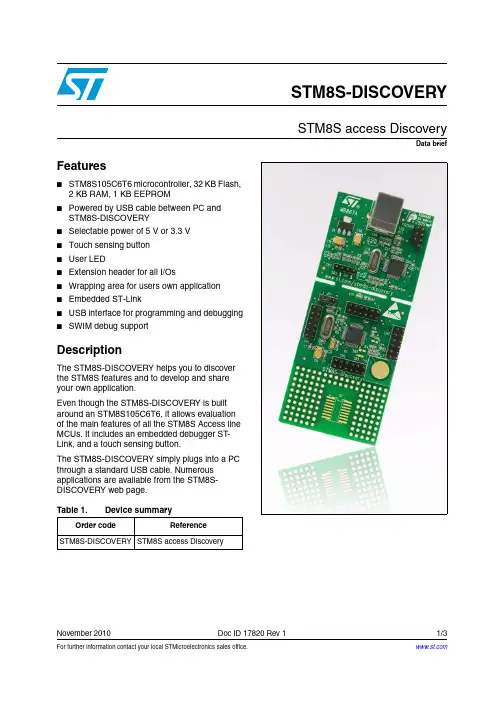
Data briefFor further information contact your local STMicroelectronics sales office.November 2010Doc ID 17820 Rev 11/3STM8S-DISCOVERYSTM8S access DiscoveryFeatures■STM8S105C6T6 microcontroller, 32 KB Flash, 2 KB RAM, 1 KB EEPROM ■Powered by USB cable between PC and STM8S-DISCOVERY ■Selectable power of 5 V or 3.3 V ■Touch sensing button ■User LED ■Extension header for all I/Os ■Wrapping area for users own application ■Embedded ST-Link ■USB interface for programming and debugging ■SWIM debug supportDescriptionThe STM8S-DISCOVERY helps you to discoverthe STM8S features and to develop and shareyour own application.Even though the STM8S-DISCOVERY is builtaround an STM8S105C6T6, it allows evaluationof the main features of all the STM8S Access lineMCUs. It includes an embedded debugger ST -Link, and a touch sensing button.The STM8S-DISCOVERY simply plugs into a PCthrough a standard USB cable. Numerousapplications are available from the STM8S-DISCOVERY web page.Table 1.Device summary Order codeReference STM8S-DISCOVERY STM8S access DiscoverySystem requirements STM8S-DISCOVERY 2/3Doc ID 17820 Rev 11 System requirements●Windows PC (2000, XP , Vista)●USB type A to B cable2 Development toolchain●IAR, Embedded Workbench® for STM8●STMicroelectronics, ST Visual Develop (STVD)3 Demonstration softwareDemonstration software is preloaded in the board's Flash memory. This demonstration usesthe touch sensing feature of the STM8S-Discovery to change the led blinking speed whenthe touch key is pressed. The latest version of the demonstration source code andassociated documentation can be downloaded from /stm8s-discovery.4 Revision historyTable 2.Document revision history DateRevision Changes05-Nov-20101Initial release.STM8S-DISCOVERYPlease Read Carefully:Information in this document is provided solely in connection with ST products. STMicroelectronics NV and its subsidiaries (“ST”) reserve the right to make changes, corrections, modifications or improvements, to this document, and the products and services described herein at any time, without notice.All ST products are sold pursuant to ST’s terms and conditions of sale.Purchasers are solely responsible for the choice, selection and use of the ST products and services described herein, and ST assumes no liability whatsoever relating to the choice, selection or use of the ST products and services described herein.No license, express or implied, by estoppel or otherwise, to any intellectual property rights is granted under this document. If any part of this document refers to any third party products or services it shall not be deemed a license grant by ST for the use of such third party products or services, or any intellectual property contained therein or considered as a warranty covering the use in any manner whatsoever of such third party products or services or any intellectual property contained therein.UNLESS OTHERWISE SET FORTH IN ST’S TERMS AND CONDITIONS OF SALE ST DISCLAIMS ANY EXPRESS OR IMPLIED WARRANTY WITH RESPECT TO THE USE AND/OR SALE OF ST PRODUCTS INCLUDING WITHOUT LIMITATION IMPLIED WARRANTIES OF MERCHANTABILITY, FITNESS FOR A PARTICULAR PURPOSE (AND THEIR EQUIVALENTS UNDER THE LAWS OF ANY JURISDICTION), OR INFRINGEMENT OF ANY PATENT, COPYRIGHT OR OTHER INTELLECTUAL PROPERTY RIGHT. UNLESS EXPRESSLY APPROVED IN WRITING BY AN AUTHORIZED ST REPRESENTATIVE, ST PRODUCTS ARE NOT RECOMMENDED, AUTHORIZED OR WARRANTED FOR USE IN MILITARY, AIR CRAFT, SPACE, LIFE SAVING, OR LIFE SUSTAINING APPLICATIONS, NOR IN PRODUCTS OR SYSTEMS WHERE FAILURE OR MALFUNCTION MAY RESULT IN PERSONAL INJURY, DEATH, OR SEVERE PROPERTY OR ENVIRONMENTAL DAMAGE. ST PRODUCTS WHICH ARE NOT SPECIFIED AS "AUTOMOTIVE GRADE" MAY ONLY BE USED IN AUTOMOTIVE APPLICATIONS AT USER’S OWN RISK.Resale of ST products with provisions different from the statements and/or technical features set forth in this document shall immediately void any warranty granted by ST for the ST product or service described herein and shall not create or extend in any manner whatsoever, any liability of ST.ST and the ST logo are trademarks or registered trademarks of ST in various countries.Information in this document supersedes and replaces all information previously supplied.The ST logo is a registered trademark of STMicroelectronics. All other names are the property of their respective owners.© 2010 STMicroelectronics - All rights reservedSTMicroelectronics group of companiesAustralia - Belgium - Brazil - Canada - China - Czech Republic - Finland - France - Germany - Hong Kong - India - Israel - Italy - Japan - Malaysia - Malta - Morocco - Philippines - Singapore - Spain - Sweden - Switzerland - United Kingdom - United States of AmericaDoc ID 17820 Rev 13/3。
ST单片机STM8S开发入门教程最近ST在国内大力推广他的8位高性价比单片机STM8S系列,感觉性能上还是非常不错的,网上稍微看了点资料,打算有机会还是学习一下,先入门为以后做好技术积累。
好了,长话短说。
手上拿到一套ST最近做活动赠送的三合一学习套件,上面包括STM32F小板、ST LINK小板、STM8S小板,做工很精致,相信很多朋友也收到了。
既然当初去申请了,人家也送了,总得把用起来吧,放着吃灰尘是很可惜的^_^ 。
好,步入正题,刚开始在论坛上逛了一圈,感觉STM8S的资料实在太少,都是官方的应用资料,没有什么入门介绍,连需要安装什么软件都搞不清楚。
偶的电脑光驱坏了,所以也读不出光盘里有什么东西,所以只能到处瞎摸,还是ourdev论坛好,嘿嘿,仔细看了几个帖子,总算明白大概是什么样的开发环境了。
用C语言开发STM8S,需要安装两个软件:1、STVD IDE开发环境;2、COSMIC for STM8 C编译器。
STVD可以到官网下载,下载地址:COSMIC 需要申请LICENSE,比较繁琐,刚好坛子有人传了一个免安装无限制版本的,偶就赶紧下载了,大家可以去下载,仅做为个人学习使用。
下载地址:软件下载后,只需安装STVD。
从上面地址下载的COSMIC不用安装,只要解压到硬盘即可。
后面建立工程的时候设置好路径即可。
下面一步一步开始啦~一、安装好STVD后,桌面上建立了两个快捷图标,ST Visual Develop就是STVD了。
ST Visual Programmer是编程软件,可以配合ST LINK对STM8S进行编程烧录。
二、双击运行ST Visual Develop,启动STVD开发环境。
执行Workspace,在New Workspace 窗口里选择Create workspace and projects,点击“确定”建立工作组和工程三、在Workspace 里输入Workspace名称,由于最终我们要测试一个现成的LED程序,所以偶写了led,随你喜欢了,呵呵。

STM8S MCU family 8-bit microcontroller/mcuSeptember 2008STMicroelectronics’ STM8S family of general-purpose 8-bit Flash microcontrollers offers ideal solutions for industrial and appliance market requirements. An advanced core version combined with a 3-stage pipeline ranks the STM8S microcontroller in the top position for performance. The true embedded EEPROM and the calibrated RC oscillator bring a significant cost effectiveness to the majority of applications. An easy-to-use and intuitive development environment contributes to improving time to market.STM8S: robust and reliableIn addition to performance, comprehensive design specifications and specific peripheral features make the STM8S robust and reliable:n 2 internal RC oscillators with dual independent watchdogsn Clock security system (CSS) to monitor the failure of external clock source n Complementary copy of configuration option bytes and EMS reset n Low emission in accordance with the IEC 61967 standardsn Outstanding robustness performance according to IEC 1000-4-2 and IEC 1000-4-4 standards n High current injection immunity (1 µA leakage current when 4 mA current is injected in adjacent pin)n Dedicated firmware library compliant to Class B of IEC 60335STM8S20x Performance lineUp to 6 KB SRAM2nd UARTSTM8 core @ 24 MHzUARTLIN/Smartcard/IrDA I²C400 kHz multimasterSPI 10 MHz Up to 3 x 16-bit timer8-bit timer 2 x Watchdog (IWDG and WWDG)AWUBeeper 1/2/4 Khz 10-bit ADC Up to 16 channelXTAL16 MHz int.RC osc.128 MHz int.RC osc.SWIM Debug module STM8S10x Access lineSTM8 core @ 16 MHzCAN 2.0BUp to 2 KB SRAMSTM8 core @ 16 MHz Up to 2 KB EEPROMUp to 1 KB EEPROMUp to 128 KB FlashUp to 32 KB FlashSTM8S product linesSTM8 coren 1.6 CPI average n 20 MIPs peak @ 24 MHzn32-bit memory interface n 3-stage pipelinen 16-bit index registers n 20 addressing modesSTM8S MCU familySTM8S portfolioTSSOP20LQFP32LQFP44LQFP64LQFP80LQFP48(*) w/wo EEPROMPerformance linePin count Memory sizeVQFN20, VQFN32 and VQFN48 packages are under qualification Access line (*)Under development© STMicroelectronics - September 2008 - Printed in Italy - All rights reservedThe STMicroelectronics corporate logo is a registered trademark of the STMicroelectronics group of companies.All other names are the property of their respective owners.For more information on ST products and solutions,visit Order code: BRSTM8S0908Device summaryHardware and software development tools 1。
UM0560User manualSTM8 bootloader 1 IntroductionThis document describes the features and operation of the STM8 integrated bootloaderprogram. This code embedded in the system memory of the device (ROM memory allowsmemories, including Flash program, data EEPROM, and RAM, to be written into the deviceusing the standard serial interfaces LINUART/UART/USART, SPI, and CAN.The bootloader code is similar for all STM8 versions. However, even though a peripheralmay be present in a product, the product may not support it (for example the SPI is notsupported in 128 Kbyte devices. In addition, different STM8 device types support differentperipherals (see Table5: Serial interfaces associated with STM8 devices for detailedinformation.For further information on the STM8 family features, pinout, electrical characteristics,mechanical data and ordering information, please refer to the STM8 datasheets.March 2011Doc ID 14798 Rev 41/70Contents UM0560Contents1Introduction . . . . . . . . . . . . . . . . . . . . . . . . . . . . . . . . . . . . . . . . . . . . . . . . 12Bootloader introduction . . . . . . . . . . . . . . . . . . . . . . . . . . . . . . . . . . . . . . 62.1Bootloader activation . . . . . . . . . . . . . . . . . . . . . . . . . . . . . . . . . . . . . . . . . 73Peripheral settings . . . . . . . . . . . . . . . . . . . . . . . . . . . . . . . . . . . . . . . . . 113.1USART/UARTs settings . . . . . . . . . . . . . . . . . . . . . . . . . . . . . . . . . . . . . . 11 3.1.1LINUART/UARTs in “reply” mode settings . . . . . . . . . . . . . . . . . . . . . . . 11 3.2SPI settings . . . . . . . . . . . . . . . . . . . . . . . . . . . . . . . . . . . . . . . . . . . . . . . 123.3CAN settings . . . . . . . . . . . . . . . . . . . . . . . . . . . . . . . . . . . . . . . . . . . . . . 134Bootloader command set . . . . . . . . . . . . . . . . . . . . . . . . . . . . . . . . . . . . 144.1Get command . . . . . . . . . . . . . . . . . . . . . . . . . . . . . . . . . . . . . . . . . . . . . . 154.1.1Get command via USART/LINUART/UART1/ UART2/UART3 . . . . . . . . 15 4.1.2Get command via SPI . . . . . . . . . . . . . . . . . . . . . . . . . . . . . . . . . . . . . . 174.1.3Get command via CAN . . . . . . . . . . . . . . . . . . . . . . . . . . . . . . . . . . . . . 194.2Read memory command . . . . . . . . . . . . . . . . . . . . . . . . . . . . . . . . . . . . . 214.2.1Read memory command via USART/LINUART/UART1/UART2/UART3 214.2.2Read memory command via SPI . . . . . . . . . . . . . . . . . . . . . . . . . . . . . . 234.2.3Read memory command via CAN . . . . . . . . . . . . . . . . . . . . . . . . . . . . . 264.3Erase memory command . . . . . . . . . . . . . . . . . . . . . . . . . . . . . . . . . . . . . 274.3.1Erase memory command via USART/LINUART/UART1/UART2/UART3 . . . . . . . . . . . . . . . . . . . . . . . . . . . . . . . . . . . . . . . . . . . . . . . . . . 284.3.2Erase memory command via SPI . . . . . . . . . . . . . . . . . . . . . . . . . . . . . 314.3.3Erase memory command via CAN . . . . . . . . . . . . . . . . . . . . . . . . . . . . 334.4Write memory command . . . . . . . . . . . . . . . . . . . . . . . . . . . . . . . . . . . . . 354.4.1Write memory command via USART/LINUART/UART1/UART2/UART3 364.4.2Write memory command via SPI . . . . . . . . . . . . . . . . . . . . . . . . . . . . . . 384.4.3Write memory command via CAN . . . . . . . . . . . . . . . . . . . . . . . . . . . . . 414.5Speed command . . . . . . . . . . . . . . . . . . . . . . . . . . . . . . . . . . . . . . . . . . . 434.5.1Speed command via CAN . . . . . . . . . . . . . . . . . . . . . . . . . . . . . . . . . . . 434.6Go command . . . . . . . . . . . . . . . . . . . . . . . . . . . . . . . . . . . . . . . . . . . . . . 454.6.1Go command via USART/LINUART/UART1/UART2/UART3 . . . . . . . . . 454.6.2Go command via SPI . . . . . . . . . . . . . . . . . . . . . . . . . . . . . . . . . . . . . . . 472/70Doc ID 14798 Rev 4UM0560Contents4.6.3Go command via CAN . . . . . . . . . . . . . . . . . . . . . . . . . . . . . . . . . . . . . . 494.7Sector codes . . . . . . . . . . . . . . . . . . . . . . . . . . . . . . . . . . . . . . . . . . . . . . 504.8Software model (STM8A/L/S . . . . . . . . . . . . . . . . . . . . . . . . . . . . . . . . . . 564.8.1RAM erase/write routines . . . . . . . . . . . . . . . . . . . . . . . . . . . . . . . . . . . 575Error management . . . . . . . . . . . . . . . . . . . . . . . . . . . . . . . . . . . . . . . . . 586Programming time . . . . . . . . . . . . . . . . . . . . . . . . . . . . . . . . . . . . . . . . . . 59Appendix A How to upload ROP protected device . . . . . . . . . . . . . . . . . . . . . . . 60A.1Rules for upgrading ROP protected devices. . . . . . . . . . . . . . . . . . . . . . . 60 Appendix B Bootloader entry points . . . . . . . . . . . . . . . . . . . . . . . . . . . . . . . . . . 61Appendix C SPI peripheral timing options. . . . . . . . . . . . . . . . . . . . . . . . . . . . . . 62C.1SPI with busy state checking. . . . . . . . . . . . . . . . . . . . . . . . . . . . . . . . . . . 62C.2Modified erase/write RAM routines. . . . . . . . . . . . . . . . . . . . . . . . . . . . . . 62 Appendix D PC software support . . . . . . . . . . . . . . . . . . . . . . . . . . . . . . . . . . . . . 63Appendix E Bootloader UART limitation . . . . . . . . . . . . . . . . . . . . . . . . . . . . . . . 64E.1Description . . . . . . . . . . . . . . . . . . . . . . . . . . . . . . . . . . . . . . . . . . . . . . . . 64E.1.1UART automatic baudrate calculation. . . . . . . . . . . . . . . . . . . . . . . . . . . 64E.1.2Description of UART limitation . . . . . . . . . . . . . . . . . . . . . . . . . . . . . . . . 64E.2Workaround for UART limitation . . . . . . . . . . . . . . . . . . . . . . . . . . . . . . . . 65 Appendix F Limitations and improvements versus bootloader versions. . . . . 66 Revision history . . . . . . . . . . . . . . . . . . . . . . . . . . . . . . . . . . . . . . . . . . . . . . . . . . . . 68Doc ID 14798 Rev 43/70List of tables UM0560 List of tablesTable 1.STM8 subfamilies featuring abootloader. . . . . . . . . . . . . . . . . . . . . . . . . . . . . . . . . . . . . . . 6 Table 2. STM8 subfamilies without bootloader . . . . . . . . . . . . . . . . . . . . . . . . . . . . . . . . . . . . . . . . . 7 Table3.Bootloader versions for which bootloader activation flowchart isvalid. . . . . . . . . . . . . . . . . 7 Table 4.Initialchecking . . . . . . . . . . . . . . . . . . . . . . . . . . . . . . . . . . . . . . . . . . . . . . . . . . . . . . . . . . 10 Table 5.Serial interfaces associated with STM8devices. . . . . . . . . . . . . . . . . . . . . . . . . . . . . . . . . 11 Table 6.Bootloadercommands . . . . . . . . . . . . . . . . . . . . . . . . . . . . . . . . . . . . . . . . . . . . . . . . . . . . 14 Table 7.Bootloader codes . . . . . . . . . . . . . . . . . . . . . . . . . . . . . . . . . . . . . . . . . . . . . . . . . . . . . . . .14 Table 8.Examples ofdelay . . . . . . . . . . . . . . . . . . . . . . . . . . . . . . . . . . . . . . . . . . . . . . . . . . . . . . . 39 Table9.STM8 sector codes. . . . . . . . . . . . . . . . . . . . . . . . . . . . . . . . . . . . . . . . . . . . . . . . . . . . . . .50 Table 10.Errortable. . . . . . . . . . . . . . . . . . . . . . . . . . . . . . . . . . . . . . . . . . . . . . . . . . . . . . . . . . . . . . 58 Table ART/LINUART/UART1/UART2/UART3 programmingtimes. . . . . . . . . . . . . . . . . . . . . 59 Table 12.SPI programmingtime . . . . . . . . . . . . . . . . . . . . . . . . . . . . . . . . . . . . . . . . . . . . . . . . . . . . 59 Table 13.CAN programming time . . . . . . . . . . . . . . . . . . . . . . . . . . . . . . . . . . . . . . . . . . . . . . . . . . . 59 Table 14.Bootloader entrypoints. . . . . . . . . . . . . . . . . . . . . . . . . . . . . . . . . . . . . . . . . . . . . . . . . . . . 61 Table15.Description of limitation, improvements and addedfeatures . . . . . . . . . . . . . . . . . . . . . . . 66 Table 16.Document revisionhistory . . . . . . . . . . . . . . . . . . . . . . . . . . . . . . . . . . . . . . . . . . . . . . . . . 68 4/70Doc ID 14798 Rev 4UM0560List of figures List of figuresFigure 1.Bootloader activation flowchart . . . . . . . . . . . . . . . . . . . . . . . . . . . . . . . . . . . . . . . . . . . . . . 8 Figure 2.CANframe . . . . . . . . . . . . . . . . . . . . . . . . . . . . . . . . . . . . . . . . . . . . . . . . . . . . . . . . . . . . . 13 Figure 3.Get command via USART/LINUART/UART1/UART2/UART3 - hostside . . . . . . . . . . . . . 15 Figure 4.Get command viaUSART/LINUART/UART1/UART2/UART3 - device side. . . . . . . . . . . . 16 Figure5.Get command via SPI - host side. . . . . . . . . . . . . . . . . . . . . . . . . . . . . . . . . . . . . . . . . . . .17 Figure 6.Get command via SPI - deviceside . . . . . . . . . . . . . . . . . . . . . . . . . . . . . . . . . . . . . . . . . . 18 Figure 7.Get command via CAN - host side. . . . . . . . . . . . . . . . . . . . . . . . . . . . . . . . . . . . . . . . . . . 19 Figure 8.Get command via CAN - device side . . . . . . . . . . . . . . . . . . . . . . . . . . . . . . . . . . . . . . . . . 20 Figure 9.Read memory command via USART/LINUART/UART1/UART2/UART3 - host side. . . . . 21 Figure 10.Read memory command viaUSART/LINUART/UART1/UART2/UART3 - device side . . . 22 Figure 11.Read memory command via SPI - host side . . . . . . . . . . . . . . . . . . . . . . . . . . . . . . . . . . . 23 Figure 12.Read memory command via SPI - deviceside. . . . . . . . . . . . . . . . . . . . . . . . . . . . . . . . . . 25 Figure 13.Read memory command via CAN - host side. . . . . . . . . . . . . . . . . . . . . . . . . . . . . . . . . . . 26 Figure 14.Read memory command via CAN - device side. . . . . . . . . . . . . . . . . . . . . . . . . . . . . . . . . 26 Figure 15.Erase memory command via USART/LINUART/UART1/UART2/UART3 - host side. . . . . 28 Figure 16.Erase memory command viaUSART/LINUART/UART1/UART2/UART3 - device side. . . 30 Figure 17.Erase memory command via SPI - host side . . . . . . . . . . . . . . . . . . . . . . . . . . . . . . . . . . . 31 Figure 18.Erase memory command via SPI - deviceside . . . . . . . . . . . . . . . . . . . . . . . . . . . . . . . . . 32 Figure 19.Erase memory command via CAN - host side . . . . . . . . . . . . . . . . . . . . . . . . . . . . . . . . . . 33 Figure 20.Erase memory command via CAN - device side . . . . . . . . . . . . . . . . . . . . . . . . . . . . . . . . 34 Figure 21.Write memory command via USART/LINUART/UART1/UART2/UART3 - hostside . . . . . 36 Figure 22.Write memory command viaUSART/LINUART/UART1/UART2/UART3 - device side . . . 37 Figure 23.Write memory command via SPI - host side. . . . . . . . . . . . . . . . . . . . . . . . . . . . . . . . . . . . 38 Figure 24.Write memory command via SPI - deviceside. . . . . . . . . . . . . . . . . . . . . . . . . . . . . . . . . . 40 Figure 25.Write memory command via CAN - host side. . . . . . . . . . . . . . . . . . . . . . . . . . . . . . . . . . . 41 Figure 26.Write memory command via CAN - device side. . . . . . . . . . . . . . . . . . . . . . . . . . . . . . . . . 42 Figure 27.Speed command via CAN - hostside. . . . . . . . . . . . . . . . . . . . . . . . . . . . . . . . . . . . . . . . . 43 Figure 28.Speed command via CAN - device side. . . . . . . . . . . . . . . . . . . . . . . . . . . . . . . . . . . . . . . 44 Figure 29.Go command via USART/LINUART/UART1/UART2/UART3 - host side. . . . . . . . . . . . . .45 Figure 30.Go command via USART/LINUART/UART1/UART2/UART3 - device side . . . . . . . . . . . . 46 Figure 31.Go command via SPI - hostside . . . . . . . . . . . . . . . . . . . . . . . . . . . . . . . . . . . . . . . . . . . . 47 Figure 32.Go command via SPI - device side. . . . . . . . . . . . . . . . . . . . . . . . . . . . . . . . . . . . . . . . . . . 48 Figure 33.Go command via CAN - hostside . . . . . . . . . . . . . . . . . . . . . . . . . . . . . . . . . . . . . . . . . . . 49 Figure 34.Go command via CAN - device side. . . . . . . . . . . . . . . . . . . . . . . . . . . . . . . . . . . . . . . . . . 49 Figure35.Delay elimination in modified RAMroutines . . . . . . . . . . . . . . . . . . . . . . . . . . . . . . . . . . . 62 Figure 36."Flash loader demonstrator" software. . . . . . . . . . . . . . . . . . . . . . . . . . . . . . . . . . . . . . . . . 63Doc ID 14798 Rev 45/706/70Doc ID 14798 Rev 42 Bootloader introductionThe main task of the bootloader is to download the application program into the internalmemories through the integrated peripherals (UARTs, SPI, or CAN without using the SWIM protocol and dedicated hardware. Data are provided by any device (host which is capable of sending information through one of the above-mentioned serial interfaces.The bootloader permits downloading of application software into the device memories, including RAM, program and data memory, using standard serial interfaces. It is a complementary solution to programming via the SWIM debugging interface.The bootloader code is stored in the internal boot ROM memory. After a reset, thebootloader code checks whether the program memory is virgin or whether a specific option byte is set allowing code modifications.If these conditions are not fulfilled, the bootloader resumes and the user application is started.In case of a successful check the bootloader is executed.When the bootloader procedure starts, the main tasks are:●Polling all supported serial interfaces to check which peripheral is used●Programming code, data, option bytes and/or vector tables at the address(es received from the host.Each STM8 device embeds a specific bootloader code which is common to a whole group of STM8 devices. The correspondence between STM8 groups and STM8 part numbers is given in Table 1. Group names are used all over this user manual.Table 2 gives the list of STM8 devices without embedded bootloader (no ROM bootloader is implemented inside the microcontroller. When using these devices, youhave to write your own bootloader code and save it in the UBC program area (refer to STM8S and STM8A families reference manual for information on the UBC area.Table 1.STM8 subfamilies featuring a bootloaderSTM8 group STM8 part numbersSTM8A/S-128KSTM8AF52xx, STM8AF6269/8x/Ax, STM8AF51xx, STM8AF6169/7x/8x/9x/Ax,STM8S20xxx STM8A/S-32KSTM8AF622x/4x, STM8AF6266/68, STM8AF612x/4x, STM8AF6166/68,STM8S105xxSTM8L-64k STM8L15xx8, STM8L15xR6, STM8L16xx8STM8L-32KSTM8L15xC4, STM8L15xK4, STM8L15xG4,STM8L15xC6, STM8L15xK6, STM8L15xG6(x = 1 or 2STM8L-8KSTM8L15xC2, STM8L15xK2, STM8L15xG2, STM8L15xC3, STM8L15xK3, STM8L15xG3(x = 1 or 2Doc ID 14798 Rev 47/702.1 Bootloader activationThe STM8 hardware reset vector is located at the beginning of the boot ROM(0x006000,while the other interrupt vectors are in the Flash program memory starting at address 0x008004.The device executes the boot ROM (jumps inside the boot ROM area and after checking certain address locations (see Table 4: Initial checking on page 10, it starts to execute the bootloader or the user code defined by the reset vector (0x008000.The bootloader activation flowchart is described in Figure 1: Bootloader activation flowchart . In previous bootloader versions, a return to the “wait for SYNCHR” state (see dashed line in Figure 1 was performed when the “Flash virgin” test was positive. In newer versions, it has been replaced by a software (SW reset to prevent the customer firmware from remaining in a infinite loop (e.g. due to EMC disturbance. This bootloader modification is referred to as "EMC lockup protection" in T able 15. Table 3 lists the bootloader versions for which the dashed line was replaced by a SW reset.The bootloader version number of a given device is obtained by the “Get command” (see Section 4.1: Get command . The bootloader version is represented by a two-digitbinary-coded decimal (BCD number (with a decimal point between the two digits which is coded into one byte in the “Get command” result. For example, 0x21 version byte is bootloader version 2.1.Table 2.STM8 subfamilies without bootloaderSTM8 group STM8 part numbersSTM8A/S-8K STM8Sx03xx STM8L-8KSTM8L101xxTable 3.Bootloader versions for which bootloader activation flowchart is validSTM8 group Bootloader versionSTM8A/S-128K v2.2STM8A/S-32K v1.3STM8L-64K v1.0STM8L-32K v1.2STM8L-8Kv1.01.See Flow chart description on page9 for explanation of points 1 to 8.2.See Table4: Initial checking.3.Dotted routines are loaded in RAM by the host. They are removed by the go command before jumping to the Flash programmemory to execute an application.8/70Doc ID 14798 Rev 4Flow chart description1.Disable all interrupt sources.2. The host can start the bootloader process according to checks shown in Table4 (inkeeping with the content of the first Flash program memory location (0x008000 and “bootloader enable” option bytes. The host checks the following bootloader startconditions:Condition 1: the host checks if the device memory is empty by inspecting the content of address 0x00 8000 (reset vector. If the content is not equal to 0x82 or 0xAC, thedevice is recognized as being empty and the bootloader remains active and waits for host commands without timeouts.Condition 2: the host checks if the bootloader option bytes (two bytes are set to enable the bootloader or not. The bootloader is enabled with a value of 0x55AA and disabled by all other values (see the device datasheets for the bootloader option byte locations.If the option bytes are enabled, the bootloader remains active and waits for hostcommands with a 1-second timeout. If the host does not send a command within this timeout, the bootloader jumps directly to the application user vector (jump to address0x008000.Condition 3: If the option bytes disable the bootloader (by a value different from0x55AA, the bootloader jumps directly to the application user vector (jump to address 0x00 8000.The above checking process is summarized in T able4.3. When readout protection (ROP is active, the Flash program memory is readoutprotected. In this case, the bootloader stops and the user application starts. If ROP is inactive, the bootloader continues to be executed (see Appendix A: How to upload ROP protected device.4. The CAN peripheral can only be used if an external clock (8 MHz, 16 MHz, or 24 MHzis present. It is initialized at 125 kbps. The UARTs and SPI peripherals do not require an external clock.5. Set the high speed internal RC oscillator (HSI to 16 MHz and initialize the UARTsreceiver pins in input pull-up mode in the GPIO registers. Initialize the SPI in slave mode. Then, wait 4 ms for I/O pin voltage level stabilization. It is recommended that the host waits 10 ms from the STM8 reset before sending the SYNCHR byte/message.This is the time needed for bootloader initialization.Doc ID 14798 Rev 49/7010/70Doc ID 14798 Rev 46.Interface polling: The bootloader polls all peripherals waiting for a synchronizationbyte/message (SYNCHR = 0x7F within a timeout of 1 s. If a timeout occurs, either the Flash program memory is virgin in which case it waits for a synchronizationbyte/message in an infinite loop through a software reset, or the Flash programmemory is not virgin and the bootloader re stores the registers’ reset status and jumps to the memory address given by the reset vector (located at 0x008000. For thebootloader versions listed in Table 3, a software reset is generated after a timeout has elapsed, in case the Flash program memory is empty (this is because it is safer to stay in an infinite loop if there is a hardware chip error.Note:When synchronization fails (the bootloader receives a byte/message different to‘SYNCHR’ = 0x7F two different situations can be distinguished according to the peripheral:With the UART peripherals, a device reset or power-down is necessary beforesynchronization can be tried again. Refer to Appendix E: Bootloader UART limitation With the CAN or SPI peripheral, the user can continue to poll the interfaces until a synchronization or a timeout occurs.7.If the synchronization message is received by the UARTs, the bootloader automatically detects the baud rate, initializes the UART and goes to step 8 below. If thesynchronization message is received by the CAN or SPI, the bootloader goes directly to step 8 below.Note: Once one of the available interfaces receives the synchronization message, all others are disabled.8.Waiting for commands: Commands are checked in an infinite loop and executed. To exit from the bootloader, the host has to send a ‘GO’ command. When this is done, the bootloader removes the EM and WM routines from the RAM memory and jumps to the address selected by the host.Note:To be able to write/erase data in Flash and EEPROM the host must write into RAMexecutable routines for writing and erasing. Those routines (*.s19 files are provided with the bootloader. Host must upload those routines at address 0xA0. See section 4.8.1: RAM erase/write routines for more information.Note:After interface initialization, the ROP bit is checked to avoid non-authorized reading of the Flash program memory and data EEPROM.Table 4.Initial checkingChecksProgram memory byte location [0x008000]Bootloader check option bytes[BL_OPT](11.See device datasheet for the [BL_OPT] location in the option byte area memory map.Actual Flash program memory status-> Flash action1st [0x00 8000] <>(0x82 or 0xAC[BL_OPT] = 0x00XXXX Flash program memory virgin.-> jump to bootloader 2nd[0x00 8000] <>(0x82 or 0xAC[BL_OPT] = 0x0055AA Flash program memory already written, bootloader enabled by option bytes.-> jump to bootloader 3rd[0x00 8000] <>(0x82 or 0xAC[BL_OPT] <> 0x0055AAFlash program memory already written,bootloader disabled by option bytes.-> jump to Flash program memory resetUM0560Peripheral settingsDoc ID 14798 Rev 411/703 Peripheral settingsThis section describes the hardware settings of the STM8 communication peripherals:●UARTs/LINUART ●SPI ●CANNote:During bootloading only one peripheral (first addressed is enabled. All others are disabled.3.1 USART/UARTs settingsThis peripheral supports asynchronous serial communication.The USART/UARTs settings are:●Data frame: 1 start bit, 8 data bit, 1 parity bit set to even, 1 stop bit●Baud rate: The baud rate is automatically detected by the bootloader. When the usersends the synchronization byte, 0x7F , the bootloader automatically detects the baud rate and sets the USART/UARTs to the same baud rate. Maximum baud rate = 1 Mbps (115200 baud for STM8L-64K; minimum baud rate = 4800 bps.To perform the automatic speed detection, the RxD line must be stable in the application board (internal pull-up is enabled on the RxD line by the bootloader.3.1.1 LINUART/UARTs in “reply” mode settingsSettings are:●Data frame: 1 start bit, 8 data bit, no parity bit, 1 stop bit●Baud rate: The baud rate is automatically detected by the bootloader. When the user sends the synchronization byte 0x7F , the bootloader automatically detects the baud rate and sets the UARTs to the same baud rate. Maximum baud rate = 550 kbps (115200 baud for STM8L-64K; minimum baud rate = 4800 bps.To perform automatic speed detection, the RxD line must be stable in the application board (internal pull-up is enabled on the RxD line by the bootloader.Table 5.Serial interfaces associated with STM8 devices (11.The above table reflects only current bootloader versions and device states.STM8 groups Serial interfaceSTM8A-128K USART , LINUART (in “reply” mode, CAN STM8A-32K LINUART, SPISTM8S-128K UART1, UAR T3 (in “reply” mode, CAN STM8S-32K UART2 (in “reply” mode, SPI STM8L-8K UART, SPI STM8L-32K UARTSTM8L-64KUART1, UART2, UART3 (in “reply” mode,SPI1, SPI2Peripheral settings UM056012/70Doc ID 14798 Rev 4Reply modeThe host must reply to all the bytes sent from the bootloader. If TxD and RxD lines share the same physical medium (for example, 1-wire communication, then host replies are not necessary since RxD and TxD pins coincide.3.2 SPI settingsThe SPI settings are:●8 data bit, MSB first●Bit rate: S et by the host which acts as a master●Peripheral set in slave mode with software management of NSS●Data polarity : CPOL = 0 (SCK to 0 when idle, CPHA = 0 (the first clock transition is thefirst data capture edge.Note:1Before sending a ‘token’ byte, th e host has to wait for a delay of a specified period of time. If this period is not quantified, it is equal to 6 µs.2The SPI peripheral is accessible via SPI_SCK, SPI_MOSI and SPI_MISO pins.UM0560Peripheral settingsDoc ID 14798 Rev 413/703.3 CAN settingsTo address additional devices on the same bus, the CAN protocol provides a standardidentifier field (11-bit and an optional extended identifier field (18-bit in the frame. Figure 2 shows the CAN frame that uses the standard identifier only.The CAN settings are as follows:●Standard identifier (not extended●Bit rateBy default, it is 125 kbps. The runtime can be changed via the speed command to achieve a maximum bitrate of 1 Mbps.The transmit settings (from the STM8 to the host are:●Tx mailbox0: On●Tx mailbox1 and Tx mailbox2: Off ●Tx identifier: 0x02●Outgoing messages contain 1 data byteThe receive settings (from the host to the STM8 are:●The synchronization byte, 0x7F , is in the RX identifier and not in the data field●The RX identifier depends on the command (0x00, 0x03, 0x11, 0x21, 0x31, 0x43●Error checking: If the error field (bit [6:4] in the CESR register is different from 000b, the message is discarded and a NACK is sent to the host.●In FIFO overrun condition, the message is discarde d and a NACK is sent to the host.●Incoming messages can contain from 1 to 8 data bytes.Note:The CAN peripheral is accessible via CAN_TX and CAN_RX pins.Bootloader command set UM056014/70Doc ID 14798 Rev 44 Bootloader command setThe commands supported by the bootloader are listed in Table 6 below.Table 7.Bootloader codesWhen the bootloader receives a command via the UARTs, CAN or SPI peripherals, the general protocol is as follows:1.The bootloader sends an ACK byte (0x79 to the host and waits for an address and for a checksum byte, both of which are checked when received.2.When the address is valid and the checksum is correct, the bootloader transmits an ACK byte (0x79, otherwise it transmits a NACK byte (0x1F and aborts the command. The bootloader waits for the number of bytes to be transmitted (N bytes and for its complemented byte (checksum. –If the checksum is correct, it then carries out the command, starting from the received address.–If the checksum is incorrect, it sends a NACK (0x1F byte before aborting the command.Table 6.Bootloader commandsCommandCommand codeCommand descriptionGet 0x00Gets the version and the allowed commands supported bythe current version of the bootloaderRead memory 0x11Reads up to 256 bytes of memory starting from an address specified by the hostErase memory0x43Erases from one to all of the Flash program memory/data EEPROM sectorsWrite memory0x31Writes up to 128 bytes to RAM or the Flash programmemory/data EEPROM starting from an address specified by the hostSpeed 0x03Allows the baud rate for CAN runtime to be changed Go0x21。
UM0970用户手册STM8L-DISCOVERY 简介STM8L-DISCOVERY可以帮助用户探索发现STM8L的超低功耗特性,也可以开发相关的应用。
STM8L-DISCOVERY是基于STM8L152C6T6芯片做的开发板,包括一个嵌入的ST-LINK调试工具接口(ST-LINK调试器/编程器集成在同一块板子上,留有SWIM调试接口)、LCD(24段,4个COM 端)和按键。
图 1STM8L-DISCOVERY板本文仅供参考,请以ST官方文档为准/internet/com/TECHNICAL_RESOURCES/TECHNICAL_LITERATURE/USER_MANUAL/CD00278045.pdf目 录第1章 快速入门 (4)1.1 开始 (4)1.2 系统要求 (4)1.3 开发工具 (5)1.4 演示软件 (5)1.5 订单编码 (5)第2章 特点 (6)第3章 硬件和布局 (7)3.1 STM8L152C6T6微控制器 (11)3.2 嵌入的ST-LINK (13)3.2.1 使用ST-LINK编程/调试板上STM8L (14)3.2.2 使用ST-LINK编程/调试外部STM8L应用 (14)3.3 供电和电源选择 (15)3.4 LED灯 (15)3.5 按键 (16)3.6 内建的IDD测量电路 (16)3.6.1 运行模式 (17)3.6.2 低功耗模式 (17)3.6.3 低功耗模式IDD测量原理 (17)3.6.4 Ibias电流测量步骤 (18)3.7 锡桥 (18)3.8 LCD(24段,4个COM) (19)第4章 扩展连接 (22)第5章 机械制图 (26)第6章 电气原理图 (28)2 - 王志杰(QQ:411238869; MSN:iewangzhijie@)Design a Solution for Future第1章快速入门第1章 快速入门STM8L-DISCOVERY是一个低成本的、易于使用的开发工具,可快速评估和开始一个STM8L超低功耗微控制器的开发。
用户手册STM8S体验系统板STM8S105S4-PKT1 前言STM8S105S4-PKT是ST MCU体验套件中是基于STM8S105S4T6微控制器的,用于评估和体验STM8S功能的电路板。
STM8S105S4T6是精简型的STM8S系列芯片之一,它基于ST公司的先进STM8内核,具有16K字节片上闪存以及一系列丰富的外设接口。
通过ST-LINK、STX-RLINK 等调试工具,可以调试、烧写板载的STM8S105S4T6芯片。
STM8S105S4-PKT电路板提供的接口和外设有USART、ADC、LED灯、蜂鸣器以及触摸感应按键等功能。
图1STM8S105S4-PKT体验套件2 总览2.1 主要特性● 通过套件中的ST-LINK或另外购买的STX-RLINK等调试工具支持免费的STVD开发环境,支持Cosmic STM8的16K免费编译器● 基于STM8S微控制芯片系列芯片之一的STM8S105S4T6高级STM8内核,具有3级流水线的哈佛结构内置16K字节Flash和2K字节RAM内置1024字节EEPROM44个引脚:最多34个通用I/O端口,其中15个大电流端口2个普通16位定时器,1个可产生3路互补PWM输出的高级16位定时器1个带有8位预分频器的8位基本定时器10位ADC,最多有9个ADC输入通道1个带有同步时钟输出的UART ,支持智能卡、红外IrDA和LIN接口1个高达8M位/s的SPI1个支持400K位/s的I2C具有单线接口模块(SWIM)和调试模块(DM)● 可以作为软硬件架构的参考设计● 通过板上的触摸按键,可以体验STM8S的触摸按键方案和性能● 通过板上的蜂鸣器,体验STM8S内置的蜂鸣器驱动单元● 通过板上的扩展区,可以方便地扩展用户自己的外设和体验与STM8S接口操作2.2 板上的资源● 基于STM8内核的STM8S105S4T6芯片● 可选择的8MHz主时钟外部晶振● 三个GPIO驱动的LED灯● 可以输入模拟信号的单通道电位器● 一个复位按键● 一个可由用户定义的按键● 一个RS232(DB9)连接头● 一个SWIM单线调试接口连接头● 三个电容触摸感应式按键● 一个蜂鸣器● 采用PWM+RC滤波的模拟信号输出3 功能、接口及按键图2接口及按键的位置表1连接器、按键及测试点说明标号名称描述CN1 SWIM接口 STM8S程序调试/下载接口CN2, CN3,CN4, CN5扩展接口可用于STM8S芯片引脚功能扩展连接CN7 UART RS-232D型9针连接头J1 电源 9-12V直流输入K1,K2,K3 触摸按键1、2、3电容触摸式按键,分别连接到芯片的PB4、PB5和PB6端口上B1 按键1 芯片复位B2 按键2 用户自定义按键,通过R31连接到芯片的PD7端口上 Ain 模拟输入 连接到电路板上的电位器及芯片的PB3端口上DAC1 模拟输出1 PC1输出PWM 调制信号,通过RC 滤波输出模拟信号,可用PB0引脚采集该信号DAC2 模拟输出2 PC2输出PWM 调制信号,通过RC 滤波输出模拟信号,可用PB1引脚采集该信号DAC3模拟输出3PC3输出PWM 调制信号,通过RC 滤波输出模拟信号,可用PB2引脚采集该信号3.1 SWIM 接口通过该接口可直接访问STM8S 系列芯片的调试模块或对存储器进行编程。
是一个快速启动的STM8S-DISCOVERY评估板,帮助你去发现STM8特性,并且开发和分享你自己的应用程序。
它是基于一个STM8S105 和包括嵌入式调试器,和一个触摸圣链接,传感按钮。
无数应用程序可以从STM8S-Discovery web页面。
特性■STM8S105C6T6单片机,32 KB的Flash,2 KB RAM,eepm 1 KB■采用USB电缆PC和STM8S-DISCOVERY之间■可选择的权力的5 V或3.3 V■触摸感应按钮,壹空间■用户主导,LD1■扩展头所有I / Os■包装区域用户的应用程序■为STM8S嵌入式圣链接■USB接口的编程和调试■游泳调试支持图1。
STM8S-DISCOVERY评估板1快速启动。
32硬件和布局。
42.1 STM8S105C6T6单片机。
62.2圣链接。
82.2.1使用圣链接。
82.2.2使用圣链接在其他应用程序STM8S。
82.3电源和电源的选择。
92.4单触摸感应。
103子板连接。
114电气图纸。
135修订历史。
161快速启动这是非常简单的开始使用STM8S-DISCOVERY,就按照这四个步骤: 1。
STM8S-DISCOVERY连接电脑通过USB电缆。
2。
按壹空间按钮,观察LED LD1闪烁。
3。
按下按钮来改变速度TS1闪烁。
4。
访问/stm8s-discovery并遵循本教程,然后发现其他应用程序。
这个STM8S-DISCOVERY帮助您开发和共享您自己的应用程序。
你可以发现更多的STM8S特性通过下载和执行计划项目在项目列表。
注意:软件代码对应于这个应用程序可用的名义发现在项目列表STM8S-Discovery的web页面。
2硬件和布局设计的STM8S-DISCOVERY在STM8S105C6T6微控制器在一个LQFP48包。
它有两个不同的部分,可能是分开的,STM8S105C6T6 模块和圣链接模块。
图2说明了二者之间的联系STM8S105C6T6及其外围设备(STLINK, 触摸感应按钮,领导和连接器)。
UM0817User ManualSTM8S-DISCOVERYIntroductionThe STM8S-DISCOVERY is a quick start evaluation board which helps you to discover theSTM8 features, and to develop and share your own application. It is based on an STM8S105and includes an embedded debugger, ST-LINK, and a touch sensing button. Numerousapplications are available from the STM8S-Discovery web page.Features■STM8S105C6T6 microcontroller, 32KB Flash, 2KB RAM, 1KB EEPROM■Powered by USB cable between PC and STM8S-DISCOVERY■Selectable power of 5V or 3.3V■Touch Sensing button, TS1■User LED, LD1■Extension header for all I/Os■Wrapping area for users own application■Embedded ST-LINK for STM8S■USB interface for programming and debugging■SWIM debug supportFigure 1.STM8S-DISCOVERY evaluation boardFebruary 2010Doc ID 16361 Rev 21/17Contents UM0817Contents1Quick start . . . . . . . . . . . . . . . . . . . . . . . . . . . . . . . . . . . . . . . . . . . . . . . . . 32Hardware and layout . . . . . . . . . . . . . . . . . . . . . . . . . . . . . . . . . . . . . . . . . 42.1STM8S105C6T6 microcontroller . . . . . . . . . . . . . . . . . . . . . . . . . . . . . . . . 62.2ST-LINK . . . . . . . . . . . . . . . . . . . . . . . . . . . . . . . . . . . . . . . . . . . . . . . . . . . 82.2.1Using the ST-LINK . . . . . . . . . . . . . . . . . . . . . . . . . . . . . . . . . . . . . . . . . . 82.2.2Using the ST-LINK on other STM8S applications . . . . . . . . . . . . . . . . . . 82.3Power supply and power selection . . . . . . . . . . . . . . . . . . . . . . . . . . . . . . . 92.4Single touch sensing . . . . . . . . . . . . . . . . . . . . . . . . . . . . . . . . . . . . . . . . 10 3Daughterboard connection . . . . . . . . . . . . . . . . . . . . . . . . . . . . . . . . . . 11 4Electrical schematics . . . . . . . . . . . . . . . . . . . . . . . . . . . . . . . . . . . . . . . 13 5Revision history . . . . . . . . . . . . . . . . . . . . . . . . . . . . . . . . . . . . . . . . . . . 162/17Doc ID 16361 Rev 2UM0817Quick startDoc ID 16361 Rev 23/171 Quick startIt is very simple to get started using the STM8S-DISCOVERY , just follow these four steps:1.Connect the STM8S-DISCOVERY to a PC with a USB cable.2. Press the TS1 button, and observe LED LD1 blinking.3.Press the TS1 button to change blinking speed.4. Visit /stm8s-discovery and follow the tutorial, then discover otherapplications.The STM8S-DISCOVERY helps you develop and share your own application. Y ou candiscover more of the STM8S features by downloading and executing the proposed programs in the project list.Note:The software code corresponding to this application is available under the name Discover in the project list of the STM8S-Discovery web page.Hardware and layout UM0817 2 Hardware and layoutThe STM8S-DISCOVERY is designed around the STM8S105C6T6 microcontroller in anLQFP48 package. It has two distinct sections that may be separated, the STM8S105C6T6module and the ST-LINK module.Figure2 illustrates the connections between the STM8S105C6T6 and its peripherals (ST-LINK, touch-sensing button, LED and connectors).Figure3 helps you to locate these features on the STM8S-DISCOVERY board, as well asthe potential point of separation (for more details refer to Section2.2.2: Using the ST-LINKon other STM8S applications).Figure 2.Hardware block diagramSTM8S105C6T64/17Doc ID 16361 Rev 2UM0817Hardware and layoutDoc ID 16361 Rev 25/17Figure 3.Top layoutUSB connector ST -LINK JTAGUSB data transfer LEDST -LINK core SWIM connectorS T -L I N K m o d u l ePossible separation pointLED (LD1)Power supply jumper External Osc. (16MHz)STM8S105C6T6T ouch sensing button (TS1)Wrapping areaSO16 footprintS T M 8S 105C 6T 6 m o d u l eHardware and layout UM08176/17Doc ID 16361 Rev 22.1 STM8S105C6T6 microcontrollerFigure 4.STM8S105C6T6 packageThis device provides the following benefits:●Reduced system cost –Integrated true data EEPROM for up to 300K write/erase cycles–High system integration level; internal clock oscillators, brown-out reset, watchdog. ●Performance and robustness –16MHz CPU clock frequency–Up to 38 I/Os on a 48-pin package including 16 high sink outputs –Robust I/O immune against current injection –Independent watchdogs with separate clock source–Flexible clock control, 4 master clocks (HSI, LSI, HSE and external HSE)–Clock security system–A family of products for applications with 2.95 V to 5.5 V operating supply ●Short development cycles –Applications scalability across common family product architecture with compatible pinout, memory map and modular peripherals. –Full documentation and a wide choice of development tools–Standard S/W library for firmware and touch sensing development quick start –Numerous application notes and firmware examples available ●Product longevity –Advanced core and peripherals made in state-of-the-art technology –Low power modes (wait, active-halt, halt)–Auto wake-up timer for active halt –Permanently active, low consumption ●Other features –Nested interrupt controller with 32 interrupts –Up to 37 external interrupts on 6 vectors– 2 x 16-bit general purpose timers; with 2+3 CAPCOM channels (IC, OC or PWM) –Advanced control timer: 16-bit, 4 CAPCOM channels, 3 complementary outputs, dead- time insertion and flexible synchronization –8-bit basic timer with 8-bit prescaler–UART with clock output for synchronous operation, Smartcard, IrDA, LIN –SPI interface up to 8Mbit/s –I2C interface up to 400Kbit/s–Analog-to-digital converter 10-bit, ±1 LSB ADC with up to 10 multiplexed channelsThe STM8S105C6T6 8-bit microcontroller offers:1Kbyte true data EEPROM 32Kbytes of Flash program memory 2Kbytes RAMUM0817Hardware and layout Figure 5.STM8S105 block diagramFor more information see the STM8S105xx datasheet (Doc ID 14771) on the ST website.Doc ID 16361 Rev 27/17Hardware and layout UM08178/17Doc ID 16361 Rev 22.2 ST-LINKThe ST -LINK provides a USB interface for programming and debugging using a single wire interface module (SWIM). The ST -LINK module of the STM8S-DISCOVERY also supplies 5V and 3.3V to the STM8S105C6T6 module.2.2.1 Using the ST-LINKFigure 6.Typical configurationNote:The driver for ST -LINK is installed automatically when the USB is connected.For information about debugging and programming features refer to ST -LINK UM0627, UM0036 STVD and RN0011 STVP . For information about SWIM refer to UM0470.2.2.2 Using the ST-LINK on other STM8S applicationsY ou can connect your ST -LINK to other STM8S applications in 2 ways.●By removing the solder bridges: This way uses the ST -LINK without breaking the PCB. Unsolder the two solder bridges SB1 and SB2 under the SWIM connector.See Figure 7. Y ou can re-solder the two bridges at a later date thus keeping the STM8S-DISCOVERY usable.●By removing it from your board: This way constitutes a good alternative to programming the STM8S devices in other applications. See Figure 8.Note:This ST -LINK only supports the STM8S family. Do not use it with other STM8 families.Figure 7.ST-LINK without breaking the PCBHardware requirements:- USB cable type A to B- Computer with Windows 2000, XP or Vista OSST T oolset (ST Visual Develop and ST Visual Program)Software requirement:which support ST -LINK SWIMRemove SB1 and SB2 solder bridgesUM0817Hardware and layoutDoc ID 16361 Rev 29/17Figure 8.Separated ST-LINK moduleWarning:By removing this module you will lose power supply on the STM8S105C6T6 evaluation board. In consequence, you will not be able to program and use the STM8S105C6T6 board without a SWIM cable and an external power supply. To reconnect your STM8S105C6T6 use connector CNn see Section 3: Daughterboard connection .2.3 Power supply and power selectionThe power supply is provided by a USB connector. Jumper JP1 selects the VDD value (5V or regulated 3.3V) see Figure 9.Figure 9.Power selectionSWIMSTLinkSTM8S105C6 eval boardSTM8S105C6T6VDD = 5VVDD = 3.3VHardware and layout UM081710/17Doc ID 16361 Rev 22.4 Single touch sensingA touch sensing button TS1 is available on the STM8S-DISCOVERY (see Figure 10).Figure 10.Touch sensing schematicTo disable the touch sensing interface and to use PC1, PC2 and PC3 as standard I/O, youneed to unsolder the 2-1 connection and solder 2-3 connection on SB4 and SB3, you also need to unsolder the R2 resistor.RC acquisition principleThe RC acquisition method detects a human touch on key touch sensor (TS1) by measuring the small variation of the touch electrode capacitance. Electrode capacitance is periodically charged and discharged through a fixed resistor (R6).The capacitance value depends on the following parameters: electrode area (A), relative dielectric constant of the insulator (eR), the relative permittivity of air (e0) and the distance between the two electrodes.For more information about touch sensing please refer to AN2927.UM0817Daughterboard connectionDoc ID 16361 Rev 211/173 Daughterboard connectionFour 12-pin male headers CN1, CN2, CN3 and CN4 are connected to the STM8S105C6T6microcontroller. See the following tables for pin assignments.Table 1.CN1 pinoutPin number (Cn1)Pin number (chip)Pin name T y p eMain function Alternate function11NRST IO Reset 22OSCIN/P A1IOPort A133OSCOUT/P A2IO Port A244Vssio_1S I/O ground 55Vss S Digital ground66VCAP S 1.8V regulator capacitor 77Vdd S Digital power supply 88Vddio_1SI/O power supply99P A3IO Port A31010P A4IO Port A41111P A5IO Port A51212P A6IOPort A6Table 2 pinoutPin number (Cn2)Pin number (chip)Pin name T y p eMain function Alternate function125PE5IO Port E5SPI master / slave226PC1/TS1IOPort C1Timer 1 - channel 1 / UART2synchronous clock 327PC2/TS1_load IO Port C2Timer 1 - channel2428PC3IO Port C3Timer 1 - channel 3 529PC4IO Port C4Timer 1 - channel 4 630PC5IO Port C5SPI clock731Vssio_2S I/O ground 832Vddio_2S I/O power supply 933PC6IO Port C6SPI master out / slave in 1034PC7IO Port C7SPI master in / slave out1135PG0IO Port G01236PG1IOPort G1Daughterboard connectionUM081712/17Doc ID 16361 Rev 2Table 3.CN3 pinoutPin number (Cn3)Pin number (chip)Pin name T y p eMain function Alternate function113Vdda S Analog power supply 214Vssa S Analog ground 315PB7IO Port B7Analog input 7416PB6IO Port B6Analog input 6517PB5IO Port B5Analog input 5618PB4IO Port B4Analog input 4719PB3IO Port B3Analog input 3820PB2IO Port B2Analog input 2921PB1IO Port B1Analog input 11022PB0IO Port B0Analog input 01123PE7IO Port E7Analog input 81224PE6IOPort E6Analog input 9(2)Table 4.CN4 pinoutPin number (Cn4)Pin number (chip)Pin name T y p eMain function Alternate function137PE3IO Port E3Timer 1 – break Input 238PE2IO Port E2I2C data 339PE1IO Port E1I2C clock440PE0IO Port E0Configurable clock output 541PD0/LED IO Port D0Timer 3 - channel 2 642PD1/SWIM IO Port D1SWIM data interface 743PD2IO Port D2Timer 3 - channel 1 844PD3IO Port D3Timer 2 - channel 2 945PD4IO Port D4Timer 2 - channel 11046PD5IO Port D5UART2 data transmit 1147PD6IO Port D6UART2 data receive 1248PD7IOPort D7Top level interruptElectrical schematicsElectrical schematics15/17Revision history UM081716/17Doc ID 16361 Rev 25 Revision historyTable 5.Document revision historyDateRevisionChanges05-Oct-20091Initial release.12-Feb-20102Section 2.4: RC acquisition principle modified.UM0817Please Read Carefully:Information in this document is provided solely in connection with ST products. STMicroelectronics NV and its subsidiaries (“ST”) reserve the right to make changes, corrections, modifications or improvements, to this document, and the products and services described herein at any time, without notice.All ST products are sold pursuant to ST’s terms and conditions of sale.Purchasers are solely responsible for the choice, selection and use of the ST products and services described herein, and ST assumes no liability whatsoever relating to the choice, selection or use of the ST products and services described herein.No license, express or implied, by estoppel or otherwise, to any intellectual property rights is granted under this document. If any part of this document refers to any third party products or services it shall not be deemed a license grant by ST for the use of such third party products or services, or any intellectual property contained therein or considered as a warranty covering the use in any manner whatsoever of such third party products or services or any intellectual property contained therein.UNLESS OTHERWISE SET FORTH IN ST’S TERMS AND CONDITIONS OF SALE ST DISCLAIMS ANY EXPRESS OR IMPLIED WARRANTY WITH RESPECT TO THE USE AND/OR SALE OF ST PRODUCTS INCLUDING WITHOUT LIMITATION IMPLIED WARRANTIES OF MERCHANTABILITY, FITNESS FOR A PARTICULAR PURPOSE (AND THEIR EQUIVALENTS UNDER THE LAWS OF ANY JURISDICTION), OR INFRINGEMENT OF ANY PATENT, COPYRIGHT OR OTHER INTELLECTUAL PROPERTY RIGHT. UNLESS EXPRESSLY APPROVED IN WRITING BY AN AUTHORIZED ST REPRESENTATIVE, ST PRODUCTS ARE NOT RECOMMENDED, AUTHORIZED OR WARRANTED FOR USE IN MILITARY, AIR CRAFT, SPACE, LIFE SAVING, OR LIFE SUSTAINING APPLICATIONS, NOR IN PRODUCTS OR SYSTEMS WHERE FAILURE OR MALFUNCTION MAY RESULT IN PERSONAL INJURY, DEATH, OR SEVERE PROPERTY OR ENVIRONMENTAL DAMAGE. ST PRODUCTS WHICH ARE NOT SPECIFIED AS "AUTOMOTIVE GRADE" MAY ONLY BE USED IN AUTOMOTIVE APPLICATIONS AT USER’S OWN RISK.Resale of ST products with provisions different from the statements and/or technical features set forth in this document shall immediately void any warranty granted by ST for the ST product or service described herein and shall not create or extend in any manner whatsoever, any liability of ST.ST and the ST logo are trademarks or registered trademarks of ST in various countries.Information in this document supersedes and replaces all information previously supplied.The ST logo is a registered trademark of STMicroelectronics. All other names are the property of their respective owners.© 2010 STMicroelectronics - All rights reservedSTMicroelectronics group of companiesAustralia - Belgium - Brazil - Canada - China - Czech Republic - Finland - France - Germany - Hong Kong - India - Israel - Italy - Japan - Malaysia - Malta - Morocco - Philippines - Singapore - Spain - Sweden - Switzerland - United Kingdom - United States of AmericaDoc ID 16361 Rev 217/17。