DA14580启动接口和顺序
- 格式:pdf
- 大小:887.99 KB
- 文档页数:15

DA14580最小蓝牙模块MN581A 模块是针对无线智能产品设计的一款超低功耗的,超小体积的蓝牙模块。
基于德国DAILOG超级蓝牙芯片DA14580设计,包含天线部分仅有5.50mm*8.0mm,高度仅有1.7mm 片上集成32 位ARM Cortex M0™处理器国际标准的Blue-tooth® Smart协议栈。
特别适合对体积和高度有特殊需求的智能穿戴式设备。
例如智能手环,蓝牙手表、无线键盘、无线鼠标、平板电脑、手机、笔记本电脑等产品。
可帮助客户快速开发蓝牙4.0产品。
1.1 主要的特点超低功耗最小尺寸内嵌16MHZ32位ARMCortexM0™处理器专用链路层处理器内置aes-128位加密处理器-Time-Programmable(OTP)内存系统SRAM记忆存储器支持多个数字接口:通用I/o、2个UARTs与硬件流控制1MBd、SPI+™接口总线在100kHz,400千赫硬件正交解码能力支持模拟接口设备内置4通道10-bitADC完全集成2.4GHzCMOS收发器单线天线:内置50欧姆天线匹配直接连接2.4G的天线电源电流:传输输出功率-93dBm接收机灵敏度1.2 应用市场智能穿戴式设备蓝牙手表无线键盘无线鼠标平板电脑手机笔记本电脑1.3 管脚定义及尺寸图名称功能输入输出说明GND 接地—VCC模块电源正极2.7V to3.3V—支持聚合物(需降压)、钮扣电池P0_6/TX 模块串口发送端OP0_5/RX 模块串口接收端IP0_3 模块状态切换脚I模块状态切换脚(下降沿唤醒、上升沿睡眠)P0_0 蓝牙数据引脚O蓝牙数据引脚(蓝牙连接\断开\接收数据时都会使此IO 电平变换)VPP,SW_CLK,SWDIO-- 调试软件用VPP,SW_CLK,SWDIO1.5 外围参考设计1.6 模块功耗睡眠模式:2uA唤醒后功耗:500uA连接状态功耗(以1k的发送速率):625uA1.7 模块工作说明本模块为透传模块,在配置完模块的对应I/O 后,应切换下P0_3 的高低电平以保证,模块处于用户所希望的状态(睡眠或者唤醒)。

DA14580蓝牙智能系统级芯片(SoC)推出的号称全球功率最低、体积最小的SmartBond DA14580智能系统级芯片(),与竞争计划相比,该产品可将搭载应用的智能型手机配件,或计算机周边商品的电池巡航时光延伸一倍。
DA14580简介:Dialog推出的号称全球功率最低、体积最小的SmartBond DA14580蓝牙智能系统级芯片(SoC),与竞争计划相比,该产品可将搭载应用的智能型手机配件,或计算机周边商品的电池巡航时光延伸一倍。
该款芯片的设计目的是透过无线方式将键盘、鼠标或遥控器与平板计算机、笔记型计算机或智能电视户相衔接;让消费者能够透过智能型手机和平板计算机上的各种创新应用,与手表、护腕或智能卷标建立衔接,实现如“自我评测”健康和身体情况,和寻觅遗失的钥匙等各种功能。
SmartBond是首款突破4mA无线收发极限的蓝牙智能解决计划,能够让设计人员将产品的电池续航时光延伸一倍,或缩减所需电池的数量和大小。
其独特的低功率架构的无线收发电流仅消耗3.8mA,比市场上其它蓝牙智能解决计划低50%,而且其深度睡眠模式的电流低于600nA。
这表示在一个每秒发送20字节的产品中,一颗 225mAh纽扣电池可以让其持续运作4年5个月;与此相比,前几代蓝牙智能技术仅能维持2年时光。
DA14580拥有一个功率管理区块,内含一个DC-DC转换器以及全部须要的,从而降低对外部组件以及总物料清单的需求。
透过精准地打开和关闭每个芯片块的供电,Dialog能够将功耗降至最低。
SmartBond 的运作可降低至此前所未有的0.9V,从而实现用法一颗碱性电池或镍锰电池就能运作计算机或智能电视周边商品,而过去则需要两颗电池。
这为设计人员放开了通往很多新设计思路的大门,让他们能够开发出超紧密和新尺寸的产品,同时降低系统的总成本。
能源采集技术,如采集到的光能或动能,也可以用于对支持系统运作的可充电电池举行充电。
第1页共5页。

BDF002-如何将产测程序(prod_test)与应用程序放在同一个img文件中--避免生产时需要烧录两次程序的麻烦文档版本:v0.0.1蓝牙生产过程中,对其进行RF性能测试是不可避免的流程,官方在SDK中提供了DA1458x的RF测试工程prod_test,那么问题来了,为了测试,产线上先得烧录一个prod_test程序,测试完毕再烧录最终的应用软件,这样无疑增加了产线的负担,从而令生产成本上升。
那么,能不能一次性解决问题呢?当然是可以的。
这里我们以DA14580为例:当然,需要进行这样的操作,DA14580必须外挂FLASH,且空间必须能放下我们所需要的所有代码。
本文的最终目的是制作一个烧录镜像,此镜像包含了最终的量产程序、prod_test程序以及支持OTA的bootloader,通过一个IO口来配置需要运行的程序,如:P01拉低,则程序进入prod_test程序;P01拉高(浮空),则进入正常工作程序。
我们这里以支持SUOTA的img为基础,在这之前,我们需要一些工具,此工具并非SDK中原版的工具,是经过改良的:其中hex2bin.exe为hex转换为bin文件的工具,此工具SDK中已存在,直接用即可;Mkimage.exe为制作img的工具,基于SDK中对应工程修改而来;Prod_test_580.bin为测试用的prod_test程序,直接用SDK中的工程生成即可;Secondary_bootloader.hex需要根据SDK中对应工程修改。
为了方便大家,以上工具我做了一个下载地址,有需要可直接下载,具体地址见文章最后。
看到这里,镜像文件基础上,在FLASH(EEPROM)的最后增加一个prod_test应用程序,在bootloader启动的时候,通过IO口选择时跳转到fw_x.img还是跳转到prod_text.img。
这样就实现了我们之前提出的功能,一个程序解决程序烧录以及RF测试。

产品概述E104-BT02是一款超高性价比的1mW(0dBm)串口转BLE模块,使用PCB天线。
工作在2.4GHz频段。
模块可使用串口收发蓝牙数据,降低了蓝牙应用的门槛。
E104-BT02模块是基于Dialog公司的DA14580芯片研发,模块集成了透传功能、主从一体,即拿即用。
支持串口指令配置模块参数和功能,广泛应用于穿戴设备、家庭自动化、家庭安防、个人保健、智能家电、配饰与遥控器、汽车、照明、工业互联网等领域,模块具有稳定性高和超低的睡眠功耗,从机模式最低工作电流2uA以下(开启广播功能),可实现纽扣单电池供电。
数据传输稳定高效,从机模式下,支持波特率最大19200bps的数据连传功能,是一款名副其实的数据透传模块。
E104-BT02模块支持BluetoothV4.2标准,简单配置后可与符合蓝牙4.2协议的主机建立蓝牙连接,实现串口数据透传。
模块支持主从角色配置,支持主从模块点对点连接实现数据快速透传功能。
最大限度减少开发者的工作和项目开发时间。
目录产品概述 (3)1.产品特点62.典型应用: (6)3.技术参数74.机械特性85.功能简述95.1.封装95.2.推荐连线图95.3.工作模式95.4.数据有效指示 (10)5.5.角色切换105.6.MAC地址绑定 (10)5.7.串口连传105.8.蓝牙包长配置 (10)5.9.UUID配置115.10.蓝牙嗅探115.11.B EACON数据可切换 (11)5.12.空中配置126.操作指令126.1.模块复位指令 (13)6.2.恢复出厂模式 (13)6.3.串口波特率配置指令 (13)6.4.读串口波特率指令 (13)6.5.串口停止位配置指令 (14)6.6.读串口停止位指令 (14)6.7.串口校验位配置指令 (14)6.8.读串口校验类型 (14)6.9.开启广播指令 (14)6.10.停止广播指令 (14)6.11.查询广播状态 (14)6.12.设置普通广播数据 (15)6.13.设置IB EACON广播数据 (15)6.14.设置固定广播数据 (15)6.15.设备名设置156.16.读设备名156.17.设置厂商名156.18.读厂商名156.19.设置软件版本号 (16)6.20.读软件版本号 (16)6.21.设置硬件版本号 (16)6.22.读硬件版本号 (16)6.23.设置模块SN号 (16)6.24.读模块SN号 (16)6.25.设置S YSTEM ID (16)6.26.查询S YSTEM ID (17)6.27.设置模块编号 (17)6.28.查询模块编号 (17)6.29.设置广播间隙 (17)6.30.读广播间隙176.31.设置最大连接间隙 (17)6.32.读最大连接间隙 (17)6.33.设置最小连接间隙 (18)6.34.读最小连接间隙 (18)6.35.设置连接超时 (18)6.36.读连接超时186.37.断开当前连接 (18)6.38.查询蓝牙连接状态 (18)6.39.查询本地MAC地址 (18)6.40.查询已连接设备MAC地址 (19)6.41.设置绑定连接的MAC地址 (19)6.42.读设定的绑定MAC地址 (19)6.43.关闭MAC地址过滤 (19)6.44.开启模式反馈 (19)6.45.关闭模式反馈 (19)6.46.启动扫描196.47.停止扫描206.48.读扫描状态206.49.设置扫描间隙 (20)6.50.查询扫描间隙 (20)6.51.设置扫描窗口时间 (20)6.52.查询扫描窗口时间 (20)6.53.开启嗅探功能 (20)6.54.关闭嗅探功能 (21)6.55.读取当前RSSI值 (21)6.56.打开128BIT UUID显示 (21)6.57.关闭128BIT UUID显示 (21)6.58.设置服务名UUID (21)6.59.设置RXUUID (21)6.60.设置TXUUID216.61.设置MTU长度 (22)6.62.查询MTU长度 (22)6.63.查询设备角色 (22)6.64.串口唤醒开226.65.串口唤醒关226.66.开启数据输出指示 (22)6.67.关闭数据输出指示 (22)6.68.进入休眠后关闭蓝牙连接 (23)6.69.进入休眠后保持蓝牙连接 (23)6.70.空中配置密码认证 (23)6.71.空中配置密码更新 (23)7.UUID说明 (23)8.快速使用239.生产指导2710.常见问题2811.重要声明2812.关于我们错误!未定义书签。
DA14580学习汇总简介芯片名称:DA14580内核:Cortex-M0 32-bit系统时钟:16MHZ 睡眠时钟:32K (所以要外挂两个晶振)协议栈:不开源,采用Riviera Waves授权协议栈IPRam:42 kB System SRAM(存放运行数据)8 kB RetentionSRAM(低漏电存储器,暂存休眠状态下的运行数据)存储方式:32k的OTP(一次性烧录),要实现反复烧录则需要外挂一个flash或者EEPROM 84 kBROM(存放协议栈)最小系统只需7个元件支持仿真烧录方式:串口烧录(JTAG也可以烧录,烧录到外挂的芯片中)封装:34 pins,40pins, 48 pins功耗:首款突破4mA无线收发电流极限的蓝牙智能解决方案(小米手环可满足30天续航)术语Profile:配置文件(在GATT的基础上进行数据的本地处理)GATT:Generic Attribute Profile 通用的配置文件(负责基础的数据通信)DISS:设备信息服务(显示设备的制造商信息)UUID:全球唯一识别码,如0x2A45位设备序列号的UUID(任意蓝牙都可以通过他获取到设备序列号)。
AES:Advanced Encryption Standard 是DA14580中内置的128 位加密处理器development_guide:开发手册GAP:Generic Access Profile 通用接口配置。
跟蓝牙的advertising相关GTL: Generic Transport Layer 通用传输层。
当工作于外部主控模式时,用来传输主控到DA14580的数据NVDS: Non-Volatile Data Storage 非易失性数据存储器OTP: One Time Programmable (memory) 单次可编程存储器PHY:physical layer物理层LL:Link Layer链路层外挂EEPROMDA14580的芯片是没有flash空间的(其实有个32kb的OTP,但只能烧写一次),也可以使用烧录到内存,但是掉电过后就没有程序了。
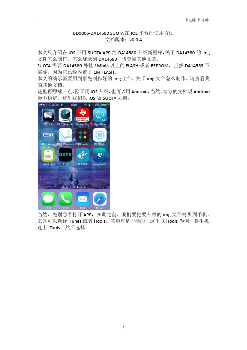
BD0006-DA14580 SUOTA在IOS平台的使用方法文档版本:v0.0.4本文只介绍在IOS下用SUOTA APP给DA14580升级新程序,关于DA14580的img 文件怎么制作,怎么烧录到DA14580,请查阅其他文章。
SUOTA需要DA14580外挂1Mbits以上的FLASH或者EEPROM,当然DA14583不需要,因为它已经内置了1M FLASH。
本文的演示需要用到事先制作好的img文件,关于img文件怎么制作,请查看我的其他文档。
这里再啰嗦一点,除了用IOS升级,也可以用Android,当然,官方的文档说Android 会不稳定。
这里我们以IOS版SUOTA为例:当然,先别急着打开APP,在此之前,我们要把要升级的img文件拷贝到手机。
工具可以选择iTunes或者iTools,其道理是一样的,这里以iTools为例,将手机连上iTools,然后选择:打开SUOTA的文件共享,并选择以下文件夹,将要升级的文件拷贝到该文件夹下,这里我拷贝了3个文件,可以根据自己的需求来拷,反正升级只需要一个:拷贝完毕后关闭iTools,断开手机。
然后打开手机APP,点击搜索,之前请让DA14580工作在广播状态。
不一会儿,就会出现SUOTA02这个设备,这是我们事先烧录好的程序(相关方法请查阅我的其他文档,下文不再重复说明),点击SUOTA02与设备建立连接。
点击Update,选择fw03.img(SUOTA02是fw02.img,所以我们选择新的)。
正常的话会出现以下界面:由于我们用的是FLASH,所以选择SPI,然后根据自己的硬件选择SPI口的配置,关于Image bank,可以选择Oldest-自动选择老的区块覆盖,Bank1-覆盖区块1,Bank2-覆盖区块2,Block size-一般选择默认好了,完毕后点击Send to device。
然后出现以下界面:等待它升级完成,会跳出以下界面:选择reboot,再刷新界面,可以看到更新后的设备—SUOTA03:说明更新成功。
BLE Bluetooth low energy 蓝牙低功耗GAP Generic Access Profile 通用接入规范GATT Generic Attribute Profile 通用属性配置文件GTL Generic Transport Layer 通用传输层HCI Host Controller Interface 主机控制接口RSSI Received Signal Strength Indicator 接受信号强度指示器SDK Software Development Kit 软件开发包URX UART Receive port UART接收端口UTX UART Transmit port UART发送接口(S)RAM (Static) Random Access Memory (静态)随机存取存储器UUID Universal Unique ID 通用唯一IDISR Interrupt Service Routine 中断服务器例程GAPM Generic Access Profile Manager 通用访问配置文件管理器DK Development Kit 开发工具AON Always ON 一直打开API Application Programming Interface 应用程序接口ISR Interrupt Service Routine 中断服务器例程OS Operating System 操作系统RAM Random Access Memory 随机存储器RC16M 16MHz clock generated by internal oscillator 内部振荡器产生16MHZ时钟ROM Read Only Memory 只读存储器WFI Wait For Interrupt instruction 等待中断指令XTAL16M 16MHz crystal 16MHZ晶振DTM Direct Test Mode for Bluetooth Devices 蓝牙设备直接测试模式EUT Equipment Under Test 被测试设备SPOTAR SPotA ReceiverSPOTAI SPotA InitiatorRETRAM Retention RAM 保留内存BLE SIG Bluetooth Low Energy Special Interest GroupMSB Most Significant Byte 最高有效字节LSB List Significant Byte 列出有限字节CLI Command Line Interface 命令行接口GUI Graphical User Interface 图形用户界面HCI Host Controller Interface 主机控制接口XTAL16M 16 MHz Crystal 16 MHz晶振XTAL32K 32 KHz Crystal 32 KHz晶振RC16M 16 MHz RC Oscillator 16MHZ RC振荡器RC32K 32 KHz RC Oscillator 32KHZ RC振荡器Retention RAM Memory that is powered when DA14580 is in Deep sleepRO section Memory section where code (RO) is placedRW section Memory section where global initialized variables are placedScatter file Text file used to specify the memory map of an image to the linkerZI section Memory section where zero initialized variables are placedDMA Direct Memory Access 直接存储器(内存)访问FSM Finite State Machine 有限状态机LDO Low Drop-Out (regulator) 低漏失(校准器) SUOTA Software Update Over The AirDREADY Data ReadyFTDI Quad-Flat No-leadsQFN Quad-Flat No-leadsSRAM Static Random Access MemoryUTX Quad-Flat No-leadsURX Quad-Flat No-leadsURTS Quad-Flat No-leadsUCTS Quad-Flat No-leadsUCTS Quad-Flat No-leadsWLCSP Wafer Level Chip Scale PackagingGAP Generic Access ProfileGTL Generic Transport LayerHCI Host Controller InterfaceNVDS Non-V olatile Data StorageSoC System-on-ChipSPotA Software Patching over the AirCTS Clear To SendRTS Request To SendCLI Command Line InterfaceDUT Device Under TestRF Radio FrequencyIR Infra RedUV Ultra VioletDTM Bluetooth Direct Test ModeWLCSP Wafer Level Chip Scale PackageIRK Identity Resolving KeyLTK Long Term KeyMSB Most Significant BitsMITM Man In The MiddleFOSS Free and Open-Source SoftwareGDB GNU DebuggerIDE Integrated Development EnvironmentKiB Kbyte (1024 bytes)LTO Link-Time OptimisationBTLE Bluetooth Low EnergyPWM Pulse Width ModulationRAM Random Access MemoryROM Read Only MemoryNVIC Nested Vector Interrupt ControllerSysRAM System RAMRetRAM Retention RAMCTS Clear To SendGTL Generic Transport LayerRTS Request To SendIFA Inverted-F AntennaPIFA Planar Inverted-F AntennaRC Remote ControlGTL Generic Transport LayerDISS Device Information Service Server 设备信息服务服务器HAL Hardware Adaptation Layer 硬件适用层。
蓝牙4.1 低功耗BLE 模块YH-001_V1.01(主芯片Dialog_ DA14580)模块概述YH-001_V1.01 是一个蓝牙4.1 单模低功耗(BLE)数传模块,高度集成了蓝牙低功耗射频、协议栈、profile 以及应用程序于系统级芯片DA14580 (内置蓝牙+ARMcortex-M0),它不仅无需外接MCU,而且提供足够的I/O 用于硬件设计和程序开发,非常适合应用于需要超低功耗的系统上。
主要特性1.蓝牙4.1 单模低功耗模块2.完美支持主从模式(Master/Slave)3.集成蓝牙低功耗BLE 协议栈16MHz/32bit ARM Cortex M0,无需要外接MCU4.内置AES-128bit 加密程序5.内置专用链路层处理器6.射频特性TX 功率:-20dBm 至0dBm RX 灵敏度:-93dBm7.通信传输有效距离:30M(无外置功放)8.处理器16MHz 32 位ARM Cortex M0,带有SWD 接口9.内存32kB 的一次性可编程(OTP)闪存42K SRAM 84kB ROM 8kB 保留SRAM10. 工作电压典型值3.0V 建议范围 2.5V-3.3V (支持普通7 号、5 号和纽扣电池供电)11. RF 收发器3V 供电,理想状态TX:3.4mA RX:3.7mA12. 接口4 通道10 位ADC 2 个UART 接口SPI 接口I2C 接口PWM 输出20 通用I/O 接口13. 封装尺寸23.2mm * 17mm * 1.8mm应用领域:1.医疗保健设备2.运动及健康设备3.家庭智能设备4.手机和PC 配件5.工业自动化设备6. 物联网节点设备及网关7. 智能遥控器(含语音识别)8. 手机APP 控制互动玩具9. 手机APP 控制四轴飞行器10.HID 外设,键盘、鼠标……YH-001_V1.01 方框图YH001-V1.01电气特性:绝对最大额定值建议工作条件NOTE1:基于蓝牙芯片RAM 工作特性,要求蓝牙设备冷启动时VDD ≧2.5 V,所以建议模块供电稳定VDD=3V外形尺寸:YH-001_V1.01 的总体尺寸,长23.2 毫米,宽17 毫米,厚1.8 毫米。
BLE-DA14580-Part-9-Da14580 框架----------------------------------------------转载请注明出处------------------------------------BLE-DA14580-Part-8-串⼝透传略..........// DA14580 框架简要分析:以官⽅demo为例,解析经常出现的关键结构,DA14580 中可以创建多个“任务”任务ID如下图,详细查看源码,enum KE_TASK_TYPE{TASK_NONE = 0xFF,TASK_APP = 50 , // Do not Alter.TASK_SAMPLE128 , // Sample128 Task...TASK_MAX = 64, //MAX is 64. Do not exceed.};那么每个ID都会有相应的消息接收函数,查看app.c,app_task.c⽂件,这两个⽂件主要处理蓝⽛底层消息处理定义的Handler部分如下,此时只要知道,当有个消息(⽐如GAPM_CMP_EVT)传送过来,那么接下去就是调⽤gapm_cmp_evt_handler函数。
(那么消息是怎么传过来的?详见下⾯消息传送)EXTERN const struct ke_msg_handler app_default_state[] ={{GAPM_DEVICE_READY_IND, (ke_msg_func_t)gapm_device_ready_ind_handler},{GAPM_CMP_EVT, (ke_msg_func_t)gapm_cmp_evt_handler},{GAPM_DEV_NAME_IND, (ke_msg_func_t)gapm_dev_name_ind_handler},…-…-…-…-}//----------------- 消息发送 -------------------------------------个⼈归纳,可以分为两种类型,⼀种由DA14580内核发送:(我们在源码中查看不到发送的函数,但能找到相应⽂档,查找到相应的⼊⼝函数):参看⽂档RW-BLE-GAP-IS.PDF以及RW-BLE-GAPP-IS.PDF,举例:发送开始⼴播命令给RW-内核,GAPM_START_ADVERTISE_CMD (上述两个⽂档⾃⼰查找下该命令)根据⽂档,会产⽣两种应答:Response: GAPC_CONNECTION_REQ_IND 如果有连接建⽴GAPM_CMP_EVT 当操作完成⼜或者取消那么显⽽易见,当发送完开始⼴播命令时,有连接建⽴时,调⽤上述 app_default_state[] GAPC_CONNECTION_REQ_IND 对应的函数~当操作完成(即设备开始发出⼴播),或者中途⼜发送了停⽌⼴播的命令时,⼀种由我们⾃⼰发送:以bass.c bass_task.c为例在bass_task.c⽂件中定义了如下⼏个状态,每种状态对应⼀个或多个消息函数。
电脑主板与机箱各插口接法详图解解很多朋友会装机,那很简单啊,几块板卡接上就OK了,但是只有主板那密密麻麻的连接线可能让他觉得有点犯晕!好了,直接下面看:一、机箱上我们需要完成的控制按钮开关键、重启键是机箱前面板上不可缺少的按钮,电源工作指示灯、硬盘工作指示灯、前置蜂鸣器需要我们正确的连接。
另外,前置的USB接口、音频接口以及一些高端机箱上带有的IEEE1394接口,也需要我们按照正确的方法与主板进行连接。
机箱前面板上的开关与重启按钮和各种扩展接口首先,我们来介绍一下开关键、重启键、电源工作指示灯、硬盘工作指示灯与前置蜂鸣器的连接方法,请看下图.机箱前面板上的开关、重启按钮与指示灯的连线方法上图为主板说明书中自带的前置控制按钮的连接方法,图中我们可以非常清楚的看到不同插针的连接方法。
其中PLED即机箱前置电源工作指示灯插针,有“+”“-”两个针脚,对应机箱上的PLED接口;IDE_LED即硬盘工作指示灯,同样有“+”“-”两个针脚,对应机箱上的IDE_LED接口;PWRSW为机箱面板上的开关按钮,同样有两个针脚,由于开关键是通过两针短路实现的,因此没有“+”“-”之分,只要将机箱上对应的PWRSW接入正确的插针即可。
RESET是重启按钮,同样没有“+”“-”之分,以短路方式实现。
SPEAKER是前置的蜂鸣器,分为“+”“-”相位;普通的扬声器无论如何接都是可以发生的,但这里比较特殊。
由于“+”相上提供了+5V的电压值,因此我们必须正确安装,以确保蜂鸣器发声。
这是机箱上提供了插头上图为机箱是提供的三种接头。
其中HDDLED是硬盘指示灯,对应主板上的IDE_LED;POWERSW 是电源开关,对应主板上的PWRSW;RESETSW是重启开关,对应主板上的RESET。
除了HDDLED硬盘指示灯有“+”“-”之分外,其它两个没有正负之分,HDDLED硬盘指示灯“+”“-”插反了机箱上的硬盘指示灯不会亮。
当然,为了方便消费者安装,“+”采用了红、棕与蓝进行了标识,而“-”绝一为白色线缆,这一点在任何的机箱当中是通用的,大家可以仔细观察一下。
Application note DA14580 Booting from serialinterfacesAN-B-001AbstractThe DA14580 can boot from external serial devices when the OTP memory is not programmed, to enable development of the application code. At power-up the system enters Development Mode, where the boot code decides which interface to boot from. This document describes the booting sequence for all supported serial interfaces and provides the developer with the necessary information for realising the protocol required for establishing communication between an external device and the DA14580.ContentsContents (2)Figures (3)Tables (3)1 Terms and definitions (4)2 References (4)3 Introduction (5)4 Booting pins (5)5 Booting protocols (6)5.1DA14580 connected to SPI Master (6)5.2DA14580 connected to UART (7)5.3DA14580 connected to SPI Slave (8)5.4DA14580 connected to I2C Slave (9)6 Timing details (11)Revision history (14)FiguresFigure 1: Scan timing for booting from external serial devices (11)Figure 2: Boot timing from SPI Master (11)Figure 3: Boot timing from UART (12)Figure 4: Boot timing from UART: zoomed steps 4 to 6 (12)Figure 5: SPI Slave and I2C boot timing (13)Figure 6: Overview of 5 SPI/I2C boot iterations (13)TablesTable 1: Pin assignment and booting sequence from external devices (5)Table 2: SPI Master boot protocol (6)Table 3: SPI Master data communication (7)Table 4: UART baud rates on different pins while booting (7)Table 5: UART boot protocol (7)Table 6: SysRAM word alignment (8)Table 7: SPI Slave boot protocol (8)Table 8: SPI read and dummy byte cases (9)Table 9: I2C boot protocol (9)1 Terms and definitionsOTP One Time Programmable (memory) SW SoftwareURX UART Receive portUTX UART Transmit port2 References1. DA14580, Datasheet Dialog Semiconductor3 IntroductionThe DA14580 operates in two modes, namely the ‘Normal Mode’ and the ‘Development/Calibration Mode’ hereafter addressed as ‘DevMode’. The decision which mode the chip enters after power-up, is taken by the boot code residing in the ROM. A complete flow chart of the booting code is illustrated in the datasheet of the DA14580.DevMode will be entered when the OTP header contains a value zero at the first two addresses, when read by the CPU. This implies that the OTP is not programmed and the DA14580 should switch to the DevMode, so that users get access to download code from external devices into the internal SRAM (SysRAM). However, when the OTP contains specific values (magic numbers) in these locations the DA14580 will enter Normal Mode and proceed with mirroring of the OTP contents into the SysRAM in the booting sequence, as described in the datasheet.To allow for maximum flexibility, a predefined number of pins are examined and utilized at boot time to communicate with external devices using the three serial interfaces available on chip: UART, SPI and I2C. SPI and I2C can be masters on the DA14580 side expecting to communicate with an external slave device and SPI can also be slave expecting to communicate with an external master.4 Booting pinsDuring booting, port P0 is used to check for the presence of external devices. The assignment of the pins as well as the sequence of the interface activation by the boot code is presented in Table 1 below.Table 1: Pin assignment and booting sequence from external devicesThe mapping of the serial interface to each pin is shown in Table 1. Each interface column is preceded by a ‘Step’ column, which corresponds to the seq uence step in the booting procedure. The first step of the boot code is to configure the DA14580’s SPI controller to Slave mode (try to boot from an external SPI Master device) and assign the SPI’s SCK to P0_0, CS to P0_3, MOSI to P0_5 and MISO to P0_6.If nothing is found to be connected on these pins (the protocol is described in section 3.0), then the boot code continues with the second step which looks for an external SPI master at P0_0, P0_1,P0_2 and P0_3.The booting sequence is finished at step 11, when no response is received to P0_6 (SCL) and P0_7 (SDA) and starts all over again from step 7 (SPI Master and UART will not be activated again).Steps 7 to 11 are executed a total of 5 times. If no successful communication has been established by then, the DA14580 boot code will end in an endless (while) loop with the Serial Wire interface (JTAG) activated.5 Booting protocols5.1DA14580 connected to SPI MasterThe boot code initially configures the DA14580 SPI controller with the following parameters:●8 bit mode●Slave role●Mode 0: SPI clock is initially expected to be low and SPI phase is zero.The protocol required for establishing a successful communication and downloading the SW into the SysRAM is depicted in Table 2.Table 2: SPI Master boot protocolThe external SPI master device starts by sending the Preamble bytes (0x70 and 0x50) followed by a zero byte. The DA14580 will confirm the reception of the Preamble with 0x02 (Acknowledged) or0x20 (Not Acknowledged) in case something went wrong. Bytes 3 and 4 define the length of the payload to follow. The least significant byte is sent first. The length is a number which represents the amount of data in 32-bit words.Next, the SPI master must send the calculated CRC of the payload . The CRC is calculated by XORing every successive byte with the previous value. Initial CRC value is 0xFF.Byte 6 defines the mode of operation directed by the SPI master (8, 16 or 32-bit modes) while the DA14580 SPI slave answers with ACK/NACK regarding the reception of the length bytes. The mode is encoded as follows:●0x00 = 8-bit mode●0x01 = 16-bit mode●0x02 = 32-bit mode●0x03 = ReservedByte 8 is the last control byte, where DA14580 replies with ACK/NACK regarding the reception of the CRC and the mode, while the external SPI master starts sending the first byte of the payload (least significant byte of the first word).The data section is presented in Table 3, taking into consideration the instructed mode. The stream of data is followed by 2 extra empty slots to provide the required time to the DA14580 SPI controller to compute the CRC and answer with ACK/NACK.Upon completion of the SPI master process, all related pads are set to input and pulled down. Table 3: SPI Master data communicationDA14580 connected to UART5.2The boot code enters this mode configuring the UART controller with different baud rate parameters depending on the pin mapping as shown in Table 4. Table 4: UART baud rates on different pins while bootingThe rest of the UART parameters are common for all pin mappings, i.e.:● Bits: 8 ● No parityThe protocol required for establishing a successful communication and downloading the SW into the SysRAM is shown in Table 5. Table 5: UART boot protocolThe protocol starts with the DA14580 UART TX pin transmitting 0x02 (Start TX, STX). The external device is expected to answer with a 0x01 (Start of Header, SOH) byte followed by 2 more bytes (LEN_LSB, LEN_MSB) which define the length of the code to be downloaded (first byte is the least significant, second the most significant). The DA14580 answers with 0x06 (ACK) if 3 bytes have been received and SOH has been identified or with 0x15 (NACK) if anything went wrong.At this point the connection has been successfully established and the SW code will start being downloaded. The next N bytes are received and placed into the SysRAM, starting at address0x20000000 as shown in Table 6.Table 6: SysRAM word alignmentFollowing the completion of the required code bytes, the boot code will calculate the CRC and send it over the URX. The booting sequence ends when reading the value 0x06 (ACK) at the URX line. CRC is calculated by XORing every successive byte with the previous value. Initial CRC value is 0x00.During the final step of the boot code, the SYS_CTRL_REG register is programmed to:1. Remap to SysRAM (SYS_CTRL_REG[REMAP_ADR0] = 10).2. Apply a SW reset, so the system starts executing code at the remapped address(SYS_CTRL_REG[SW_RESET] = 10).DA14580 connected to SPI Slave5.3The boot code configures the SPI with the following parameters:●8 bit mode●Master role●Mode 3: SPI clock is initially high and SPI phase is shifted by 90 degrees.●The SPI clock frequency is set at 2 MHz.The protocol required for establishing a successful communication and downloading the SW into the SysRAM is shown in the following table:Table 7: SPI Slave boot protocolThe sequence as described in Table 7 is repeated for four different cases regarding the Read command and the Dummy byte parameters, as indicated in Table 8.Table 8: SPI read and dummy byte casesAs soon as the length has been received (2 bytes), the actual downloading of the code into the SysRAM starts. The start address is the base address of the SysRAM. The byte alignment is according to Table 6.During the final step of the boot code a SW reset is given and the system starts executing the downloaded code5.4DA14580 connected to I2C SlaveThe boot code initializes the I2C controller in master mode with the following parameters:●I2C slave address = 0x50 (7-bit address)●I2C speed to standard mode (100 kbit/s)The boot code initially scans to find an I2C slave device at addresses 0x50 up to 0x57. Following a successful slave address identification, a specific protocol is executed for downloading the SW into the SysRAM as shown in Table 9. If unsuccessful, a timeout is programmed to expire after 20 ms to get the chip out of the I2C booting mode into the next one.Table 9: I2C boot protocolThe boot code will calculate the CRC by XORing every successive byte with the previous value. Initial CRC value is 0x00. The CRC is calculated on multiples of 32 bytes. Padding with zeros is required when the payload size is not a multiple of 32 bytes.During the final step of the boot code a SW reset is given and the system starts executing the downloaded code. During the final step of the boot code a SW reset is given and the system starts executing the downloaded code6 Timing detailsThe time required for the execution of the BootROM code which checks and enables booting from an external serial device is 146 ms. This is illustrated in Figure 1 which displays the power-up sequence of the DA14580 and pins P0_0 to P0_7, which are involved in the 11 steps as explained in Table 1. Note that no actual device is connected so that the whole sequence is executed up to the last step.Figure 1: Scan timing for booting from external serial devicesThe first 2 booting steps turn the pins into inputs, thus expecting an external SPI master device to provide clock and data. This starts 103 ms after the actual power-up of the chip (as illustrated in Figure 2), which is required for internal settling and executing the initial BootROM instructions up to the point of getting into the DevMode.Figure 2: Boot timing from SPI MasterThe next serial interface to be examined for a potential booting sequence is the UART. This spans over booting steps 3 to 6, where the DA14580 is transmitting on the TX line and waits for an answer on its RX line. The whole sequence time may vary from 2 ms up to 240 ms, depending on whether the RX line is high or low.When RX is high, it is acknowledged to be a valid UART state and thus the DA14580 will wait for an answer until a timeout of 208 µs expires. This is displayed in Figure 3 in step 3: P0_0 is the TX signal while P0_1 is the RX which is high during transmission. This triggers the DA14580 to wait for the timer expiration after 208 µs, concluding that there is indeed no external device mounted on these pins and thus it should move to the next step.In the cases of steps 4 to 6 the RX line is low, so the timer is not triggered and the DA14580 just continues on the next step without timer expiration.Figure 3: Boot timing from UARTA better overview of the booting from UART sequence and timing is given in Figure 4, where steps 4 to 6 are zoomed in. Note that the baud rate is different for each step with steps 3 and 5 expecting communication at 57.6 kbit/s, while steps 4 and 6 use 115.2 kbit/s and 9.6 kbit/s respectively.Figure 4: Boot timing from UART: zoomed steps 4 to 6Following the UART booting, the DA14580 searches for an external SPI slave device, as explained in step 7. The clock output (at P0_0) of the DA14580 is toggling at 2 MHz while the whole process takes 640 ms as displayed in Figure 5. Note here that booting from an external SPI slave is repeated 4 times before moving to the next step.Figure 5 also shows the I2C booting process. It consists of 4 different steps that run the SCL (clock) line of the I2C at 100 kHz and require 1 ms for identifying that no external device is connected on these pins.Figure 5: SPI Slave and I2C boot timingThe steps of Figure 5 are repeated up to 5 times when no device is successfully identified on any ofthe pins or interfaces. Each iteration lasts 4.8 ms. The timing overview is presented in Figure 6.Figure 6: Overview of 5 SPI/I2C boot iterationsRevision historyStatus definitionsDisclaimerInformation in this document is believed to be accurate and reliable. However, Dialog Semiconductor does not give any representations or warranties, expressed or implied, as to the accuracy or completeness of such information. Dialog Semiconductor furthermore takes no responsibility whatsoever for the content in this document if provided by any information source outside of Dialog Semiconductor.Dialog Semiconductor reserves the right to change without notice the information published in this document, including without limitation the specification and the design of the related semiconductor products, software and applications.Applications, software, and semiconductor products described in this document are for illustrative purposes only. Dialog Semiconductor makes no representation or warranty that such applications, software and semiconductor products will be suitable for the specified use without further testing or modification. Unless otherwise agreed in writing, such testing or modification is the sole responsibility of the customer and Dialog Semiconductor excludes all liability in this respect. Customer notes that nothing in this document may be construed as a license for customer to use the Dialog Semiconductor products, software and applications referred to in this document. Such license must be separately sought by customer with Dialog Semiconductor.All use of Dialog Semiconductor products, software and applications referred to in this document are subject to Dialog Semiconductor’s Standard Terms and Conditions of Sale, unless otherwise stated.© Dialog Semiconductor GmbH. All rights reserved.RoHS ComplianceDialog Semiconductor complies to European Directive 2001/95/EC and from 2 January 2013 onwards to European Directive 2011/65/EU concerning Restriction of Hazardous Substances (RoHS/RoHS2).Dialog Semiconductor’s statement on RoHS can be found on the customer portal https:///. RoHS certificates from our suppliers are available on request.Contacting Dialog SemiconductorGermany Headquarters Dialog Semiconductor GmbH Phone: +49 7021 805-0United KingdomDialog Semiconductor (UK) Ltd Phone: +44 1793 757700The NetherlandsDialog Semiconductor B.V. Phone: +31 73 640 8822 North AmericaDialog Semiconductor Inc.Phone: +1 408 845 8500JapanDialog Semiconductor K. K.Phone: +81 3 5425 4567TaiwanDialog Semiconductor TaiwanPhone: +886 281 786 222SingaporeDialog Semiconductor SingaporePhone: +65 64 849929ChinaDialog Semiconductor ChinaPhone: +86 21 5178 2561KoreaDialog Semiconductor KoreaPhone: +82 2 3469 8291Email: Web site:。