SV1-D4212 信步主板说明书
- 格式:pdf
- 大小:1.48 MB
- 文档页数:8

VSC8221User Guide VSC8221 Evaluation BoardContents1Revision History (1)1.1Revision 1.0 (1)2Introduction (2)3General Description (3)3.1Hardware Features (3)3.1.1Power Connections (3)3.1.2Copper Port RJ45 Connections (3)3.1.3SFP or SMA SGMII MAC Interface (3)3.1.4Switches (3)3.1.5Taitien 25 MHz Crystal (3)3.1.6External RefClk Option (4)3.1.7Silabs Microcontroller (4)3.1.8EEPROM Option (4)3.1.9CMODE Pins (4)3.1.10CLOCKOUT SMA (4)3.2Software Requirements (4)4Quick Start (5)4.1Board Configuration (5)4.1.1Clock and Reset (5)4.1.2Power Up (5)4.2GUI and Driver Installation (5)4.3Using the GUI (6)4.4Test Cases (7)4.4.1CAT5 to 802.3z Serdes with Clause 37 AutoNeg Detection (7)4.4.2CAT5 to SGMII with Modified Clause 37 AutoNeg Disabled (8)4.5Useful Registers (8)4.5.1Ethernet Packet Generator (8)4.5.2Far-End Loopback (8)4.5.3Near-End Loopback (8)5Additional Information (9)1Revision HistoryThe revision history describes the changes that were implemented in the document. The changes arelisted by revision, starting with the most current publication.1.1Revision 1.0Revision 1.0 was the first release of this document. It was published in December 2013.2IntroductionThe VSC8221 device is a low-power, Gigabit Ethernet transceiver suited for Ethernet Switches with SGMII/SerDes MAC interfaces, Media Converter applications, and SFP/GBIC modules. The VSC8221 device alsoincludes Vitesse’s VeriPHY Cable Diagnostics feature.This document describes the operation of the VSC8221 Evaluation Board (VSC8221EV). The Quick Startsection describes how to install and run the graphical user interface (GUI) to fully control the evaluationboard.Figure 1 • VSC8221EVThe following reference documents provide additional information about the operation of the VSC8221evaluation board.VSC8221 DatasheetVSC8221 Evaluation Board GUIVSC8221 Evaluation Board Schematics3General DescriptionThe VSC8221EV provides the user a way to evaluate the VSC8221 device in multiple configurations. OneRJ-45 connector is provided for the copper media interface. The MAC interface is provided via SMAconnectors or alternatively through an SFP connector.The VSC8221’s internal registers are accessed via the MDIO bus from an external microcontroller drivenby an external PC via USB. The accompanying GUI enables the user to read and write the deviceregisters. Alternatively, the VSC8211EV also has the capability to configure the VSC8221 through anEEPROM or Rabbit microcontroller (not-provided).The evaluation board has the option to use VSC8221’s internal on-chip oscillator by connecting a 25MHzcrystal to XTAL1 and XTAL2 or an external reference clock signal through the REFCLK SMA (J11).3.1Hardware Features3.1.1Power ConnectionsFor convenience, the evaluation board runs off a single +5VDC power supply. On board DC-DCconvertors create the +3.3VDC rail for the board and optional +1.2VDC rail. Power is supplied to theupper right corner of the board. Power can be applied either to the 5.5 x 2.1 mm barrel connector (J20)or the banana receptacles (J21 and J15). The slide switch (SW-4) selects between the external (on-board) and internal (on-chip) regulator option. J22 is an optional monitor point for the 1.2 V rail. Whenpowered by a bench top supply the board may draw up to 3 A maximum, module included.3.1.2Copper Port RJ45 ConnectionsThe RJ45 copper media PHY port (J1) uses a generic RJ45 jack with a discrete Pulse H5008 magnetictransformer.3.1.3SFP or SMA SGMII MAC InterfaceThe default MAC interface is provided through an SFP port connector. When using the SFP port, theSigDet polarity must be swapped in the VSC8221. See register 19E.0. Note that the transmit disablesignals (TXDIS) are connected to ground, thus the laser is always turned on.An optional MAC interface through SMA connectors may be enabled by removal and re-soldering the ACcoupling caps (C7–C10) from horizontal to vertical position.3.1.4SwitchesThere are two switches on the board:SW4 to select between utilizing a +1.2V internal regulator or external regulator. The default optionfor the board is to use the external regulator.SW2 allows the user to select the mode of the EECLK/PLLMODE pin. In the on position a logic highvoltage (pull-up resistor) configures the device for a 125MHz reference clock while a logic lowvoltage (pull-down resistor) selects a 25MHz reference clock option. This is a momentary ON switchwhich requires the user to hold it in the on position for 3 seconds during board power up or devicereset.3.1.5Taitien 25 MHz CrystalThe evaluation board is shipped configured to use the VSC8221’s internal on-chip oscillator. The jumperon J12 should be installed in the XTAL (left) position, and the jumper on J24 should be installed in thePLL enable or VCC (right) position.Note: Review the required action for SW2 mentioned above.1. 1.2.3.1.6External RefClk OptionThe user may choose to provide an external PHY REFCLK via the SMA connector (J11). The user must configure the device by installing a jumper on J24 in the PLL disable or ground (left) position and installing a jumper on J12 in the SMA (right) position.3.1.7Silabs MicrocontrollerA Silabs F340 microcontroller is included to facilitate a software interface to the registers on the VSC8221through a USB port.3.1.8EEPROM OptionThe user may choose to configure theVSC8221 via an EEPROM load. In order to program the EEPROM properly, pull-up or pull-down resistors must be configured for either R7 – R9 or R15 – R17. See Section 19 of the datasheet regarding to EEPROM programming requirement.3.1.9CMODE PinsOn the lower center of the board, there is an option to change the CMODE pin pull-up or pull-down resistors, R6, R12 – R14, and R18 – R21. See Section 18 of the datasheet for the detail on how toprogram the desired operating condition parameters through the CMODE configuration bits and how to choose the value of each CMODE pull-up or pull-down resistor.3.1.10CLOCKOUT SMAThe user should observe a 125MHz output clock through this SMA if the internal PHY PLL is operating properly.3.2Software RequirementsThe VSC8221 GUI can be loaded on to any PC or laptop that complies with the following requirements:The PC must run a recent version of MS-Windows. According to the Microsoft website, the following operating systems can run .NET based applications:Windows 2000Windows XP Windows Vista Windows-7Note: The GUI may be slower when run on Windows 2000 operating system.Hardware requirements must be considered when deploying/installing .NET applications. The minimum hardware requirement for a system running a .NET application is a Pentium 90MHz with 32 MB of RAM. For best performance, a newer system is recommended along with a minimum of 1 GB of RAM.If the .NET Framework 2.0 is not already installed, it may be obtained from the following link: /downloads/details.aspx?FamilyID=0856EACB-4362-4B0D-8EDD-AAB15C5E04F5&displaylang=en4Quick Start4.1Board ConfigurationPrior to powering the board, ensure that the jumpers and switches are in the following positions.Table 1 • Switch and Jumper ConfigurationSwitch/Jumper PositionJ19 (MDC)Jumper installed connecting F340 MDC to DUT MDCJ19 (MDIO)Jumper installed connecting F340 MDIO to DUT MDIOJ14 (TRSTB)Jumper installed connecting to GND. This is not requiredwhen R48 is installed.J12 (XTAL1/REFCLK)Jumper installed connecting center pin to XTAL.J24 (PLL ENABLE/DISABLE)Jumper installed connecting center pin to PLL ENABLE.SW2Hold in the left position during power-up and reset.SW4Slide to the left to use the on-chip regulator.4.1.1Clock and ResetPower must be applied and the clock (either 25 MHz or 125 MHz) must be active at the correctfrequency for the prescribed period of time in the datasheet before the RESETB pin is released.PLLMODE and OSCDISB pins are sampled during the device power-up or on assertion of RESETB pin.The board will be shipped configured for use of the 25 MHz crystal thus OSCDISB must be pulled up andPLLMODE must be pulled down during power-up or assertion of RESETB by setting J24 to the PLL enableposition and holding SW-2 in the 25 MHz position upon power-up.4.1.2Power UpProvide +5VDC to the board by plugging in the power cable (included in the kit) to J20. Two green LEDsshould illuminate: D12 on the left side of the board indicating +3.3VDC present and D11 on the right sideof the board indicating +1.2VDC present.4.2GUI and Driver InstallationDownload the VSC8221EV GUI from Vitesse’s website onto a PC that has a USB port. Install the GUI bylaunching the setup.exe file. Once installed, connect the USB cable between the USB port of the PC andthe USB connector (J16) on the evaluation board. Ensure the MDIO and MDC jumpers are properlyplaced from DUT to F340 on J23 to establish the connection between the VSC8221’s SMI pins and theSiLab F340.USB communication is assisted by the Silabs USBXpress® drive. If not present on the PC, the user willneed to download the USBXpress Development Kit from the Silicon Labs website (URL: http://www./products/mcu/Pages/USBXpress.aspx). Follow the installation directions after downloading the development kit.To ensure the USBXpress driver is installed and properly recognizing the evaluation board, go to ControlPanel and click on System>Hardware>Device Manager, and inspect the Universal Serial Bus controllerslisted to see if “USBXpress Device” appears. The following figure shows that the PC recognizes that aUSBXpress Device is connected.Figure 2 • USBXpress as Seen from the Device Manager Window4.3Using the GUILaunch the GUI either by clicking on the Desktop shortcut or clicking on the “Start – Programs – VitesseSemiconductor Corp - VSC8221_Evaluation_System” icons. The initial window will detect the attachedUSB devices automatically. The following figure shows a typical EVB Connection window.Figure 3 • Connection WindowThe EVB serial number should appear. If not, click on “Scan For USB Devices.” Select that EVB serialnumber then click “Launch GUI”. The Register List window will appear as shown in the following figure.1. a. b. c. d.Figure 4 • Register List WindowVerify that the device is up and running by reading MII Register 0. It should read back 0x1040. Reading back “0000” or “FFFF” (all 0’s or all 1’s) indicates a problem.To read or write the extended MII registers click on the ExtMII tab.An initialization script may be used to configure multiple VSC8221 registers. The initialization script is simply a text file which contains a list of registers to be written. Select the Device item on the top pull down menu area and click on Load-All-Registers option. A pop-up window will appear. Navigate to and select the desired script to be loaded.As per Section 31.1 of the datasheet, there are a number of internal registers that must be changed from their default value during device initialization. Use this method to initialize the device by loading “vsc8221_workaround31_1.txt” included in the GUI package under the Script/ directory. GUI Setup4.4Test Cases4.4.1CAT5 to 802.3z Serdes with Clause 37 AutoNeg DetectionAfter power-up or reset, the VSC8221 will operate at CAT5 to 802.3z Serdes with clause 37 Auto Negotiation Detection mode. An SFP loopback module enables MAC side SGMII loopback. 1G Ethernet received by the VSC8221 RJ-45 port is routed through the VSC8221 and looped back via SGMII through the SFP Electrical Loopback module.Set up the copper Ethernet traffic source (e.g., IXIA or Smartbits).Connect an Ethernet cable to an RJ-45.Plug in a SFP loopback module.Monitor the link-up bit in MII Register 1, bit 2 (MII 1.2), read twice to update. Traffic should now be flowing.1. 2. 3. 4. 5. 6. 4.4.2CAT5 to SGMII with Modified Clause 37 AutoNeg DisabledTo configure the device for Clause 37 Auto-negotiation disabled, perform these steps:Set up the copper Ethernet traffic source (e.g., IXIA or Smartbits).Connect an Ethernet cable to an RJ-45.Plug in a SFP loopback module.Write 0xBA20 to “MII Register” (Port 0) Reg 23 (Extended PHY Control #1).Write 0x9040 to “MII Register” (Port 0) Reg 0 (SW Reset for PHY Control setting to take effect).Monitor the link-up bit in MII Register 1, bit 2 (MII 1.2), read twice to update. Traffic should now be flowing.4.5Useful Registers4.5.1Ethernet Packet GeneratorExtMII 29E is the Ethernet Packet Generator register. Refer to datasheet for configuration options.A bad-CRC counter is in ExtMII 23.7:0. This counter will be saturate at 0xFF and is cleared when read.4.5.2Far-End LoopbackWhen MII Register 23 bit 3 is set to 1, it forces incoming data from a link partner on the media side to be retransmitted back to the link partner on the media interface.4.5.3Near-End LoopbackWhen MII Register 0 bit 14 is set to 1, the transmit data (TDP/TDN) on the MAC side is looped back onto the receive data (RDP/RDN pins) to the MAC.5Additional InformationFor any additional information or questions regarding the device(s) mentioned in this document, contactyour local sales representative.Microsemi HeadquartersOne Enterprise, Aliso Viejo,CA 92656 USAWithin the USA: +1 (800) 713-4113Outside the USA: +1 (949) 380-6100Sales: +1 (949) 380-6136Fax: +1 (949) 215-4996Email:***************************© 2013 Microsemi. All rights reserved. Microsemi and the Microsemi logo are trademarks of Microsemi Corporation. All other trademarks and service marks are the property of their respective owners.Microsemi makes no warranty, representation, or guarantee regarding the information contained herein or the suitability of its products and services for any particular purpose, nor does Microsemi assume any liability whatsoever arising out of the application or use of any product or circuit. The products sold hereunder and any other products sold by Microsemi have been subject to limited testing and should not be used in conjunction with mission-critical equipment or applications. Any performance specifications are believed to be reliable but are not verified, and Buyer must conduct and complete all performance and other testing of the products, alone and together with, or installed in, any end-products. Buyer shall not rely on any data and performance specifications or parameters provided by Microsemi. It is the Buyer's responsibility to independently determine suitability of any products and to test and verify the same. The information provided by Microsemi hereunder is provided "as is, where is" and with all faults, and the entire risk associated with such information is entirely with the Buyer. Microsemi does not grant, explicitly or implicitly, to any party any patent rights, licenses, or any other IP rights, whether with regard to such information itself or anything described by such information. Information provided in this document is proprietary to Microsemi, and Microsemi reserves the right to make any changes to the information in this document or to any products and services at any time without notice.Microsemi, a wholly owned subsidiary of Microchip Technology Inc. (Nasdaq: MCHP), offers a comprehensive portfolio of semiconductor and system solutions for aerospace & defense, communications, data center and industrial markets. Products include high-performance and radiation-hardened analog mixed-signal integrated circuits, FPGAs, SoCs and ASICs; power management products; timing and synchronization devices and precise time solutions, setting the world's standard for time; voice processing devices; RF solutions; discrete components; enterprise storage and communication solutions; security technologies and scalable anti-tamper products; Ethernet solutions; Power-over-Ethernet ICs and midspans; as well as custom design capabilities and services. Microsemi is headquartered in Aliso Viejo, California, and has approximately 4,800 employees globally. Learn more at www. .VPPD-03471。

GA-G41MT-D3P GA-G41MT-S2PLGA775主板支持Intel® Core™ 系列处理器/ Intel® Pentium®系列处理器/ Intel® Celeron®系列处理器使用手册Rev. 130112MSC-41MTS2P-1301RDec. 31, 2010Motherboard GA-G41MT-D3P/GA-G41MT-S2P Dec. 31, 2010Motherboard GA-G41MT-D3P/GA-G41MT-S2P版权责任声明产品版本辨识目录GA-G41MT-D3P/GA-G41MT-S2P主板配置图 (5)第一章硬件安装 (6)1-1 安装前的注意须知 (6)1-2 产品规格 (7)1-3 安装中央处理器及散热风扇 (9)1-3-1 安装中央处理器(CPU) (9)1-4 安装内存条 (10)1-4-1 双通道内存技术 (10)1-5 安装适配卡 (10)1-6 后方设备插座介绍 (11)1-7 插座及跳线介绍 (12)第二章BIOS 程序设定 (19)2-1 开机画面 (19)2-2 BIOS设定程序主画面 (19)2-3 MB Intelligent Tweaker(M.I.T.) (频率/电压控制) (20)2-4 Standard CMOS Features (标准CMOS设定) (26)2-5 Advanced BIOS Features (高级BIOS功能设定) (27)2-6 Advanced Chipset Features (高级芯片组功能设定) (28)2-7 Integrated Peripherals (集成外设) (29)2-8 Power Management Setup (省电功能设定) (31)2-9 PnP/PCI Configurations (即插即用与PCI程序设定) (32)2-10 PC Health Status (电脑健康状态) (33)2-11 Load Fail-Safe Defaults (载入最安全预设值) (34)2-12 Load Optimized Defaults (载入最佳化预设值) (34)2-13 Set Supervisor/User Password (设定管理员/用户密码) (35)2-14 Save & Exit Setup (储存设定值并结束设定程序) (35)2-15 Exit Without Saving (结束设定程序但不储存设定值) (36)第三章驱动程序安装 (36)3-1 芯片组驱动程序 (36)管理声明 (37)- 4 -LGA775 CPU插槽LGA775 CPU凹角CPU - 9 -SATA硬盘。

AV系列主机可编程控制器接口说明:COMPUTER/PANEL/TAOUCH(9针头母头):3脚为232的RXD, 2脚为TXD,5脚为GND.RS232 1,2(9针头公头):2脚为RXD,3脚为TXD,5脚为GND.NET接口:带灯标准网络RJ45接口AV系列控制主机通讯控制协议波特率:9600数据:8 BITS奇偶:无停止位: 1 BIT=====================================================================【开系统】3B 00 01 01 00 A0 07 0D【关系统】3B 00 01 00 00 A1 07 0D【强电控制】继电器开关停电动幕B0 B1 B2 3B 00 04 01 00 B0 00 0D3B 00 04 01 00 B1 00 0D3B 00 04 01 00 B2 00 0D投影机电源52 53 3B 00 03 00 00 52 00 0D3B 00 03 00 00 53 00 0D功放电源84 85 3B 00 04 01 00 84 00 0D3B 00 04 01 00 85 00 0D电脑开/关8C 8D 3B 00 04 01 00 8C 00 0D3B 00 04 01 00 8D 00 0D 网络接口通3B 00 04 01 00 86 00 0D网络接口断3B 00 04 01 00 87 00 0D【信号切换 (输入,输出通道切换法) 】:VGA3B 00 09 01 XX YY 07 0DAV3B 00 09 02 XX YY 07 0DV(主输出)3B 00 09 03 XX YY 07 0DA(主输出)3B 00 09 04 XX YY 07 0D(XX 输入通道)VGA信号01—VGA INPUT1 02-VGA INPUT2 03-VGA INPUT304-VGA INPUT4 05-VGA INPUT5音视频信号01-INPUT AV1 02-INPUT AV2 03-INPUT AV304-INPUT AV4 05-INPUT AV5 06-INPUT AV6(YY 输出通道)VGA信号01-OUTPUT1 02-OUTPUT2 03-OUTPUT3视频信号01-OUTPUT1 02-OUTPUT2 03-OUTPUT3【音量控制】:3B 00 0B YY XX AA 00 0DYY=1-4 分别为第一输出通道,第二输出通道,第三输出通道第四话筒通道XX=1-3 1加,2减,3预置AA为预置值(0-20)预置值等于0为静音【红外控制】:红外通道切换3B 00 0A 00 XX XX 00 0D (XX=[01-04]4通道)红外键码使用3B 00 03 AA BB CC 00 0DAA BB 为0时,默认当前设备AA 为(01-04设备码时)为指定设备码BB 为0时,为指定设备红外通道,非0可指定通道 1-4 或组和值(1,2,4,8)CC 为键码(1-40)键码编码键码编码红外1 01 红外16 10红外2 02 红外17 11红外3 03 红外18 12红外4 04 红外19 13红外5 05 红外20 14红外6 06 红外21 15红外7 07 红外22 16红外8 08 红外23 17红外9 09 红外24 18红外10 0A 红外25 19红外11 0B 红外26 1A红外12 0C 红外27 1B红外13 0D 红外28 1C红外14 0E 。

Dream Maker Overlord 3D printer Mainboard用户手册V1.0版本号:V1.0版权所属:DFRobot修改日期:2016/3/28网址:A.独立GPIO外设介绍:(1脚信号、2脚GND,推荐可接常开或常闭微动开关)●JP10:丝印Tz,(推荐)可做打印机Z轴限位开关。
连接Mega2560主控芯片的PC5,ArduinoMega2560的D32接口;●JP9:丝印Ty,(推荐)可做打印机Y轴限位开关。
连接Mega2560主控芯片的PA6,ArduinoMega2560的D28接口;●JP8:丝印Tx,(推荐)可做打印机X轴限位开关。
连接Mega2560主控芯片的PA2,ArduinoMega2560的D24接口;●JP7:丝印TPD,(推荐)可做打印机其他外设信号输入。
连接Mega2560主控芯片的PB5,Arduino Mega2560的D11接口(同时可输出PWM信号);●JP6:丝印TG,(推荐)可做打印机其他外设信号输入。
连接Mega2560主控芯片的PC1,ArduinoMega2560的D36接口;●JP4:丝印TFEED1,(推荐)可做打印机其他外设信号输入。
连接Mega2560主控芯片的PL3,Arduino Mega2560的D46接口(同时可输出PWM信号),同时这个接口是标准PH-3数字接口。
引脚定义:1、信号。
2、VCC5V。
3、GND;●JP3:丝印TFEED2,(推荐)可做打印机其他外设信号输入。
连接Mega2560主控芯片的PL5,Arduino Mega2560的D44接口(同时可输出PWM信号);B.温度传感器外设介绍:(1脚信号、2脚GND)●P14:丝印T3,(推荐使用阻值100k热敏电阻)带有RC滤波的信号接口,可做打印机的打印平板温度检测信号输入接口。
●P13:丝印T1,(限定使用PT100温度传感器)带有LMV324运放信号放大器电路,接口直接输出给主控有效电压返回值,对照PT100温度对照表,可直接转换温度读数。

SY301-D24REH 双路控制器服务器准系统用户操作手册Rev0.2本手册为控制器服务器准系统SY301-D24REH用户操作手册,主要对本产品的特性参数、系统构成、安装方式进行介绍及说明,Gooxi的此款控制器服务器支持1个控制器模组,该系统基于3U24盘位机箱及G1DCW主板的整合。
本手册是供专业系统集成商和个人电脑技术人员参考研究,本产品应仅由经验丰富的技术人员进行安装和维护。
手册构架第一章产品介绍本章节提供了系统主要部件的规格并对G1DCW主板及3U24盘位机箱的主要特性进行描述。
第二章系统接口介绍本章节提供了系统接口的细节说明,主要包括主板的IO接口和各个连接器、端子及跳线功能和信息。
第三章详细的控制器模组安装本章提供了G1DCW主板上的处理器、内存、PIKE卡、扩展卡安装及说明,当安装或拆除各配件时的注意事项,可参考本章节内容。
第四章机箱安装本章提供了服务器上的背板,SPIB板及风扇墙的安装及说明,安装或拆除背板,SPIB 板及风扇墙注意事项,可参考本章节内容。
第五章服务器系统上架安装本章描述使用SY301-D24REH服务器准系统上架的必需步骤及注意事项。
第一章产品介绍 (4)1.1系统特性 (4)1.2主板特性 (6)1.3服务器机箱系统特性 (7)1.4系统视图 (8)第二章系统接口介绍 (13)2.1概述 (14)2.2主板IO接口 (18)2.3跳线设置 (33)2.4电源模块 (35)第三章详细的控制器模组安装 (36)3.1模组的线框图 (36)3.2模组的平面图 (36)3.3CPU的安装 (37)3.4CPU散热器的安装 (41)3.5内存的安装 (42)3.6PIKE卡及扩展卡的安装 (45)3.7M.2SSD的安装 (47)第四章机箱安装 (51)4.1背板及SPIB板的安装 (51)4.2风扇安装 (59)4.3控制器模组的安装 (61)4.4硬盘的安装 (62)第五章系统上架安装 (67)5.1概述 (67)5.2系统上架步骤 (67)第一章产品介绍1.1系统特性Model SY301-D24REH处理器Intel Haswell E5-2600V3系列CPU,兼容Intel Broadwell EP E5-2600V4系列(Socket R3LGA2011)关键应用云计算服务器系统视频编辑服务器系统大数据分析服务器系统高性能数据库系统虚拟化服务器系统互联网应用服务器系统杰出特性采用770W1+1冗余白金牌效率电源支持24个3.5英寸或2.5寸SAS2.0/SATA3.06Gb/s热插拔硬盘和4个2.5寸非热插拔硬盘板载M.2接口支持X4PCI-E3.0SSD高性能,低成本,无线缆,易维护,低功耗采用IPMI2.0专用千兆管理LAN独有的BBU供电功能主板G1DCW-B/4B/BF/4BF芯片组Intel PCH WellsBurg C612芯片组内存(系统)每个CPU,4个内存通道,每个通道2个DDR4RDIMM;最大支持1024GBRDIMM,2048GBLRDIMM,速率可支持2133,1866,1600Mhz,Broadwell最大1DPC速率可达2400MHz.扩展卡1.最大支持扩展2个PCIE slot x16,1个PCIE slot x8;2.PCIE slot x8:用来接入非标准PCIE SAS PIKE卡(自研);M.2SSD PCIE Gen3X4M.2SSD(Support M.2SSD length42mm,80mm and110mm),向下兼容PCIE Gen2X1/X2的M.2SSD内置硬盘内置4个2.5寸硬盘LAN B:采用Intel I350-AM2出2个1GbE网口;4B:采用Intel I350-AM4出4个1GbE网口;BF:采用Intel I350-AM2出2个1GbE网口,采用JL82599ES出2个SFP+光口;4BF:采用Intel I350-AM4出4个1GbE网口,采用JL82599ES出2个万兆SFP+光口.IPMILAN1个1Gb IPMI管理网口;VGA1个15PIN VGA Connector(From AST2400)USB Rear USB:2个USB3.0Port,一个内置USB3.0Port Front USB:2个USB2.0port管理接口AST2400BMC Controller for IPMI and Graphic Support 电源770W1+1冗余白金牌效率电源,支持热插拔更换风扇3个易插拔12038风扇(12V/Max3.3A)LED指示灯RearLED:UID LED,双色系统状态指示灯;板内:PWROKLED,BMCHeartbeatLED等;尺寸规格3URack Mount,675mm*448mm*132mm*本文默认主板型号为G1DCW-4BF1.1.2系统概述SY301-D24REH准系统是一款2U高密度、低功耗、控制器架构双路服务器产品,适用于大数据分析、云计算、虚拟化计算及互联网应用等行业。
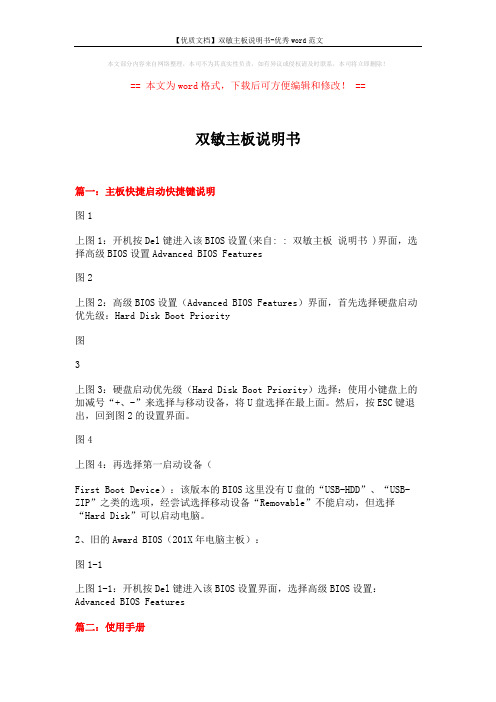
本文部分内容来自网络整理,本司不为其真实性负责,如有异议或侵权请及时联系,本司将立即删除!== 本文为word格式,下载后可方便编辑和修改! ==双敏主板说明书篇一:主板快捷启动快捷键说明图1上图1:开机按Del键进入该BIOS设置(来自: : 双敏主板说明书 )界面,选择高级BIOS设置Advanced BIOS Features图2上图2:高级BIOS设置(Advanced BIOS Features)界面,首先选择硬盘启动优先级:Hard Disk Boot Priority图3上图3:硬盘启动优先级(Hard Disk Boot Priority)选择:使用小键盘上的加减号“+、-”来选择与移动设备,将U盘选择在最上面。
然后,按ESC键退出,回到图2的设置界面。
图4上图4:再选择第一启动设备(First Boot Device):该版本的BIOS这里没有U盘的“USB-HDD”、“USB-ZIP”之类的选项,经尝试选择移动设备“Removable”不能启动,但选择“Hard Disk”可以启动电脑。
2、旧的Award BIOS(201X年电脑主板):图1-1上图1-1:开机按Del键进入该BIOS设置界面,选择高级BIOS设置:Advanced BIOS Features篇二:使用手册目录第一章系统简介 .................................................................. . (3)一、软件简介 .................................................................. ......................................................... 3 二、系统特性 .................................................................. ......................................................... 3 三、环境需求 .................................................................. ......................................................... 3 第二章产品安装 .................................................................. . (5)一、驱动安装 .................................................................. (5)1、自动安装 .................................................................. ................................................... 5 2、手动安装 .................................................................. ................................................... 6 3、驱动程序卸载 .................................................................. ......................................... 10 二、服务器程序安装 .................................................................. ........................................... 10 第三章服务器端说明 .................................................................. .. (12)一、主界面介绍 .................................................................. (12)1、右控制面板 .................................................................. ............................................. 14 2、下控制面板 .................................................................. ............................................. 17 二、系统设置 .................................................................. . (18)1、系统选项 .................................................................. ................................................. 19 2、视频参数 .................................................................. ................................................. 23 3、视频设置 .................................................................. ................................................. 25 4、动态检测 .................................................................. ................................................. 25 5、I/O设置 .................................................................. .................................................. 26 6、云台控制 .................................................................. ................................................. 28 8、历史记录 .................................................................. ................................................. 30 9、拔号报警 .................................................................. ................................................. 30 10、网络 .................................................................. ....................................................... 30 三、备份 .................................................................. . (31)四、回放 .................................................................. ....................................................... 33 五、浏览图像 .................................................................. ....................................................... 34 六、升级 .................................................................. ............................................................... 35 第四章网络访问 .................................................................. . (36)一、Netplay访问 .................................................................. . (36)1、Netplay安装 .................................................................. ........................................... 36 2、打开Netplay ............................................................. ................................................ 36 3、Netplay的设。
486DateSYSTEM MEMORY. . . . . . . . 11 MEMORY CONFIGURATION . . . . . . 11 CACHE CONFIGURING SIZE .: : : : : : 16 DAYLIGHT SAVING17 LOAD SETUP DEFAULT’ : : : : : : FEATURESH A R D D I S K S P E C I F I C A T I O N S. . . 25CONNER . . . . . . . . . . . . . . . . . . . . . . . . . 25QUANTUM . . . . . . . . . . . . . . . . . . . . . . . . 26: : : : : : : :OVERVIEW INTRODUCTIONThe80486180386 PC/ATof direct mapped write-back cache memory.Supportsincludes built- in 8042 keyboard controller.SYSTEM BLOCK DIAGRAMVESA BUSCache, ISAISA BUSDATABUSDRAM3MOTHERBOARD SETTINGS CONNECTORConnector Function Pin outs Signal nameCN2Power1Power goodconnector24GND912Turbo LED 1v c c2LEDHardware1GNDreset2Reset signalJ12Speaker1Speaker signalconnector2NC3GND4JUMPER DESCRIPTIONJumper Function OpenClose J7Password2-3(For o n l y)TABLE /VOTE: # REFERANCE PAGE CPUJC36CPU CLOCK SELECTION5-63-4l-2CLK2010080 MHZ010166.6 MHZ10040 MHZ1101CONNECTORThe motherboard provides two high-performance VESA bus connectors,on the board component side.“Side B” of the connector are for theConnector 121314151617181920212223242526272829303132333435363738394041424344454849505152535455565758GND DAT17v c c DAT23DAT25GND DAT27DAT29DAT3 1ADR08GNDADR06GNDSidepinsDATOO DAT02DAT04DAT06DAT08GNDDAT30v c c ADR31GND ADR29ADR27ADR25ADR23GND ADR171ADR09ADR07ADR05GND ADR03ARD02NCRESConnector SL160102030405060708091011121314151617DATO 1DAT07DAT13DAT2ADR18ADR16ADS#v c c ID2ID3ID4Side E01020304050607080910GNDADR17GND ADR03ADR02NC RESGNDThe CPU Speed jumper settings follow the maximum clock speed of the CPU in use. Adjust the setting according to your CPU clock speed.CPU SpeedMHzMEMORY MEMORY CQNFIGURATION486System Bank0Bank165MB256K x 4256K x 468MBCACHE CONFIGURING SIZEThe cache size of 486-KVD motherboard is jumper-selectable.are assigned as Bank 1.64KBANK0TAG RAM1-2 shorted2-3 shorted2-3 shorted2-3 shorted2-3 shorted1-2 shortedM6128Kbytes Direct Mapped Cache256Kbytes Direct Mapped CacheM4AWARD BIOS SETUP SYSTEM SETUPA SETUP program, built into the system BIOS, is stored in the CMOS RAM that allows the configuration settings to be changed. This program is executed when:key.Press orAWARD SOFTWARE, INCSTANDARD CMOS SETUP PASSWORD SETTINGBIOS FEATURES SETUP IDE HDD AUTO DETECTIONExit 3 :SelectItemor “ENTER” to run the select program.STANDARD CMOS SETUPThe Standard CMOS Setup has 10 items for setting.Each item may have one or more option settings.Use the arrow keys to highlight the item and then use the5.25 in 3.5 inAll ErrorsHEADS PRECOMPMemory8192KEsc : Quit: Select Item:ModifL F3function key toDAYLIGHT SAVINGWhen enabled, this field allows user to Set the clock one hour in advance.When disabled, it subtracts one hour when standard time begins. After the changes are made, pressBIOS FEATURES SETUPROM ISA BIOS (VIAOOOOO)BIOS FEATURES SETUPAWARD SOFTWARE, INC.CPU Internal Cache External CacheQuick Power On Self Test Boot SequenceBoot Up Floppy Seek Boot Up Numlock Status Boot UP System Speed IDE HDD Block Mode Gate A20 Option Typematic Rate SettingTypematic RateE n a b l e dOnD i s a b l e d 6 SetupSystem BIOS ShadowE n a b l edShadow D i s a b l ed Shadow D i s a b le dESCItemHelpOld Values (Shift) F2 Load BIOS Defaults F7FEATURES SETUP84 K Video BIOS Cacheable System BIOS Cacheabl e DRAM Timing Comtrol Cache Timing ControlD i s a b l e dD i s a b l e dE n a b l e dTurboESCItemHelpOld Values (Shift) F2 Load BIOS Defaults F7FEATURE SETUP programsshown above work the same way as moving around the standard CMOSSETUP program. Users are not encouraged to run the BIOS andPASSWORD SETTINGWhen you select this function, you can create a password. Type YOUR password up to eight characters and pressYou may also pressEXITING SETUPROM ISA BIOS (VIAOOOOO)CMOS SRTUP UTILITYAWARD SOFTWARE, INC.STANDARD CMOS SETUP PASSWORD SETUPBIOS FEATURES SETUP IDE HDD AUTO DETECTIONETUPSAVINGESCExit Setup S el ect Itemto returnto the main menu.Move cursor to “SAVE & EXIT SETUP” or pressto retain the SETUP settings.AM1 BIOS SETUP SYSTEM SETUPA SETUP program has been built into the system BIOS so that configurations stored in the CMOS RAM can be changed. This program is exectud when:if you want to run SETUP.”Press “DEL” to run setup or do nothing to bypass.If the “DEL” key pressed, the following screen is displayed:AM1 BIOS SETUP PROGRAMRights ReservedADVANCED CMOS SETUPAUTO CONFIGURATION WITH BIOS DEFAULTSAUTO CONFIGURATION WITH POWER-ON DEFAULTSCHANGE PASSWORDAUTO DETECT HARD DISKHARD DISK UTILITYWRITE TO CMOS AND EXITDO NOT WRITE TO CMOS AND EXITStandard CMOS Setup for Changing Time, Date, Hard Disk Type, etc.ESC ExitUse7 8 9 10 1112Installed20 21 22 23 24 252627 28 29 30 31 1 2Esc Selectis completely menu driven.Use the arrow keys to select an entry; keys to change an entry; and “Esc” key to exit.Help messages are displayed in a window on the screen whenkeys are pressed.The standard CMOS SETUP screen is shown above.System BIOS automatically detects memory size, thus no changes are necessary.After the changes are made, press “Esc” to exit.Typematic Rate ProgrammingD i s a b l e dMemory Test Tick SoundMessage DisplayE n a b l e d System Boot Up Num Lock E n a b l e d Weitek Processor Enabled System Boot Up Sequence High External Cache Memory Enabled Fast Gate A20 OptionSetupVideo ROM Shadow COOO, 32K32K 64KVirus Protection E n a b l e d Video Cacheable OptionD i s a b l e d Extended ALED i s a b l e dAUTOBus Clock Rate Select Cache Read Cycle Select Cache Write Cycle SelectESC: ExitBIOS Setup Defaultsto return to the main meun, move cursor to “Write to CMOS and Exit”, and pressagain and pressExit ExitMODEL CYLINDER SECTOR 85MB5268CP-30084E 526839CP-30104120MB7268396831638CP-30254 8951055360MBCP-3544 10241663 MAXTORMODEL CAPACITY CYLINDER HEAD SECTOR170MB9841034MODEL CAPACITY CYLINDER HEAD SECTOR7551620AT240MB72385MB977IO17170MB10111522MODEL CAPACITY CYLINDER85MB1024IO17ST31 20A102MB10241210011517872835AC2200200M9891235。
硬件安装指导手册1. 准备工作在进行硬件安装之前,确保您已经完成以下准备工作:- 阅读并理解硬件安装手册中的说明。
- 将所有所需的硬件组件、配件和工具准备好。
- 关闭计算机电源并断开所有电源连接。
2. 硬件清单在开始硬件安装之前,确保您已经准备了以下硬件组件和配件:- 主板- 中央处理器(CPU)- 内存条(RAM)- 显卡- 硬盘- 电源供应器- 散热器- 数据线和电源线- 相应的螺丝和螺丝刀- 其他配件(如风扇、散热胶等)3. 安装主板按照以下步骤安装主板:- 将主板放置在计算机机箱内的主板托架上。
- 使用螺丝固定主板,确保主板稳固地安装在机箱内。
- 连接主板与计算机机箱前面板上的按钮和指示灯。
4. 安装中央处理器(CPU)- 根据主板和CPU的类型,打开CPU插槽的保护盖。
- 将CPU插入插槽中,确保CPU引脚与插槽对应。
- 轻轻按下CPU,使其安全地插入插槽。
- 关闭CPU插槽的保护盖。
5. 安装内存条(RAM)- 打开主板上的内存插槽保护盖。
- 将内存条对准内存插槽口,轻轻按下,直到锁定。
- 关闭内存插槽保护盖。
6. 安装显卡- 将显卡插入主板上的PCI-E插槽中,确保插卡口完全插入,并与机箱后面板上的外接口对齐。
- 使用螺丝固定显卡。
7. 安装硬盘- 将硬盘插入计算机机箱内的硬盘托架中。
- 使用螺丝固定硬盘。
8. 连接电源供应器和数据线- 将电源供应器插头连接到主板的电源插槽上。
- 连接硬盘和其他外设的数据线。
9. 安装散热器- 将散热器安装在中央处理器上,使用散热胶固定。
- 连接散热器的风扇插头到主板上的相应插槽。
10. 检查和启动- 检查所有连接是否牢固,确保没有松动的插头或线缆。
- 连接显示器、键盘和鼠标到计算机。
- 连接电源并启动计算机。
11. 故障排除如果计算机无法启动或出现其他问题,请参考以下故障排除步骤:- 检查电源线是否正确连接到电源插座。
- 确保所有硬件组件的连接牢固。
梅捷AMD系列主板说明书适用于:AMD系列芯片组说明书版本V1.7更新日期2014年5月30日梅捷简体中文网站/梅捷中国大陆技术支持E-mail:梅捷官方微博/soyo1999梅捷中国大陆服务电话************版权声明:说明书版权归梅捷科技所有。
梅捷科技有权在不知会用户的前提下增益、删除内容。
本说明书为纯技术文档,无任何暗示及映射第三方内容。
且不承担因印刷及排版错误而导致的任何歧义。
本说明书中所涉及之任何第三方之注册商标,所有权归其制造商或品牌供应商所有。
Copyright©1999——2014版权所有、未经授权,禁止以任何方式复制传播。
关于本手册:本说明书适合初学者,包含相关产品特性介绍及软体安装介绍,以及一些名词的解释。
本说明书可以作为技术性参考资料,用户使用时请以实物为准。
非正常保修范围:1、产品因不当使用与安装,自行拆解或更换零件,或是任意变更规格所造成的故障与损坏,不在保修范围内。
2、产品一经变更或修改,以及任何因间接、特殊或意外情况所造成的损害,不在保修范围内。
避免在下列环境中使用本产品:高温、低气压、低温、潮湿、多尘、磁场强大及长期暴露于阳光之下。
本公司建议您在海拔3000米以下,0°至35°C,湿度为5%至95%的环境中使用。
FCC条款:本装置完全遵循FCC条款第15部分的规定。
遵照下列两项条件来作业:1、本装置不会造成人身伤害;2、本装置必须能接受任何已回复的冲突干扰,包括可能会造成不当操作的冲突。
注意:依照FCC条款第15部分规定,本装置已经通过测试并且符合Class B数位装置的限制。
这项限制是为了安装过程中可能造成的伤害性冲突的合理防范措施。
本装置产生、使用、并且可以发射无线电的频率能量,但如果没有依照制造商的指示安装和使用,可能会与通讯工具造成伤害性冲突。
然而,并不保证在特定的安装下不会产生任何冲突。
如果关闭和重开本装置后,仍确定本装置真的造成收音机或电视机的冲突,请使用者利用下列一项或多项知识来更正所造成的冲突:●重新安装接收天线;●增加装置与受讯器间的分隔;●将电脑插入不同的插座以便于两个装置使用不同的回路。
SV1-D4212 Motherboard User Guide Version 1.1
Intel Pineview + NM10 Two-Chip Solution Up to 2 GB DDR3 1333/1066/800 SDRAM, 1 SO-DIMM Seavo Second Generation Multi-Function Card supported 1 Onboard PCI-E 100Mbps Ethernet 2 COM, 8 USB, 2 SATA, 1 Mini PCI-E, HDA, Mini-ITX - 1 - 深圳市信步科技有限公司 地址:深圳市福田区车公庙泰然工贸园210栋西座5H T 86-755-88251900 F 86-755-88251910 www.seavo.com
Specification CPU Intel Atom D425 1.8 GHz BGA CPU With IMC , GPU and IIO integrated Chipset Intel NM10 , with max TDP 2.1 W
Graphic Interface Integrate Intel GMA 3150 graphic core Support DX9.0c
Memory Support DDR3 1333/1066/800 MHz 1 * SO-DIMM slot,Maximum voltage of 2 GB
Storage Intel Serial ATA2 (3 Gbps) controller 2 * Serial ATA ports
Ethernet Realtek 8103EL PCI-E Fast Ethernet Controller
Support 10/100 Mbps with RJ45
Audio Realtek ALC662 5.1 Channel HD Audio Codec Support Line-in/Line-out Ports(onboard header)
Seavo M-Card Seavo Second Generation Multi-function Sub-Card Connector (support SV-M2-GH : HDMI + VGA SV-M2-4S : 4 * SATA SV-M2-GH4S : HDMI + VGA + 4 * SATA SV-M2-LG : LVDS + VGA SV-M2-P : DC12V Input SV-M2-PLG : DC12V Input + LVDS + VGA ) COM 2 * COM ports
Other Ports 8 * USB2.0 (4 Onboard header and 4 on panel) 2 * VGA 1 * PS/2 keyboard and mouse ports (internal pin connector) 1 * ATX 20Pin power socket 1 * CPU fan socket 1 * PCI slot 1 * LPT Factor Mini ITX - 2 - 深圳市信步科技有限公司 地址:深圳市福田区车公庙泰然工贸园210栋西座5H T 86-755-88251900 F 86-755-88251910 www.seavo.com
Jumper and Header Locations - 3 -
深圳市信步科技有限公司 地址:深圳市福田区车公庙泰然工贸园210栋西座5H T 86-755-88251900 F 86-755-88251910 www.seavo.com - 4 -
深圳市信步科技有限公司 地址:深圳市福田区车公庙泰然工贸园210栋西座5H T 86-755-88251900 F 86-755-88251910 www.seavo.com
Definition of Jumpers and Headers [1] Front Panel Header(5*2 Pin 2.54 mm) Pin Definition Pin Definition 1 HD + 2 MSG/PD+ 3 HD - 4 MSG/PD- 5 GND 6 PW+ 7 RESET 8 PW- F_PANEL1 9 N/C 10 N/A
[2] CMOS Control Jumper (3*1Pin 2.54 mm) Setting Instruction 1-2 Normal CLR_CMOS
2-3 Clear CMOS
[3] USB Header(5*2 Pin 2.54 mm) Pin Definition Pin Definition 1 + 5 V 2 + 5 V 3 USB0- 4 USB1- 5 USB0+ 6 USB1+ 7 GND 8 GND F_USB1,2 9 N/A 10 N/C
[4] Audio Header(5*2 Pin 2.54 mm) Pin Definition Pin Definition 1 FP_MIC_R 2 GND 3 FP_MIC_L 4 +3.3 V 5 FP_OUT_R 6 GND 7 Jack Detect 8 N/A JP9 9 FP_OUT_L 10 GND - 5 - 深圳市信步科技有限公司 地址:深圳市福田区车公庙泰然工贸园210栋西座5H T 86-755-88251900 F 86-755-88251910 www.seavo.com
[5] LCD Backlight Control Header(5*1 Pin 2.00 mm) Pin Definition Pin Definition 1 + 12V 2 GND 3 BKL_EN 4 BKL_PANEL(adjust rightness ) JP4 5 + 5V
[6] LVDS Interface Voltage Selection (2.0mm) Pin Definition Pin Definition 1 + 3.3V 2 VDD_PANEL JP1/JP2
3 + 5V
[7] VGA Header(2*8 Pin 2.00 mm) Pin Definition Pin Definition 1 RED 2 + 5V 3 GREEN 4 GND 5 BLUE 6 + 5V 7 N/C 8 S_DATA 9 GND 10 HSYNC 11 GND 12 VSYNC 13 GND 14 S_CLOCK VGA2
15 GND 16 N/A
[8] GPIO Header(3*2 Pin 2.00 mm) Pin Definition Pin Definition 1 + 3.3 V 2 GPIO9 3 GPIO7 4 GPIO10 JP15 5 GPIO8 6 GND
Pin Definition Pin Definition 1 GPIO36或N/A 2 GPIO51 3 GPIO37 4 GPIO52 JP12 5 + 5 V 6 GND - 6 - 深圳市信步科技有限公司 地址:深圳市福田区车公庙泰然工贸园210栋西座5H T 86-755-88251900 F 86-755-88251910 www.seavo.com
[9] Serial Port 2 Connector(5*2 Pin 2.0 mm) Pin Definition Pin Definition
1 JP11* 2 RXD 3 TXD 4 DTR 5 GND 6 DSR 7 RTS 8 CTS COM 2
9 JP11* 10 N/A * Please refer to Table[11]。
[10] Serial Port Control Jumper (2.0mm) Jumper Settings Serial Port Function 1-3 Pin 1 Output:+5V 2-4 Pin 9 Output:+12V 3-5 Pin 1 Output:DCD JP11
4-6 COM2 Pin 9 Output:RI 1-3, 5-7 Pin 2 Output:RXD(RS232电平) 2-4, 6-8 Pin 3 Output:TXD(RS232电平) 3-5 Pin 2 Output:RXD(TTL电平) JP7 4-6 COM3 Pin 3 Output:TXD(TTL电平)
[11] Seavo M-Card Connector(10*2 Pin 2.54 mm)
J1&J2 The second generation of Seavo Multi-function Sub-Card support plenty of factions ,such as HDMI, DVI, VGA, LVDS, TV(S/ AV), Mini PCI-E, Wi-Fi, SATA etc.
[12] PS/2 Keyboard and Mouse Control Header(5*2 Pin 2.54 mm) Pin Definition Pin Definition 1 + 5 V 2 GND 3 KB_CK2 4 KB_DT2 5 KB_CK1 6 KB_DT1 7 MS_CK2 8 MS_DT2 PS2_CON
9 MS_CK1 10 MS_DT1