基于低电压高线性度的变频混频器设计
- 格式:pdf
- 大小:207.41 KB
- 文档页数:4
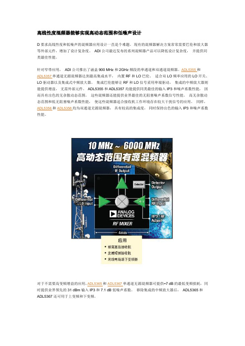
高线性度混频器能够实现高动态范围和低噪声设计D要求高线性度和低噪声的混频器应用设计一直是个难题。
现有的混频器解决方案常常需要巴伦和放大器等外部元件,增加了设计复杂度。
ADI公司最近发布的系列混频器产品可以降低设计复杂度,并提供同类最佳性能。
针对窄带应用,ADI公司推出了涵盖900 MHz和2GHz频段的单通道和双通道混频器。
ADL5355和ADL5357单通道无源混频器达到最高集成水平,内置RF和LO巴伦、适合双LO频率应用的LO开关、LO驱动器以及集成式中频放大器。
集成巴伦能够让RF和LO信号采用单端驱动,集成的中频放大器则能提供增益,无需外部元件。
ADL5355和ADL5357均能提供同类最佳的输入IP3和噪声系数性能,因而具有出色的无杂散动态范围。
这些混频器还能提供业界最佳的无阻塞噪声系数信号性能。
高无杂散动态范围和低无阻塞噪声系数性能,使这些混频器适合接收机工作环境存在较大干扰信号的应用。
同样,ADL5356和ADL5358均为双通道无源混频器,具有较高的集成度,同时保持出色的输入IP3和噪声系数性能。
对于不需要高变频增益的应用,ADL5365和ADL5367单通道无源混频器可提供–7 dB的最低变频损耗,同时提供业界领先的31 dBm输入IP3和7.1 dB低噪声系数。
移除集成的中频放大器后,ADL5365和ADL5367还可用于上变频和下变频。
这些无源单、双通道混频器设计采用3.3 V ~ 5 V电源供电,并采用先进的SiGe双极性工艺制造,提供2000 V人体模型ESD保护,因此与敏感的GaAs混频器相比能简化处理程序。
对于宽带混频器应用,ADI公司最近推出了ADL5801和ADL5802宽带有源混频器,其工作频率范围为10 MHz ~ 6000 MHz,在现有混频器中最宽。
这两款混频器均提供1.5 dB的变频增益,无需附加中频放大器。
这些有源混频器提供同类最佳的无阻塞噪声系数信号性能和无杂散动态范围。

基于电流模结构的超宽带无源混频器设计
李潇然;王乾;雷蕾;刘自成;韩放;齐全文;王兴华
【期刊名称】《北京理工大学学报》
【年(卷),期】2024(44)6
【摘要】采用SMIC 55 nm CMOS工艺,提出基于电流模结构的2~8 GHz超宽带高线性度直接下变频无源混频器结构.本设计主要结构为低噪声跨导放大器(low noise transconductance amplifier,LNTA)驱动I/Q两路电流模无源混频器,负载为低输入阻抗的跨阻放大器(trans-impedance amplifier,TIA),即LNTA-Passive Mixer-TIA结构.LNTA采用电容交叉耦合以及双端正反馈结构,解决阻抗匹配以及噪声等关键参数的折中问题.整个接收机链路获得较好的线性度及噪声性能,对于电源电压以及衬底噪声的鲁棒性也有所提升.后仿结果表明,在电源电压1.2 V情况下,射频输入信号频率为2~8 GHz,1 dB压缩点为−5.5 dBm,带内输入三阶交调点为−1 dBm,整体噪声系数为4 dB,核心版图面积为0.12 mm^(2).
【总页数】6页(P655-660)
【作者】李潇然;王乾;雷蕾;刘自成;韩放;齐全文;王兴华
【作者单位】北京理工大学集成电路与电子学院;北京理工大学前沿技术研究院;北京理工大学重庆微电子研究院;北京理工大学长三角研究院(嘉兴)
【正文语种】中文
【中图分类】TN432
【相关文献】
1.基于无源混频器的多频段TD-SCDMA射频接收器前端设计
2.基于电流模电路的通用宽带电流放大器的设计与仿真
3.基于微带无源电路的宽带毫米波分谐波混频器
4.一款应用于超高频射频识别标签的低功耗电流模无源混频器
因版权原因,仅展示原文概要,查看原文内容请购买。
第37卷第2期2017年6月雷达与对抗RADAR&ECMVol. 37 No. 2Jun.2017一种S波段高线性度下变频模块的设计闫超,赵家敏,姚武生(中国电子科技集团公司第三十八研究所,合肥230088)摘要:描述了一种应用于S波段接收通道的高线性度下变频模块设计,针对模块的增益、线 性度、杂谐波抑制等关键技术指标进行了详细的理论和仿真分析,并硬件实现了该模块。
该模 块主要采用SM D器件,包括有源混频器、高0IP3放大器和L C滤波器等。
测试结果显示,模块增益为21 d B,杂谐波抑制度大于65 dB c,对特定频点的抑制度大于40 dBc,IIP3大于24 dBm,表明该模块满足指标要求,能够充分适应高性能接收通道的应用要求。
关键词:下变频模块;增益;线性度;杂谐波抑制中图分类号:TN850 文献标志码:A 文章编号:1009 -0401(2017)02-0055 -05 Design of an S-band high-linearity down conversion moduleYAN Chao, ZHAO Jia-min, YAO Wu-sheng(No. 38 Research Institute of CETC, Hefei 230088)Abstract :A high-linearity down conversion module is designed for the S-band receiving channel. The key technical specifications such as the gain, linearity as well as spurious and harmonic wave suppression are simulated and analyzed theoretically in detail with the hardware implemented. The module mainly adopts the SMD devices, including the active mixer, the high-0IP3 amplifier and the LC filter. The test results show that the gain of the module is 21 dB, the spurious and harmonic wave suppression is greater than 65dBc, the suppression of the specific frequency is more than 40dBc, and the IIP3 is greater than 24dBm, indicating that the module meets the requirements, and can fully meet the application requirements of the high-performance receiving channel. Keywords :down conversion module;gain ;linearity ;spurious and harmonic wave suppression〇引言现代通信、雷达接收机大多采用超外差接收体制,下变频器是超外差接收机的关键组成部分。
SSOP20:plastic shrink small outline package; 20 leads; body width 4.4 mm SOT266-1Philips Semiconductors and Philips Electronics North America Corporation reserve the right to make changes, without notice, in the products,including circuits, standard cells, and/or software, described or contained herein in order to improve design and/or performance. Philips Semiconductors assumes no responsibility or liability for the use of any of these products, conveys no license or title under any patent, copyright,or mask work right to these products, and makes no representations or warranties that these products are free from patent, copyright, or mask work right infringement, unless otherwise specified. Applications that are described herein for any of these products are for illustrative purposes only. Philips Semiconductors makes no representation or warranty that such applications will be suitable for the specified use without further testing or modification.LIFE SUPPORT APPLICATIONSPhilips Semiconductors and Philips Electronics North America Corporation Products are not designed for use in life support appliances, devices,or systems where malfunction of a Philips Semiconductors and Philips Electronics North America Corporation Product can reasonably be expected to result in a personal injury. Philips Semiconductors and Philips Electronics North America Corporation customers using or selling Philips Semiconductors and Philips Electronics North America Corporation Products for use in such applications do so at their own risk and agree to fully indemnify Philips Semiconductors and Philips Electronics North America Corporation for any damages resulting from such improper use or sale.This data sheet contains preliminary data, and supplementary data will be published at a later date. Philips Semiconductors reserves the right to make changes at any time without notice in order to improve design and supply the best possible product.Philips Semiconductors 811 East Arques Avenue P .O. Box 3409Sunnyvale, California 94088–3409Telephone 800-234-7381DEFINITIONSData Sheet IdentificationProduct StatusDefinitionObjective SpecificationPreliminary Specification Product Specification Formative or in DesignPreproduction ProductFull ProductionThis data sheet contains the design target or goal specifications for product development. Specifications may change in any manner without notice.This data sheet contains Final Specifications. Philips Semiconductors reserves the right to make changes at any time without notice, in order to improve design and supply the best possible product.© Copyright Philips Electronics North America Corporation 1997All rights reserved. Printed in U.S.A.。
射频与微波一种低噪声高线性度C MO S上变频混频器Ξ金黎明 倪熔华 唐长文ΞΞ 闵 昊(复旦大学专用集成电路与系统国家重点实验室,上海,201203)2007210215收稿,2008201202收改稿摘要:设计实现了一种采用开关跨导型结构的低噪声高线性度上变频混频器,详细分析了电路的噪声特性和线性度等性能参数,本振频率为900M H z。
芯片采用0118Λm M ixed signal C M O S工艺实现。
测试结果表明,混频器的转换增益约为8dB,单边带噪声系数约为11dB,输入参考三阶交调点(IIP3)约为1015dBm。
芯片工作在118V 电源电压下,消耗的电流为10mA,芯片总面积为0163mm×0178mm。
关键词:混频器;开关跨导;噪声系数;三阶交调点中图分类号:TN4 文献标识码:A 文章编号:100023819(2008)032363205A L ow No ise H igh L i near ity C MOS Upconversion M ixerJ I N L i m ing N I Ronghua TAN G Zhangw en M I N H ao(S tate K ey L aboratory of A S IC and S y ste m,F ud an U niversity,S hang hai,201203,CH N)Abstract:In th is pap er,a low no ise h igh linearity m ixer is p resen ted,exp lo iting a s w itched tran sconducto r topo logy.Its no ise figu re(N F)and linearity are analyzed particu larly.T he LO frequency is900M H z.T he m ixer ch i p is i m p lem en ted in0118Λm m ixed signal C M O S p rocess. T he m easu rem en t resu lt show s that the conversi on gain of the m ixer is abou t8dB,the SSB N F is abou t11dB,and the inpu t2referred th ird2o rder in tercep t po in t(IIP3)is abou t1015dBm.T he ch i p con sum es10mA at118V pow er supp ly and the size of the w ho le ch i p is0163mm×0178mm.Key words:m ixer;switched tran sconductor;no ise f igure;th ird-order i n tercept po i n tEEACC:12501 引 言混频器主要分为有源和无源两种类型[1]。
高线性度有源混频器的设计李桂琴;宋树祥;岑明灿;刘国伦;谢丽娜【摘要】针对吉尔伯特混频器电路转换增益和线性度低的问题,设计了一个高转换增益﹑高线性度下变频有源混频器,其电路跨导级采用电流镜结构和第三阶跨导系数消除结构,通过设置晶体管工作在不同的区域,使得晶体管的第三阶跨导系数相互消除,以提高电路的转换增益和线性度.电路采用TSMC 0.18μm RF CMOS工艺.Cadence Spectre-RF软件仿真结果表明,在工作电压为1.2 V﹑射频频率为5.2 GHz﹑本振频率为5 GHz﹑中频频率为200 MHz时,所设计的混频器电路的转换增益为21.9 dB,噪声系数为16.5 dB,线性度(输入三阶交调点IIP3)为21.68 dBm,功耗为2.3 mW,转换增益由典型指标10 dB提升至21.9 dB,线性度由典型指标5 dBm提升至21.68 dBm.可见,所设计的混频器电路的转换增益和线性度得到有效改善.【期刊名称】《广西大学学报(自然科学版)》【年(卷),期】2018(043)006【总页数】7页(P2184-2190)【关键词】混频器;吉尔伯特;转换增益;Cadence;线性度【作者】李桂琴;宋树祥;岑明灿;刘国伦;谢丽娜【作者单位】广西师范大学电子工程学院,广西桂林 541004;广西师范大学电子工程学院,广西桂林 541004;广西师范大学电子工程学院,广西桂林 541004;广西师范大学电子工程学院,广西桂林 541004;广西师范大学电子工程学院,广西桂林541004【正文语种】中文【中图分类】TN7730 引言随着无线通信技术在手机、蓝牙、物联网等领域应用越来越广泛,对无线通信设备的要求也越来越高,因此,射频接收机成为当前的研究热点。
混频器作为射频接收机中的重要模块,对其性能要求很高,提高混频器的性能指标即可以提高射频接收机前端的性能指标[1-3]。
根据不同的国家应用,手机支持的 IEEE 802.11a 标准工作频段在4.9~5.85 GHz,国际 802.11a 标准的工作频率是5.2 GHz,因此,5.2 GHz 频率在混频器中的应用得到快速发展。
凌特公司推出高线性度有源RF混频器
佚名
【期刊名称】《电子与电脑》
【年(卷),期】2005(000)005
【摘要】凌特公司(Linear Technology)新的高线性度有源下变频RF混频器极大地降低3G蜂窝基站的成本并简化其设计。
LT5527RF混频器具有延至3.7GHz 的工作频率范围。
在1.9GHz时,LT5527具有23.5dBrm的ⅡP3(输入3阶截取)线性度、2.3dB转换增益和12.5dB噪声指标,从而满足了3G蜂窝基站和其它高性能无线基础设施接收器的动态范围要求。
【总页数】1页(P24)
【正文语种】中文
【中图分类】TP213
【相关文献】
1.凌特公司推出射频有源发送混频器 [J], 敖琼
2.ADI推出高线性度RF混频器ADL5350 [J], 无
3.凌特推出RF有源混频器LT5525和LT5526 [J], 无
4.凌特推出变频RF有源混频器 [J], 无
5.凌特公司新推出两款高线性度有源上变频混频器 [J],
因版权原因,仅展示原文概要,查看原文内容请购买。