16位微处理器
- 格式:ppt
- 大小:1.45 MB
- 文档页数:99
8086结构组成8086是一款16位微处理器,它的结构组成非常复杂。
本文将从以下几个方面来详细介绍8086的结构组成。
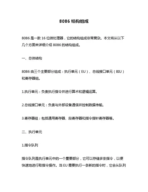
一、总体结构8086由三个主要部分组成:执行单元(EU)、总线接口单元(BIU)和寄存器组。
1.执行单元:负责执行指令并进行算术和逻辑运算。
2.总线接口单元:负责与外部设备通信并控制数据传输。
3.寄存器组:包括通用寄存器、段寄存器和指令指针寄存器等。
二、执行单元1.指令队列指令队列是执行单元中的一个重要部分,它可以存储多条指令,以便快速地进行取指令操作。
当EU需要执行一条新的指令时,它会从队列中取出下一条指令并开始执行。
2.算术逻辑单元算术逻辑单元(ALU)是执行单元中的核心部分,它可以进行各种算术和逻辑运算,如加、减、乘、除、与、或等操作。
ALU还可以处理条件跳转和无条件跳转等控制操作。
3.状态标志寄存器状态标志寄存器(FLAGS)用于记录ALU运算的结果,以便EU进行下一步操作。
FLAGS寄存器包括零标志位、进位标志位、溢出标志位等。
三、总线接口单元1.地址加法器地址加法器(AFA)是BIU的核心部分,它可以将内部地址转换为外部地址,并控制数据传输。
2.指令缓存器指令缓存器(IC)用于存储从内存中读取的指令。
当EU需要执行一条新的指令时,BIU会从IC中取出相应的指令并传输给EU。
3.数据缓存器数据缓存器(DC)用于暂时存储从内存中读取或写入的数据。
当EU 需要访问内存时,BIU会将相应的数据传输到DC中,EU再从DC中读取或写入数据。
四、寄存器组1.通用寄存器8086有8个16位通用寄存器,分别命名为AX、BX、CX、DX、SI、DI、BP和SP。
这些寄存器可以用于保存临时数据和计算结果等。
2.段寄存器8086有4个16位段寄存器,分别命名为CS、DS、ES和SS。
这些寄存器用于保存程序和数据在内存中的位置信息。
3.指令指针寄存器指令指针寄存器(IP)用于保存下一条指令在内存中的地址。
most demanding needsM icrocontrollerPrecision AnalogSecurityLow-Power OperationIndustry's best securitytechnology to protect money, software IP, or secret dataWorld-class low power and high performance to make today’s battery-powered equipment run faster and longerPrecision analog to support complex, mixed-signal embedded applicationsMaxim is a registered trademark of Maxim Integrated Products, Inc. © 2009 Maxim Integrated Products, Inc. All rights reserved.Give your customer months of extra time 16-bit MAXQ® µCs greatly extend battery life in portable equipment The MAXQ610 is designed for low-cost, high-performance, battery-powered applications. This 16-bit, RISC-basedconsumption. Its anticloning features and secure MMU enable you to protect your IPMicrocontroller• 16-bit MAXQ RISC core• 64KB flash memory, 2KB SRAM• Ultra-low supply current• Active mode: 3.75mA at 12MHz• Stop mode: 200nA (typ), 2.0µA (max)• Wide, 1.7V to 3.6V operating voltage range • IP protection• Secure MMU supports multiple privilegemaster/slave • Two 16-bit timers/counters• 8kHz nanoring functions as programmable wakeup timerMaxim’s line of low-power µCs are designed to specifically address the most pressing demands on today’s battery-powered electronics. These µCs extend battery life, enable advanced feature sets through higher performance and integration, and allow small form factors with reduced footprint solutions.KEYPAD MATRIXGPIOsSECURE, 16-BIT MAXQ COREMAXQ610Supports capacitive touch or pushbutton matrixDirectly drive IR transmission up to 25mA Operates down to 1.7V—ideal for 2AA/AAA batteries!Learning or fixed-function remoteApplication focus: Universal remote controlsMaxim now offers the widest range of devices with integrated infrared drivers and timers for IR communications, due to its acquisition of the Classic IR and Crimzon ® lines from Zilog. Combined with the unmatched ability to extend battery life and integrate multiple features, Maxim’s µCs are the ideal choice for remote-control designs.Need a PCI 2.0 silicon provider?Look no furtherThe universal secure integrated platform professional IC (USIP™ PRO) is the industry’s highest performance, most secure 32-bit MIPS® microprocessor. It supports Linux® operating systems and enables next-generation EMV® and PCI PED-compliant applications.With the acquisition of Innova Card and the secure transaction Zatara® product line from Zilog, the secure µC product line from Maxim now offers the broadest range of products for the high-security, financial-terminal market. Combining Maxim’s high-security silicon technology, Innova Card’s application knowledge and support, and Zatara’s impressive integration, Maxim now has the best knowledge, technology, and products to support the most demanding security applications.Secure microcontrollersIndustry’s fastest, most secure ARM®-based SoC µC meets PCI 2.0 requirementsIntegrates security and application-management functions needed for the next generation of trusted devicesEXTERNAL BUS CONTROLLERLowest pin count, secure µC for financial-terminal applicationsSmallest footprint available for applications that require a high level of physical and logical security32-bit µC integrates security supervisor and cryptographic functionsIdeal for any application that requires PCI, FIPS 140-2, Common Criteria, or other security certificationsElectricity meter or power analyzer? Electricity-metering AFE combines watt-hour and VAR-hourmeasurement with sophisticated power analysisThe MAXQ3180 AFE is deceptively simple: an 8-channel ADC combined with asingle-cycle, 16-bit RISC core to create a complete electricity-metering AFE. But whatsets the MAXQ3180 apart from other AFE devices is the set of algorithms embeddedalso aAlphanumeric LCD for display of many metercharacteristicsMAXQ2000 supervisoryMCU with JTAG programming and debugThree voltage and current-phase inputs,plus connections formeter pulses and EIA-485 communicationInfrared communicationfor contactless readingand configurationRS-232 for readingand configurationduring bench test andcalibrationTransformer-basedcurrent sensing providesbetter than class 0.5accuracy (0.5% over theoperating range)AB214MAXQ3180 reference designHow the PCB is routed can make the difference between an exceptional electricity meter design and a merely acceptable design. Maxim has years of experience in successful analog layout and can help you design an exceptional electricity meter on your first pass. Our engineering team can review your MAXQ-based design to ensure your product’s performance.Metering microcontrollers9Innovative chipset solution reduces BOM in polyphase energy metersKeeps phases isolated without bulky, expensive current transformersis keeping the phases isolated from one another and from external connections. and its Manchester-encoded inexpensive capacitors rather than bulky current transformers without compromising accuracy U S E R M A X Q C O R E64KB CODE FLASHSERIAL (2)TIMERS (2)GPIO RTC2KB DATA RAM MAXQ3108USER CORESource code and schematics availableDesign files for the MAXQ3108/DS8102 reference design meter are available. These files include schematics, bills of material, and complete source code written in C. In addition, our support team can help you integrate the MAXQ3108 and DS8102 into your own design. Contact your sales representative for more details.Metering microcontrollersGive your customers a steady hand16-bit µC has optical image stabilization to self-correct for higher image qualityThe MAXQ8913 provides a complete dual-axis optical image stabilization (OIS) solution for digital and cell-phone cameras. This µC integrates data converters, operational amplifiers, and various communications ports, making it ideal for all-in-one servo loop control by supporting both voice-coil and stepper-motor applications.GYRO GYROTEMP SENSORAMPACTUATORSENSORPITCHLENS MODULEYAWAMP ACTUATORSENSORHand vibrations in pitch and yaw axes are captured by gyros Sensors feed lens adjustment data back to MAXQ8913l ee n ce d e s i g nOP AMPSThe seamless integration of analog peripherals with the 16-bit, single-cycle MAXQ RISC core and various digital peripherals makes our mixed-signal µCs' performance-to-power characteristics the industry’s best among 16-bit µCs.Mixed-signal microcontrollers11TEMP SENSOR 12-BIT DACMAXQ7666MAXQ7670MAXQ7666MAXQ7670MAXQ PROCESSORSPILIN UART10-/12-BIT ADC16 x 16 MACCAN 2.0B1 OR 3TIMERSGPIO JTAGPGAM U XM U XMAXQ7666MAXQ7670Revolutionary integration enables small sensor conditionersIntegrated µC and high-performance analog circuitry reduce footprint by up to 80%, decrease cost, improve signal integrity, and accelerate sensor developmentThe MAXQ7666/MAXQ7670 are complete, integrated solutions for processing small-amplitude analog-input signals, such as those from anisotropic magnetoresistive (AMR) or other sensors producing small, sensor-output signals. Applications include automotive steering-angle and torque sensors, CAN-based automotive and industrial sensors, and industrial control.Features• Up to 8 single-ended or 4 differential ADC channels with on-chip input multiplexer • High-precision PGA• Fast, 16-bit MAXQ µC with 16 x 16 MAC• Flexible CAN 2.0B, LIN/UART, and SPI interfacesBenefits• Reduce BOM cost by 30% to 40%• Allow efficient, on-chip numerical computation • Include a variety of interfaces for automotive and industrial usePartFlash Size (KB)Temp Range(°C)PackageMAXQ7666BATM+*16 (8k x 16)-40 to +12548 TQFN-EP (7 x 7)MAXQ7670ATL+64 (32k x 16)40 TQFN-EP (6 x 6)Small Package (mm x mm)*Contact factory for availability.The continuing demands to enhance automotive safety and improve fuel economy are driving the need for increased electronics content. This, in turn, is increasing the number of µCs and sensors required to meet these demands. Maxim enables automotive electronics suppliers to meet the demands for collision detection and drive-by-wire steering by integrating the analog electronics with the µC, thus providing an intelligent interface to the sensor.Microcontroller-based sensor interfacesYes, we make that...。
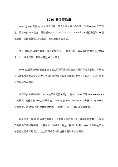
8086 晶体管数量
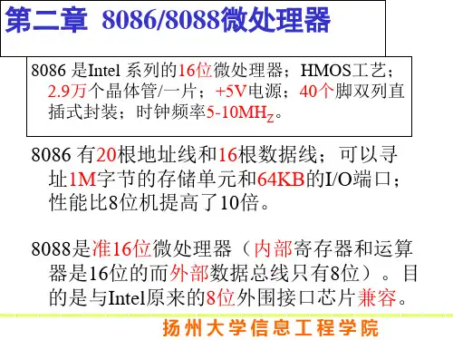
8086是Intel系列的16位微处理器,芯片上有4万个晶体管,采用HMOS工艺制造,用单一的+5V电源,时钟频率为4.77MHz~10MHz。
8086有16根数据线和20根地址线,它既能处理16位数据,也能处理8位数据。
关于8086的晶体管数量,有不同的说法。
一种说法称,其晶体管数量约为29000个;另一种说法称,其晶体管数量为4万个。
8086处理器的晶体管数量较多的主要原因是当时的计算需求和技术限制。
早期的个人计算机需要在处理大量的数据时能够提供较高的性能。
而为了实现这一目标,需要使用较多的晶体管。
与后来的处理器相比,8086的晶体管数量较少。
例如,1997年的Intel Pentium II (奔腾II)处理器有750万个晶体管,1999年的Intel Pentium III(奔腾III)有950万个晶体管,而2000年的Intel Pentium 4(奔腾4)则有4210万个晶体管。
综上所述,8086的晶体管数量是一个有争议的话题。
关于其确切的数量,不同的资料给出了不同的答案。
尽管如此,不可否认的是,在那个时期,8086处理器的晶体管数量已经相当可观了,这主要归功于当时的技术限制和计算需求。
8086-16位微处理器介绍第⼆章 8086/8088(16位)微处理器第⼀节、16位微处理器第⼀代微处理器 1971年Intel 公司推出4004和8008,是4和8位微处理器,采⽤PMOS ⼯艺。
第⼆代微处理器 1974年推出的8080、M6800、Z-80等,是8位微处理器,采⽤NMOS ⼯艺。
第三代微处理器 70年代后期Intel 公司推出8086/8088、Motorola 公司M68000、Zilog 公司的Z8000,是16位微处理器,采⽤HMOS ⼯艺。
80年代以来,Intel 公司推出80186⽤80286,与8086/8088兼容。
第四代微处理器 1985年,推出的80386及M68020是32位微处理器。
1989年推出80486。
1993年推出Pentium 及80586等更⾼性能的32位和64位微处理器。
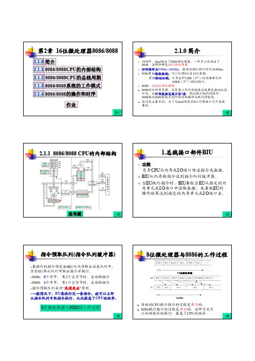
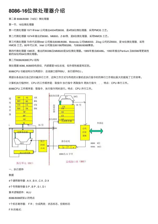
第⼆节8086/8088CPU 结构微处理器 8086, 8088结构类似,内部都是16位总线,但外部性能是有区别。
8086CPU 功能结构分为两部分:总线接⼝部件BIU ,执⾏部件EU 。
两部分各⾃执⾏⾃⼰的功能并⾏⼯作,这种⼯作⽅式与传统的计算机在执⾏指令时的串⾏⼯作相⽐极⼤的提⾼了⼯作效率。
计算机执⾏程序时,CPU 的⼯作顺序是:取指令执⾏指令再取指令再执⾏指令...特点:CPU 串⾏⼯作。
8086CPU ⼯作顺序是:取指令,执⾏指令同时进⾏。
特点:CPU 并⾏⼯作。
⼀、执⾏部件数据4个通⽤寄存器 : A X , B X , C X , D X4个专⽤寄存器 S P , B P , S I , D I算术逻辑部件:ALU8086/8088的EU 的特点1个标志寄存器: F R ;分成两类:状态标志、控制标志F R 的格式:⼆、总线接⼝部件BIU功能:负责与存储器、I/O 端⼝传送数据BIU 的组成:4个段地址寄存器(16位):CS 、DS 、ES 、SS16位指令指针寄存器IP20位地址加法器6字节的指令队列⼀条指令20地址的形成:由代码段CS 左移4位后与指令指针寄存器IP 内容相加得到注意:指令执⾏单元(EU )的功能:⼀般情况下,指令按照它存放的顺序先后执⾏,EU 源源不断地从指令队列中取得指令代码,达到满负荷地连续执⾏指令⽽省去“取指令”的时间。

观察8086最小模式下的总线读操作和写操作的过程,我们首先要了解8086处理器的基本结构和工作原理。
8086处理器是一种16位的微处理器,它具有20条位置区域总线和16条数据总线,采用小端模式存储数据。
在最小模式下,8086处理器通过最基本的方式与外部设备进行通信,即使用最小配置的控制信号和数据线。
这样的设计使得了解8086最小模式的总线读写操作成为首要的事情。
在8086最小模式下,总线读操作的过程可以简要概述为以下几个步骤:1. 位置区域提取当8086处理器需要进行读操作时,首先会将内存位置区域放置在位置区域总线上,由外部设备识别。
2. 存储器响应外部设备会根据位置区域总线上的位置区域信息,判断是否有存储器需要响应,如果有,则从数据总线上将数据传送给8086处理器。
3. 数据接收8086处理器将从数据总线上接收到的数据,存储到内部的数据寄存器中,以便后续的处理和使用。
而在8086最小模式下,总线写操作的过程则包括以下几个步骤:1. 位置区域提取与总线读操作类似,8086处理器在进行写操作时,也会将内存位置区域放置在位置区域总线上,以指明要写入数据的存储单元。
2. 数据发送8086处理器将要写入的数据放置在数据总线上,等待外部设备进行响应并接收数据。
3. 存储器响应外部设备接收到数据后,会根据位置区域总线上的位置区域信息,将数据存储到指定的存储单元中。
通过以上对8086最小模式下的总线读写操作过程的简要描述,我们可以初步了解到在最小配置下,8086处理器是如何通过位置区域总线和数据总线与外部设备进行读写操作的。
但要更深入地理解和掌握这些过程,我们需要更详细地了解8086处理器在总线读写操作过程中各种控制信号的使用,以及外部设备的响应方式和时序要求。
这涉及到了处理器的时序控制和总线控制,是非常复杂和深入的内容。
同时也需要深入了解8086处理器的寻址方式、存储器结构、数据传送方式等相关知识,以便更全面地理解总线读写操作的实际应用。

嵌入式微处理器的分类
什么是嵌入式微处理器?
嵌入式微处理器是一种由内置单片机的微型计算机,这种集成的单片机可以直接安装于普通的电子设备中,提供嵌入式控制功能,它们完全由软件来控制。
这些微处理器通常具有快速的处理能力,并带有嵌入式的外设,能够将计算机的功能植入到可移植设备当中,实现对多功能电子产品的整体控制。
嵌入式微处理器分类
嵌入式微处理器可以分为以下几种:
1、 8位微处理器:这类微处理器是8位指令操作的,数据宽度为8位,具有较少内存容量、低功耗、低成本和简单模块化的特点。
它们通常用于家用电器和自动控制中。
2、 16位微处理器:16位微处理器对指令有更高的处理能力,指令和数据均为16位,多用于工控系统、信号处理系统中,常用于多类型设备的自动化控制、软件开发等领域。
3、 32位微处理器:32位微处理器使用32位指令和数据宽度,它们更快、更强大,一般用于工业、商业、家用自动控制系统。
4、 64位微处理器:这类微处理器使用64位指令和数据宽度,具有极高的运算性能和网络数据处理能力,常用于图形处理、数字信号处理、科学计算以及各类嵌入式控制系统中。
- 1 -。
8086微处理器的指令集架构8086微处理器是一种16位的通用微处理器,由英特尔公司于1978年发布。
它的指令集架构称为x86,后来的许多处理器都是基于该架构进行扩展的。
这个指令集架构是8086微处理器与其后继处理器(如80286、80386等)之间的兼容性的基础,影响了后来的计算机硬件和软件设计。
8086指令集架构具有大量的指令和寻址模式,这些指令可以操作不同的数据类型和寄存器。
下面我们来介绍一些8086指令集的主要特点和功能:1.数据传送指令:- MOV:用于将数据从一个位置复制到另一个位置。
例如,MOV AX, BX可以将BX寄存器的内容复制到AX寄存器。
- PUSH和POP:用于将数据从寄存器或内存推送到堆栈或从堆栈中弹出。
例如,PUSH AX将AX寄存器的内容推送到堆栈中。
2.算术和逻辑指令:- ADD、SUB、INC和DEC:用于对寄存器或内存中的数据执行加法、减法、递增和递减操作。
- AND、OR、XOR和NOT:用于对寄存器或内存中的数据执行逻辑操作,如与、或、异或和取反。
- MUL和DIV:用于对寄存器或内存中的数据执行乘法和除法操作。
3.控制转移指令:- JMP:用于无条件跳转到指定标签或内存位置。
- JZ、JNZ、JE、JNE等:用于根据条件跳转到不同的指令位置。
例如,JZ表示如果零标志位为真,则跳转。
- CALL和RET:用于调用和返回子程序。
4.串操作指令:- MOVS、LODS、STOS、CMPS:用于在内存之间复制、加载、存储和比较数据。
- REP和REPE:用于重复执行串操作指令。
5.输入输出指令:- IN和OUT:用于从输入输出端口读取和写入数据。
- INT和IRET:用于进行中断和中断返回操作。
在8086指令集架构中,还有一些特殊的指令和寻址模式,用于实现更复杂的功能。
例如,8086支持段寻址模式,即使用段寄存器和偏移地址的组合来访问内存。
此外,还有一些面向特定任务的指令,如乘法指令和浮点操作指令等。
简述8086微处理器工作过程概述及解释说明1. 引言1.1 概述8086微处理器是Intel公司于1978年推出的一种16位微处理器。
它是英特尔80x86系列中的第一个成员,也是后来广泛应用的x86架构的基础。
通过对8086微处理器工作过程进行简要概述和解释说明,本文旨在帮助读者更好地理解这一经典微处理器的工作原理。
1.2 文章结构本文分为五个主要部分:引言、8086微处理器工作过程、8086微处理器的工作原理分析、8086微处理器的数据传输和操作方式以及结论。
在“引言”部分,将对文章整体进行概述,明确目标,并简要介绍该文各个部分的内容与主题重点.1.3 目的本文旨在提供有关8086微处理器工作过程的详细解释和说明,使读者了解其架构、指令执行流程、内部寄存器和指令集等关键信息。
此外,还将深入探讨8086微处理器的工作原理,包括数据总线与地址总线、控制信号和时序控制以及内部组成结构与功能模块等方面。
最后,文章还将重点介绍数据传输和操作方式,并回顾关键要点。
希望通过本文的阅读,读者能够对8086微处理器的工作过程有更全面、深入的理解,并为未来微处理器的发展做出贡献。
这是引言部分的相关内容,请按照这个框架进行详细撰写。
2. 8086微处理器工作过程:2.1 架构概述:8086微处理器是Intel公司于1978年推出的一款16位微处理器。
它采用复杂指令集计算机(CISC)架构,具有数据总线宽度为16位,地址总线宽度为20位,并拥有14个16位寄存器。
该处理器运行在最大频率为5 MHz的时钟速度下,可以执行多达290,000条指令每秒。
2.2 指令执行流程:8086微处理器的指令执行流程可以分为取指、译码、执行和写回四个阶段。
首先,从内存中读取指令并将其存储在指令寄存器中;然后,译码单元将指令解码成相应的操作,并从内存或寄存器中获取操作数;接下来,在算术逻辑单元(ALU)中进行运算或逻辑操作;最后,将结果写回到寄存器或内存中。
8086的应用及原理图一、简介8086是由英特尔(Intel)公司于1978年推出的一款16位微处理器。
它成为了后续x86架构的基础,并且在80年代和90年代广泛应用于各种个人电脑和工作站中。
二、8086的应用8086微处理器在各个领域有着广泛的应用,以下是一些常见的应用场景:1.个人电脑:8086是最早的一种个人电脑用微处理器。
在80年代和90年代,它极大地推动了个人电脑的发展,成为了当时最主流的处理器。
2.工业控制:8086在工业控制系统中也被广泛使用。
由于其较高的计算能力和稳定性,能够处理复杂的算法和控制逻辑,因此在自动化生产线、仪器仪表和机械设备等方面有着重要的应用。
3.嵌入式系统:由于8086具有较小的体积和低功耗的特点,使得它在嵌入式系统中有广泛的应用。
像医疗设备、智能家居和智能穿戴设备等嵌入式系统中,8086可以负责控制和处理各种传感器和设备。
4.航空航天:8086在航空航天领域有着重要的作用。
由于其高可靠性和强大的计算能力,使得它被广泛应用于火箭控制系统、卫星通信和导航系统等方面。
三、8086的原理图1. 存储器单元•内部存储器:用于存放指令和数据,包括寄存器和内存。
–寄存器:包括通用寄存器、指令指针寄存器、段寄存器等。
–内存:分为代码段、数据段和堆栈段等。
2. 控制单元•指令寄存器(IR):用于存放当前执行的指令。
•程序计数器(PC):存放指令的地址。
•指令译码器:将指令解码为对应的操作。
•控制逻辑:根据指令执行的需求,控制各个模块的工作。
3. 算术逻辑单元•运算器:负责执行各种算术运算和逻辑运算。
•标志寄存器(FLAGS):状态寄存器,记录运算结果中的状态。
4. 输入输出单元•输入端口:负责接收外部设备的数据。
•输出端口:负责将数据发送给外部设备。
四、总结8086微处理器作为早期个人电脑使用的重要组成部分,对计算机技术的发展有着深远的影响。
它在个人电脑、工业控制、嵌入式系统和航空航天等领域有着广泛的应用。
8086/8088微处理器8086是全16位微处理器,内、外数据总线都是16位。
8088是准16位微处理器,内数据总线是16位,外数据总线是8位。
二者除外数据总线位数及与此相关的部分逻辑稍有差别外,内部结构和基本性能相同,指令系统完全兼容。
1. 内部结构8086/8088微处理器从功能上可分为两个独立的处理单元:执行单元EU(Execution Unit)和总线接口单元BIU(Bus Interface Unit)。
其内部结构如图2.1所示。
执行单元EU由8个16位的通用寄存器、1个16位的标志寄存器、1个16位的暂存寄存器、1个16位的算术逻辑单元ALU及EU控制电路组成。
8个通用寄存器中,AX、BX、CX、DX为数据寄存器,用于存放参与运算的数据或运算的结果,它们中的每一个既可以作为一个16位寄存器使用,又可以将高、低8位分别作为两个独立的8位寄存器使用。
作为8位寄存器时,它们的名称分别为AL、AH、BL、BH、CL、CH、DL、DH。
这些寄存器除了用作通用寄存器外,通常还有各自特殊的用法: AX作累加器,所有的I/O指令及一部分串操作必须使用AX或AL来执行,另外还有一些指令使用AX及由AX 分出的AL、AH作为缺省的操作数,如乘、除法指令;BX作基址寄存器,在计算内存地址时,常用于存放基址;CX作计数寄存器,可以在循环、重复的串操作及移位操作中被作为计数器来使用;DX作数据寄存器,在一些I/O指令中用来保存端口地址。
指针寄存器SP和BP分别为堆栈指针寄存器和基址指针寄存器,作为通用寄存器的一种,它们可以存放数据,但实际上,它们更经常、更重要的用途是存放内存单元的偏移地址。
而变址寄存器DI和SI则主要用于变址寻址方式的目的变址和源变址。
图2.1 8086/8088CPU内部结构示意图总线接口单元BIU由4个16位的段寄存器(CS、SS、DS、ES)、1个16位的指令指针寄存器IP、1个与EU通信的内部暂存器、1个指令队列、1个计算20位物理地址的地址加法器∑及总线控制电路组成。