irfh5010规格书
- 格式:pdf
- 大小:283.21 KB
- 文档页数:8

Single wire LGY/H05V - K 2,50mm2 50m Color: BlackThe offered wire has a flexible, multi-strand conductor with a cross-section of2,50 mm2 insulated with new generation polyvinite PVC. Thanks to its outstanding performance, it is a great choice for any professional who relies on excellent quality, reliability and convenience of use. This flexible, well-laying, resistant to surrounding conditions and user-oriented product is ideal for even the most advanced production projects and any assembly, service and hobby work.Wire technical parameters :Product normative classification LGY/H05V-K PRO SeriesThe rated cross-section of the conductor 2,50mm2Wire cross-section in AWG AWG 14Manufacturer part number BQ MPN LGY2.5-BKStructure of twisted multi-wire conductor 50 x ∅ 0,25mmConstruction of conductor Regularly twisted strandConductor material Copper CuConductor resistance at T=20o C max.7,6 ÷ min. 7,0 mΩ/mInsulating material Modified polyvinite PVCOuter diameter of wire ∅ 3,0mm ± 0,05Type of color insulation Plain colorWire insulation color and RAL number RAL 9005BlackApproximate net weight of wire 27,2 kg/kmCopper index – conductor net weight 24,0 kg/kmResistance to vibration, oscilation, overload YESResistance to lubricants and chemical agents YESResistance to flame spreading YES – Self extinguishing typeMethod of electrical assembly and connecting Crimping, Soldering, TwistingPermissible current load of the cable 20,6 A (max. 25 A)Long-term current capacity of the cable 10,9 AMaximum cable operating voltage 500 VBreakdown voltage of the insulation > 10kVOperating temperature range of the cable -40o C÷+105o C (max. +120o C)Section in packaging 50 metersApproximate gross weight of the package 1,46 kgPackaging - way of wire confection Evenly winded onto a spoolPackaging material and dimensions - spools ABS = 132mm / H = 57mmPackaging logistical security Thermo-shrinkable POF film coverWe guarantee constant availability of items in stock and immediate shipping! Single wires LGY 300V/500V / H05V-K with BQ logo guarantee not only the highest global product quality and the latest technologies of workmanship taking into account environmental protection, but also provide convenience of usage and savings coming from reliability. Thanks to the use of highest quality copper, with specifically raised pureness in our regularly twisted strands with cross sections of 0,35mm2, 0,50mm2, 0,75mm2, 1,00mm2, 1,50mm2 and 2,50mm2 and their regularity, LGY/H05V-K wires provided by BQ guarantee almost lossless transmission of sent signal or current, significant facilitation of soldered and crimped assembly, resistance to vibration and oscillation and outstanding pliability and flexibility.BQ new generation of modified polyvinite insulation is specially thinned to guarantee a smaller outer diameter of the wire at the same cross-section of the conductive vein with holding all dielectric parameters and operating voltage of up to 500V. This allows for better planning of electrical harnesses and more efficient use of cable glands. This is possible thanks to the increased physicochemical properties of insulation, which further makes offered wires perfectly cope with the surrounding conditions and aggressive chemical agents. The insulation is extremely smooth and glossy, is not absorbent, does not harden and does not crumble, and allows an unprecedented operating temperature in the range of -40°C to +105°C(max +120°C). This increased thermal range also reduces installation time and significantly decreases the risk of insulation melting when making high-current soldered connections or encapsulating connections with shrink pipes.A very wide range of plain colors insulation and hudge range of two-color variety types in the form of a base color and marker stripe significantly save on wire marking systems in multi-wire harnesses, eliminate the need for cable markers and allow quick identification of a given wire along the entire length of the harness, even in hard-to-reach places. The cables are supplied in sections of 200m, 100m or 50m depending on the cross section of the wire, and winded onto a fully recyclable, comfortable-to-use spool with diameter of Ø = 132mm with internal guide hole Ø = 26mm, which allows you to increase the comfort of work, ending the problem with finding the end of the wire or laborious untangling after uncontrolled expansion. It greatly accelerates and facilitates the execution of multi-wire harnesses, because it is enough to put spools with a set number of wires on one guide rod and pull them all together and, as you develop, connect them into a bundle with the appropriate electrical tape, self-clamping bands or passing them through the corrugated conduit. BQ equip all spools with test seals to help you quickly find the beginning of the cable section and pack them in a sealed cover made of transparent shrink film, which allows you to quickly find the necessary color on the shelf of the warehouse, protects insulation from oxidation, dust or getting dirty during storage and alwaysguarantees the final recipient the highest quality of the cables when removed from the package.The parameters of the cables meet the requirements of ISO 9001, ISO 14001, PN-87/E-90054 (Polish standard), VDE (German standard), BASEC (UK standard), are authorized for use on EU markets (73/23/EEC standard) and CE marked (Directive 2006/95/EC), and comply with environmental directives RoHS(Act 2002/95/EU), RoHS-2(Act 2011/65/EU), RoHS-3(Act 2015/863) and comply with REACH environmental requirements (Regulation 1907/2006). According to EN 60332-1-2, the cables are Eca grade, do not spread flame and are approved for usage in construction works.At each request of the Recipient, we issue a certificate of conformity free of charge.Offered single wires are universally applicable thanks to their professional design & performance and are ideal for most manufacturing, service or hobby projects in all areas of electronics and electrical engineering. They are most oftenly used in industrial and electromedical automation, automotive industry, cranes, lighting, construction of all kinds of devices from alarms, scales, arcade machines or sunbeds to advanced technological lines, when making power lines, steering, control, executive installations, on-board installations, alarms and many other applications. They are also often used in the manufacture, modernization, modification or reconstruction of all types of vehicles: electric scooters and electric skateboards, mopeds, motorbikes, quads, buggies, cars and trucks, special vehicles (taxis, ambulances, fire trucks, cranes, tow trucks, loading lifts etc.), buses, tractors, semi-trailers, trailers, trams, trains, and they can be found even on inland yachts and speedboats, powered hang gliders or sailplanes. They are also oftenly used to control and power energy-efficient LED lighting systems, connect computer controllers to receivers, implement smart building projects, and for any service and hobby work.LGY/H05V-K wires provided by BQ are an excellent solution for any professional who values quality and convenience of use in wires. The use of these wires is simple, fast, economical and guarantees perfect reliability.。
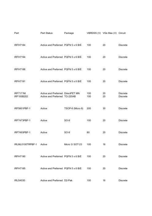
Part Part Status Package VBRDSS (V)VGs Max (V)Circuit IRFH7184Active and Preferred PQFN 5 x 6 B/E10020Discrete IRFH7194Active and Preferred PQFN 5 x 6 B/E10020Discrete IRFH7188Active and Preferred PQFN 5 x 6 B/E10020Discrete IRFH7191Active and Preferred PQFN 5 x 6 B/E10020Discrete IRF7171M Active and Preferred DirectFET MN10020Discrete IRF100B202Active and Preferred TO-220AB10020Discrete IRF5801PBF-1Active TSOP-6 (Micro 6)20030Discrete IRF7473PBF-1Active SO-810020Discrete IRF7493PBF-1Active SO-88020Discrete IRLML0100TRPBF-1Active Micro 3/ SOT-2310016Discrete IRFH7190Active and Preferred PQFN 5 x 6 B/E10020Discrete IRFH7185Active and Preferred PQFN 5 x 6 B/E10020Discrete IRLS4030Active and Preferred D2-Pak10016Discrete IRFHM3911Active and Preferred PQFN 3.3 x 3.310020Discrete IRFS4321-7P Active and Preferred D2-Pak 7-Lead15030Discrete IRF3315S Active D2-Pak15020Discrete IRF3610S Active and Preferred D2-Pak10020Discrete IRFS4321Active and Preferred D2-Pak15030Discrete IRFS23N15D Active D2-Pak15030Discrete IRFS4510Active and Preferred D2-Pak10020Discrete IRFS4610Active D2-Pak10020Discrete IRFS52N15D Active D2-Pak15030Discrete IRFS38N20D Active D2-Pak20030Discrete IRFS4010Active and Preferred D2-Pak10020Discrete IRFS4115Active and Preferred D2-Pak15020Discrete IRF7769L1Active and Preferred DirectFET L810020Discrete IRFP4868Active and Preferred TO-247AC30020Discrete IRFP4137Active and Preferred TO-247AC30020Discrete IRFB4137Active and Preferred TO-220AB30020Discrete IRF7820Active and Preferred SO-820020Discrete IRLS4030-7P Active and Preferred D2-Pak 7-Lead10016Discrete IRFS4115-7P Active and Preferred D2-Pak 7-Lead15020Discrete IRFH7110Active and Preferred PQFN 5 x 6 B/E10020Discrete IRFR825Active and Preferred D-Pak50020Discrete IRFR812Active and Preferred D-Pak50020Discrete IRFR4510Active and Preferred D-Pak10020Discrete IRFB4510Active and Preferred TO-220AB10020Discrete IRFSL4510Active and Preferred TO-26210020Discrete IRFB812Active and Preferred TO-220AB50020Discrete IRLU120N Active I-Pak10016Discrete IRFU120N Active I-Pak10020Discrete IRLU3110Z Active and Preferred I-Pak10016Discrete IRF3710L Active TO-26210020Discrete IRFU3910Active I-Pak10020Discrete IRLU3410Active I-Pak10016Discrete IRFU4510Active and Preferred I-Pak10020Discrete IRFU220N Active I-Pak20020Discrete IRFU3710Z Active and Preferred I-Pak10020Discrete IRFU13N20D Active I-Pak20030Discrete IRFU4620Active and Preferred I-Pak20020DiscreteIRFU4615Active and Preferred I-Pak15020Discrete IRFH5220Active and Preferred PQFN 5 x 6 B/E20020Discrete IRFH5215Active and Preferred PQFN 5 x 6 B/E15020Discrete IRFH5025Active and Preferred PQFN 5 x 6 B/E25020Discrete IRFH5210Active and Preferred PQFN 5 x 6 B/E10020Discrete IRFH5010Active and Preferred PQFN 5 x 6 B/E10020Discrete IRFI4410Z Active and Preferred TO-220 FullPak (Iso)10030Discrete IRFH5110Active and Preferred PQFN 5 x 6 B/E10020Discrete IRFP150M Active and Preferred TO-247AC10020Discrete IRFP260M Active and Preferred TO-247AC20020Discrete IRFP250M Active and Preferred TO-247AC20020Discrete IRFS4227Active and Preferred D2-Pak20030Discrete IRLH5030Active and Preferred PQFN 5 x 6 B/E10016Discrete IRFH5015Active and Preferred PQFN 5 x 6 B/E15020Discrete IRF7815Active and Preferred SO-815020Discrete IRLML0100Active and Preferred Micro 3/ SOT-2310016Discrete IRF7779L2Active and Preferred DirectFET L815020Discrete IRFH5020Active and Preferred PQFN 5 x 6 B/E20020Discrete IRF7799L2Active and Preferred DirectFET L825030Discrete IRF7665S2Active and Preferred DirectFET SB10020Discrete IRFS4020Active and Preferred D2-Pak20020Discrete IRFSL4020Active and Preferred TO-26220020Discrete IRFH5053Active PQFN 5 x 6 A10020Discrete IRFP4768Active and Preferred TO-247AC25020Discrete IRLSL4030Active and Preferred TO-26210016Discrete IRLB4030Active and Preferred TO-220AB10016Discrete IRFS4620Active and Preferred D2-Pak20020Discrete IRFS5615Active and Preferred D2-Pak15020Discrete IRFR4615Active and Preferred D-Pak15020Discrete IRFR4620Active and Preferred D-Pak20020Discrete IRFS4615Active and Preferred D2-Pak15020Discrete IRFB4115Active and Preferred TO-220AB15020Discrete IRFS4310Z Active and Preferred D2-Pak10020Discrete IRLR2908Active D-Pak8016Discrete IRFSL4115Active and Preferred TO-26215020Discrete IRFS4010-7P Active and Preferred D2-Pak 7-Lead10020Discrete IRFSL4010Active and Preferred TO-26210020Discrete IRFS4127Active and Preferred D2-Pak20020Discrete IRFS4229Active and Preferred D2-Pak25030Discrete IRFP4668Active and Preferred TO-247AC20030Discrete IRFP4568Active and Preferred TO-247AC15030Discrete IRFB4615Active and Preferred TO-220AB15020Discrete IRFB5620Active and Preferred TO-220AB20020Discrete IRFB5615Active and Preferred TO-220AB15020Discrete IRFB4620Active and Preferred TO-220AB20020Discrete IRFB4127Active and Preferred TO-220AB20020Discrete IRFP4468Active and Preferred TO-247AC10020Discrete IRFR3410Active D-Pak10020Discrete IRFR540Z Active D-Pak10020Discrete IRFP4110Active and Preferred TO-247AC10020Discrete IRFP4410Z Active and Preferred TO-247AC10020DiscreteIRFP4310Z Active and Preferred TO-247AC10020Discrete IRFS4310Active D2-Pak10020Discrete IRFS4410Active D2-Pak10020Discrete IRF6655Active and Preferred DirectFET SH10020Discrete IRLR3110Z Active and Preferred D-Pak10016Discrete IRFSL4227Active TO-26220030Discrete IRFS4410Z Active and Preferred D2-Pak10020Discrete IRF6785Active and Preferred DirectFET MZ20020Discrete IRF6775M Active and Preferred DirectFET MZ15020Discrete IRFSL4310Z Active TO-26210020Discrete IRFB4310Z Active and Preferred TO-220AB10020Discrete IRFB4410Z Active and Preferred TO-220AB10020Discrete IRFSL4410Z Active TO-26210020Discrete IRF6643Active and Preferred DirectFET MZ15020Discrete IRF6641Active and Preferred DirectFET MZ20020Discrete IRF6662Active and Preferred DirectFET MZ10020Discrete IRF6668Active and Preferred DirectFET MZ8020Discrete IRF6665Active and Preferred DirectFET SH10020Discrete IRFI4321Active TO-220 FullPak (Iso)15030Discrete IRFP4321Active and Preferred TO-247AC15030Discrete IRFB4321Active and Preferred TO-220AB15030Discrete IRFSL4321Active TO-26215030Discrete IRF6646Active and Preferred DirectFET MN8020Discrete IRFP4332Active and Preferred TO-247AC25030Discrete IRFB4332Active and Preferred TO-220AB25030Discrete IRF6644Active and Preferred DirectFET MN10020Discrete IRF6645Active and Preferred DirectFET SJ10020Discrete IRFI4229Active TO-220 FullPak (Iso)25030Discrete IRFB4229Active and Preferred TO-220AB25030Discrete IRFP4229Active and Preferred TO-247AC25030Discrete IRFB4020Active and Preferred TO-220AB20020Discrete IRFB4019Active and Preferred TO-220AB15020Discrete IRF3710ZS Active D2-Pak10020Discrete IRFP4227Active and Preferred TO-247AC20030Discrete IRF7854Active and Preferred SO-88020Discrete IRF7853Active and Preferred SO-810020Discrete IRF8010S Active and Preferred D2-Pak10020Discrete IRFB4110Active and Preferred TO-220AB10020Discrete IRFB4227Active and Preferred TO-220AB20030Discrete IRFI4227Active TO-220 FullPak (Iso)20030Discrete IRF5802Active TSOP-6 (Micro 6)15030Discrete IRF5801Active TSOP-6 (Micro 6)20030Discrete IRFSL4310Active TO-26210020Discrete IRFSL38N20D Active TO-26220030Discrete IRF7493Active and Preferred SO-88020Discrete IRF7495Active and Preferred SO-810020Discrete IRFB4212Active and Preferred TO-220AB10020Discrete IRFB4310Active TO-220AB10020Discrete IRF530NS Active D2-Pak10020Discrete IRL540NS Active and Preferred D2-Pak10016Discrete IRFR9N20D Active D-Pak20030DiscreteIRF3710S Active D2-Pak10020Discrete IRL520NS Active and Preferred D2-Pak10016Discrete IRF7452Active SO-810030Discrete IRF630NS Active D2-Pak20020Discrete IRLR3410Active and Preferred D-Pak10016Discrete IRFR120N Active D-Pak10020Discrete IRFR13N15D Active D-Pak15030Discrete IRL2910S Active and Preferred D2-Pak10016Discrete IRF7451Active SO-815030Discrete IRFR13N20D Active D-Pak20030Discrete IRLR120N Active and Preferred D-Pak10016Discrete IRF640NS Active D2-Pak20020Discrete IRL530NS Active and Preferred D2-Pak10020Discrete IRF540NS Active D2-Pak10020Discrete IRF3415S Active D2-Pak15020Discrete IRFS59N10D Active D2-Pak10030Discrete IRFR3518Active D-Pak8020Discrete IRF1310NS Active D2-Pak10020Discrete IRFR220N Active D-Pak20020Discrete IRFR18N15D Active D-Pak15030Discrete IRF7490Active SO-810020Discrete IRFL4315Active SOT-22315030Discrete IRFS31N20D Active D2-Pak20030Discrete IRFR120Z Active and Preferred D-Pak10020Discrete IRFR3910Active D-Pak10020Discrete IRF520NS Active D2-Pak10020Discrete IRF540ZS Active D2-Pak10020Discrete IRFS41N15D Active D2-Pak15030Discrete IRFS23N20D Active D2-Pak20030Discrete IRF7450Active SO-820030Discrete IRF7473Active SO-810020Discrete IRF7488Active SO-88020Discrete IRFL4310Active SOT-22310020Discrete IRFS33N15D Active D2-Pak15030Discrete IRF7465Active SO-815030Discrete IRFR3710Z Active D-Pak10020Discrete IRFB4410Active TO-220AB10020Discrete IRFB4610Active and Preferred TO-220AB10020Discrete IRFBA90N20D Active Super 220 (TO-273AA)20030Discrete IRFPS3815Active Super 247 (TO-274AA)15030Discrete IRFPS3810Active Super 247 (TO-274AA)10030Discrete IRF1310N Active TO-220AB10020Discrete IRFB38N20D Active TO-220AB20030Discrete IRF520N Active TO-220AB10020Discrete IRL520N Active and Preferred TO-220AB10016Discrete IRFP140N Active TO-247AC10020Discrete IRFB61N15D Active TO-220AB15030Discrete IRFP90N20D Active TO-247AC20030Discrete IRF540ZL Active TO-26210020Discrete IRLI530N Active TO-220 FullPak (Iso)10016Discrete IRLI2910Active TO-220 FullPak (Iso)10016DiscreteIRFB33N15D Active TO-220AB15030Discrete IRFB23N20D Active TO-220AB20030Discrete IRF8010Active and Preferred TO-220AB10020Discrete IRFP3415Active TO-247AC15020Discrete IRFB42N20D Active TO-220AB20030Discrete IRFU3410Active I-Pak10020Discrete IRFB260N Active TO-220AB20020Discrete IRLI540N Active TO-220 FullPak (Iso)10016Discrete IRF3710Z Active TO-220AB10020Discrete IRF3710ZL Active TO-26210020Discrete IRL530N Active and Preferred TO-220AB10016Discrete IRFR3411Active and Preferred D-Pak10020Discrete IRFR24N15D Active D-Pak15030Discrete IRFI530N Active TO-220 FullPak (Iso)10020Discrete IRFR15N20D Active D-Pak20030Discrete IRFB59N10D Active TO-220AB10030Discrete IRF540NL Active TO-26210020Discrete IRF630N Active TO-220AB20020Discrete IRFB31N20D Active TO-220AB20030Discrete IRF640NL Active TO-26220020Discrete IRF640N Active TO-220AB20020Discrete IRFP3710Active and Preferred TO-247AC10020Discrete IRLI520N Active TO-220 FullPak (Iso)10016Discrete IRFP4710Active TO-247AC10020Discrete IRFP150N Active TO-247AC10020Discrete IRL2910Active and Preferred TO-220AB10016Discrete IRL540N Active and Preferred TO-220AB10016Discrete IRFP260N Active TO-247AC20020Discrete IRFP250N Active TO-247AC20020Discrete IRF530N Active TO-220AB10020Discrete IRF3415Active TO-220AB15020Discrete IRFB4710Active TO-220AB10020Discrete IRF3710Active TO-220AB10020Discrete IRFB41N15D Active TO-220AB15030Discrete IRFB23N15D Active TO-220AB15030Discrete IRFIB41N15D Active TO-220 FullPak (Iso)15030Discrete IRFI1310N Active TO-220 FullPak (Iso)10020Discrete IRF3315Active TO-220AB15020Discrete IRF540Z Active TO-220AB10020Discrete IRFI540N Active TO-220 FullPak (Iso)10020Discrete IRFB52N15D Active TO-220AB15030Discrete IRF540N Active TO-220AB10020Discrete IRFY240Active TO-257AA20020Discrete IRFY140Active TO-257AA10020Discrete IRFY130Active TO-257AA10020DiscreteRDS(on) Max 10V (mOhms)Qg Typ (nC)ID @ TC = 25C (A)Power Dissipation @ TC = 25C (W) 4.83612815616.4133539633105132826801046.536931048.677972212.23.926.06115.035220.0 2.57.526821045.236.01231604.387.0180370115.017.0112914.771.08635082.063.3219411.6100.010333315.071.08333090.037.023 3.813.958.06114014.090.07319032.060.06032054.060.0443204.7143.018037512.177.0993753.5200.012412532.0180.07051769.083.03834169.083.03834178.029.03.993.019037011.873.010538013.558.0581041300.022.7 6.01192200.013.3 3.67813.954.06314313.558.06214013.958.0611402200.013.3 3.67818513.3 6.93921016.7 5.8391434451402386.74020011529.39.55210522.79.55213.9544514360015 3.543186939140235259.5110782517144422624144 99.920.02058.020.027104 100.037.03214.939.055104 9.065.0100250 9.381.04347 12.448.063114 36.073.342160 40.0156.050300 75.082.030214 26.070.062330 9.044.031.033.056250 43.025.0220.0 2.511.097.067125 55.036.04338.0110.035125 62.08.314.430 105.018.018100 105.018.018100 18.024.04617.5180.093520 4.387.0180370 4.387.0180370 78.025.024144 42.026.033144 42.026.033144 78.025.024144 42.026.033144 11.077.0104380 6.0120.0127250 28.022.039120 12.177.099375 4.0150.0190380 4.7143.0180375 22.0100.072375 4872.045330 9.7161.0130520 5.9151.0171517 39.026.035144 72.525.025144 39.026.035144 72.525.025144 20.0100.076375 2.6360.0290520 39.037.031110 28.539.03591 4.5150.0180370 9.083.0972306.0120.01342807.0170.0140330 10.0120.096250 62.08.742 14.034.063140 26.070.062330 9.083.097230 100.026.01957 56.025.02889 6.0120.0127250 6.0120.0127250 9.083.097230 9.083.097230 34.539.089 59.934.089 22.022.089 15.022.05589 62.08.742 16.073.03446 15.571.078310 15.071.083330 15.071.083330 9.536.089 33.099.057360 33.099.060390 13.035.089 35.014.042 46.073.01946 46.072.046330 46.072.044310 100.018.018100 95.013.01780 18.082.059160 25.070.065330 13.427.018.028.015.081.080260 4.5150.0180370 26.070.065190 22.073.02618 1200.0 4.5 2.0 2200.0 3.90.6 2.0 7.0170.0140330 54.060.044320 15.031.022.034.072.515.01860 7.0170.0130300 90.024.717 3.8 44.049.336 3.8 380.018.09.48623.086.757 3.8 180.013.310 3.8 60.033.0300.023.39.582 105.022.71552 210.016.79.139 180.019.01486 26.093.355 3.8 90.028.0235.025.014110 185.013.31139 150.044.718150 100.022.717 3.8 44.047.333 3.8 42.0133.343 3.8 25.076.059200 29.037.038110 36.073.342 3.8 600.015.0543 125.028.018110 39.037.0185.012.082.070.031200 190.0 6.98.735 115.029.31552 200.016.79.547 26.542.03692 45.072.041200 100.057.024170 170.026.026.061.029.038.0200.017.056.060.033 3.8 280.010.018.069.056140 10.0120.096250 14.090.073190 23.0160.098650 15.0260.0105441 9.0260.0141441 36.073.342160 54.060.044320 200.016.79.748 180.013.31048 52.062.72794 32.095.060330 23.0180.094580 26.542.03692 100.022.71133 26.093.3274856.060.033 3.8 100.057.024170 15.081.080260 42.0133.343200 55.091.042.630039.037.03111040.0150.056380 44.049.32042 18.082.059160 18.082.059160 100.022.71779 44.048.032130 95.030.024140 110.029.31133 165.027.017140 25.076.059200 44.047.333140 300.023.39.582 82.070.031200 150.044.718150 150.044.718150 25.066.751180 180.013.37.727 14.0110.072190 36.073.339140 26.093.348200 44.049.336140 40.0156.049300 75.082.030214 90.024.71779 42.0133.343200 14.0110.075200 23.086.757200 45.072.041200 90.037.023 3.8 45.072.041200 36.080.02245 70.063.32194 26.542.03692 52.062.71842 32.060.060320 44.047.333140 180.040.010.277.039.316100 180.019.09.1Rth(JC) (K/W)Qual Level MSL Package Class0.8Industrial1Surface Mount without Leads 3.2Industrial1Surface Mount without Leads0.95Industrial1Surface Mount without Leads1.2Industrial1Surface Mount without Leads 1.2Industrial Surface Mount Can - DirectFET 0.68Industrial Thru-Hole62.5 (JA)Industrial1Surface Mount with Leads50 (JA)Industrial1Surface Mount with Leads50 (JA)Industrial1Surface Mount with Leads100 (JA)Surface Mount with Leads1.2Industrial1Surface Mount without Leads 0.80Industrial1Surface Mount without Leads 0.40Industrial1Surface Mount with Leads4.3Industrial1Surface Mount with Leads0.43Industrial1Surface Mount with Leads1.6Industrial1Surface Mount with Leads0.50Industrial1Surface Mount with Leads0.45Industrial1Surface Mount with Leads1.1Industrial1Surface Mount with Leads1.05Industrial1Surface Mount with Leads0.77Industrial1Surface Mount with Leads0.47Industrial1Surface Mount with Leads0.47Industrial1Surface Mount with Leads0.40Industrial1Surface Mount with Leads0.40Industrial1Surface Mount with Leads45 (JA)Industrial1Surface Mount Can - DirectFET 0.29Industrial Thru-Hole0.44Industrial Thru-Hole0.44Industrial Thru-Hole50 (JA)Industrial1Surface Mount with Leads0.40Industrial1Surface Mount with Leads0.40Industrial1Surface Mount with Leads1.2Industrial1Surface Mount without Leads 1.05Industrial1Surface Mount with Leads1.6Industrial1Surface Mount with Leads1.05Industrial1Surface Mount with Leads1.05Industrial Thru-Hole1.05Industrial Thru-Hole1.6Industrial Thru-Hole3.2Industrial Thru-Hole3.2Industrial Thru-Hole1.05Industrial Thru-Hole0.75Industrial Thru-Hole2.4Industrial Thru-Hole2.4Industrial Thru-Hole1.05Industrial Thru-Hole3.5Industrial Thru-Hole1.05Industrial Thru-Hole1.4Industrial Thru-Hole1.045Industrial Thru-Hole1.045Industrial Thru-Hole1.2Industrial1Surface Mount without Leads 1.2Industrial1Surface Mount without Leads0.50Industrial1Surface Mount without Leads1.2Industrial1Surface Mount without Leads 0.50Industrial1Surface Mount without Leads 3.2Industrial Thru-Hole1.1Industrial1Surface Mount without Leads 0.95Industrial Thru-Hole0.50Industrial Thru-Hole0.70Industrial Thru-Hole0.45Industrial1Surface Mount with Leads0.50Industrial1Surface Mount without Leads 0.50Industrial1Surface Mount without Leads 50 (JA)Industrial1Surface Mount with Leads100 (JA)Consumer1Surface Mount with Leads1.2Industrial1Surface Mount Can - DirectFET0.50Industrial1Surface Mount without Leads1.2Industrial1Surface Mount Can - DirectFET 62.5 (JA)Industrial1Surface Mount Can - DirectFET 1.43Industrial1Surface Mount with Leads1.43Industrial Thru-Hole1.6Consumer2Surface Mount without Leads 0.29Industrial Thru-Hole0.40Industrial Thru-Hole0.40Industrial Thru-Hole1.045Industrial1Surface Mount with Leads1.045Industrial1Surface Mount with Leads1.045Industrial1Surface Mount with Leads1.045Industrial1Surface Mount with Leads1.045Industrial1Surface Mount with Leads0.40Industrial Thru-Hole0.60Industrial1Surface Mount with Leads1.3Industrial1Surface Mount with Leads0.40Industrial Thru-Hole0.40Industrial1Surface Mount with Leads0.40Industrial Thru-Hole0.40Industrial1Surface Mount with Leads0.45Industrial1Surface Mount with Leads0.29Industrial Thru-Hole0.29Industrial Thru-Hole1.04Industrial Thru-Hole1.04Industrial Thru-Hole1.04Industrial Thru-Hole1.04Industrial Thru-Hole0.40Industrial Thru-Hole0.29Industrial Thru-Hole1.4Industrial1Surface Mount with Leads1.64Industrial1Surface Mount with Leads0.40Industrial Thru-Hole0.65Industrial Thru-Hole0.54Industrial Thru-Hole0.45Industrial1Surface Mount with Leads0.61Industrial1Surface Mount with Leads3.0Consumer1Surface Mount Can - DirectFET 1.05Industrial1Surface Mount with Leads0.45Industrial Thru-Hole0.65Industrial1Surface Mount with Leads1.4Consumer1Surface Mount Can - DirectFET 1.4Consumer1Surface Mount Can - DirectFET 0.60Industrial Thru-Hole0.60Industrial Thru-Hole0.65Industrial Thru-Hole0.65Industrial Thru-Hole1.4Consumer1Surface Mount Can - DirectFET 1.4Consumer1Surface Mount Can - DirectFET 1.4Consumer1Surface Mount Can - DirectFET 1.4Consumer1Surface Mount Can - DirectFET 3.0Consumer1Surface Mount Can - DirectFET2.73Industrial Thru-Hole0.49Industrial Thru-Hole0.45Industrial Thru-Hole0.45Industrial Thru-Hole1.4Consumer1Surface Mount Can - DirectFET 0.42Industrial Thru-Hole0.38Industrial Thru-Hole1.4Consumer1Surface Mount Can - DirectFET 3.0Consumer1Surface Mount Can - DirectFET2.73Industrial Thru-Hole0.45Industrial Thru-Hole0.49Industrial Thru-Hole1.43Industrial Thru-Hole1.88Consumer Thru-Hole0.92Industrial1Surface Mount with Leads0.45Industrial Thru-Hole50 (JA)Industrial1Surface Mount with Leads50 (JA)Industrial1Surface Mount with Leads0.57Industrial1Surface Mount with Leads0.40Industrial Thru-Hole0.45Industrial Thru-Hole0.45Industrial Thru-Hole62.5 (JA)Consumer1Surface Mount with Leads 62.5 (JA)Consumer1Surface Mount with Leads0.45Industrial Thru-Hole0.47Industrial Thru-Hole50 (JA)Consumer1Surface Mount with Leads50 (JA)Consumer1Surface Mount with Leads2.5Industrial Thru-Hole0.45Industrial Thru-Hole1.9Industrial1Surface Mount with Leads1.1Industrial1Surface Mount with Leads1.75Industrial1Surface Mount with Leads0.75Industrial1Surface Mount with Leads 3.1Industrial1Surface Mount with Leads 50 (JA)Consumer1Surface Mount with Leads1.83Industrial1Surface Mount with Leads2.4Industrial1Surface Mount with Leads3.2Industrial1Surface Mount with Leads 1.75Industrial1Surface Mount with Leads 0.75Industrial1Surface Mount with Leads 50 (JA)Consumer1Surface Mount with Leads 1.4Industrial1Surface Mount with Leads 3.2Industrial1Surface Mount with Leads 1.00Industrial1Surface Mount with Leads 1.9Industrial1Surface Mount with Leads 1.1Industrial1Surface Mount with Leads 0.75Industrial1Surface Mount with Leads0.50Industrial1Surface Mount with Leads1.4Industrial1Surface Mount with Leads 0.95Industrial1Surface Mount with Leads 3.5Industrial1Surface Mount with Leads 1.4Industrial1Surface Mount with Leads 50 (JA)Consumer1Surface Mount with Leads 45 (JA)Industrial1Surface Mount with Leads 0.75Industrial1Surface Mount with Leads 4.28Industrial1Surface Mount with Leads2.4Industrial1Surface Mount with Leads3.2Industrial1Surface Mount with Leads 1.64Industrial1Surface Mount with Leads 0.75Industrial1Surface Mount with Leads 0.90Industrial1Surface Mount with Leads 50 (JA)Consumer1Surface Mount with Leads 50 (JA)Consumer1Surface Mount with Leads 50 (JA)Consumer1Surface Mount with Leads 60 (JA)Industrial1Surface Mount with Leads 0.90Industrial1Surface Mount with Leads 50 (JA)Consumer1Surface Mount with Leads 1.05Industrial1Surface Mount with Leads 0.61Industrial Thru-Hole0.77Industrial Thru-Hole0.23Industrial Thru-Hole0.34Industrial Thru-Hole0.34Industrial Thru-Hole0.95Industrial Thru-Hole0.47Industrial Thru-Hole3.1Industrial Thru-Hole3.1Industrial Thru-Hole1.6Industrial Thru-Hole0.45Industrial Thru-Hole0.26Industrial Thru-Hole1.64Industrial Thru-Hole3.7Industrial Thru-Hole2.4Industrial Thru-Hole0.90Industrial Thru-Hole0.90Industrial Thru-Hole0.57Industrial Thru-Hole0.75Industrial Thru-Hole0.50Industrial Thru-Hole1.4Thru-Hole0.40Industrial Thru-Hole2.8Industrial Thru-Hole0.92Industrial Thru-Hole0.92Industrial Thru-Hole1.9Industrial Thru-Hole1.2Industrial1Surface Mount with Leads 1.1Industrial1Surface Mount with Leads 4.5Industrial Thru-Hole1.04Industrial1Surface Mount with Leads0.75Industrial Thru-Hole1.1Industrial Thru-Hole1.83Industrial Thru-Hole0.75Industrial Thru-Hole1.00Industrial Thru-Hole1.00Industrial Thru-Hole0.83Industrial Thru-Hole5.0Industrial Thru-Hole0.81Industrial Thru-Hole1.1Industrial Thru-Hole0.75Industrial Thru-Hole1.1Industrial Thru-Hole0.50Industrial Thru-Hole0.70Industrial Thru-Hole1.9Industrial Thru-Hole0.75Industrial Thru-Hole0.75Industrial Thru-Hole0.75Industrial Thru-Hole0.75Industrial Thru-Hole1.1Industrial Thru-Hole3.14Industrial Thru-Hole2.7Industrial Thru-Hole1.6Industrial Thru-Hole1.64Industrial Thru-Hole2.8Industrial Thru-Hole0.47Industrial Thru-Hole1.1Industrial Thru-Hole1.25Thru-Hole1.25Thru-Hole1.67Thru-Hole。
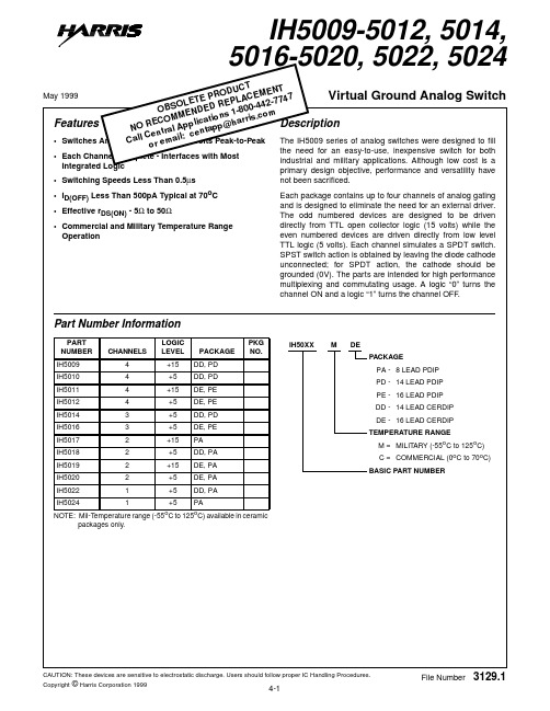
Features •Switches Analog Signals Up to 20 Volts Peak-to-Peak •Each Channel Complete - Interfaces with MostIntegrated Logic •Switching Speeds Less Than 0.5µs •I D(OFF) Less Than 500pA Typical at 70o C •Effective r DS(ON) - 5Ω to 50Ω•Commercial and Military Temperature Range OperationDescription The IH5009series of analog switches were designed to fill the need for an easy-to-use,inexpensive switch for both industrial and military applications.Although low cost is a primary design objective,performance and versatility have not been sacrificed.Each package contains up to four channels of analog gating and is designed to eliminate the need for an external driver.The odd numbered devices are designed to be driven directly from TTL open collector logic (15volts)while the even numbered devices are driven directly from low level TTL logic (5volts).Each channel simulates a SPDT switch.SPST switch action is obtained by leaving the diode cathode unconnected;for SPDT action,the cathode should be grounded (0V).The parts are intended for high performance multiplexing and commutating usage.A logic “0”turns the channel ON and a logic “1” turns the channel OFF .Part Number InformationPART NUMBER CHANNELSLOGIC LEVEL PACKAGE PKG NO.IH50094+15DD, PD IH50104+5DD, PD IH50114+15DE, PE IH50124+5DE, PE IH50143+5DD, PD IH50163+5DE, PE IH50172+15PA IH50182+5DD, PA IH50192+15DE, PA IH50202+5DE, PA IH50221+5DD, PA IH50241+5PANOTE:Mil-Temperature range (-55o C to 125o C)available in ceramicpackages only.IH50XXMDEPACKAGEPA -8 LEAD PDIP PD -14 LEAD PDIP PE -16 LEAD PDIP DD -14 LEAD CERDIP DE -16 LEAD CERDIP TEMPERATURE RANGEM =MILITARY (-55o C to 125o C)C =COMMERCIAL (0o C to 70o C)BASIC PART NUMBERMay 1999CAUTION: These devices are sensitive to electrostatic discharge. Users should follow proper IC Handling Procedures.IH5009-5012, 5014,5016-5020, 5022, 5024Virtual Ground Analog Switch File Number3129.1O B S O L E T E P R O D U C T N O R E C O M M E N D E D RE P L A C E M E N T C a l l C e n t r a l A p p l i c a t i o n s1-800-442-7747o r e m a i l: c e n t a p p @h a r r i s .c o m元器件交易网Functional Diagrams (Numbers in brackets refer to CERDIP Packages)IH5009, IH5010(14 LEAD CERDIP, 14 LEAD PDIP)IH5011, IH5012(16 LEAD CERDIP, 16 LEAD PDIP)IH5014(14 LEAD CERDIP, 14 LEAD PDIP)IH5016(16 LEAD CERDIP, 16 LEAD PDIP)IH5017 (8 LEAD PDIP)IH5018 (8 LEAD PDIP, 14 LEAD CERDIP)IH5019, IH5020(8 LEAD PDIP, 16 LEAD CERDIP)IH5022(8 LEAD PDIP, 14 LEAD CERDIP)IH5024(8 LEAD PDIP)Absolute Maximum Ratings Thermal InformationPositive Analog Signal Voltage. . . . . . . . . . . . . . . . . . . . . . . . . .30V Negative Analog Signal Voltage. . . . . . . . . . . . . . . . . . . . . . . . .-15V Diode Current. . . . . . . . . . . . . . . . . . . . . . . . . . . . . . . . . . . . . .10mA Power Dissipation (Note) . . . . . . . . . . . . . . . . . . . . . . . . . . .500mW Operating ConditionsTemperature Range5009C Series . . . . . . . . . . . . . . . . . . . . . . . . . . . . . . .0o C to 70o C 5009M Series . . . . . . . . . . . . . . . . . . . . . . . . . . . .-55o C to 125o C Maximum Storage Temperature Range . . . . . . . . . .-65o C to 150o C Maximum Lead T emperature (Soldering 10s). . . . . . . . . . . . .300o CCAUTION:Stresses above those listed in“Absolute Maximum Ratings”may cause permanent damage to the device.This is a stress only rating and operation of the device at these or any other conditions above those indicated in the operational sections of this specification is not implied.NOTE:Dissipation rating assumes device is mounted with all leads welded or soldered to printed circuit board in ambient temperature below 75o C. For higher temperature, derate at rate of 5m/W o C.Electrical Specifications(Per Channel)PARAMETER (NOTE 1)SYMBOL(NOTE 4)TESTCONDITIONS(NOTE 2)TYPE-55o C (M)0o C (C)MIN/MAX25o C125o C(M)70o C (C)MIN/MAX UNITSTYP MIN/MAXInput Current-ON I IN(ON)ALL V IN = 0V, I D = 2mA-0.01±0.5100µA Input Current-OFF I IN(OFF)5V Logic Ckts V IN = +4.5V,V A =±10V-0.04±0.520nAInput Current-OFF I IN(OFF)15V Logic Ckts V IN = +11V,V A =±10V-0.04±0.520nAChannel ControlVoltage-ONV IN(ON)5V Logic Ckts Note 30.5-0.50.5VChannel ControlVoltage-ONV IN(ON)15V Logic Ckts Note 3 1.5- 1.5 1.5VChannel ControlVoltage-OFFV IN(OFF)5V Logic Ckts Note 3-- 4.5 4.5VChannel ControlVoltage-OFFV IN(OFF)15V Logic Ckts Note 3--11.011.0VLeakage Current-OFF I D(OFF)5V Logic Ckts V IN = +4.5V,V A =±10V-0.02±0.520nALeakage Current-OFF I D(OFF)15V Logic Ckts V IN = +11V,V A =±10V-0.02±0.520nALeakage Current-ON I D(ON)5V Logic Ckts V IN = 0V, I S = 1mA-0.30±1.01000 (M)200 (C)nALeakage Current-ON I D(ON)15V Logic Ckts V IN = 0V, I S = 1mA-0.10±0.5500 (M)100 (C)nA Leakage Current-ON I D(ON)5V Logic Ckts V IN = 0V, I S = 2mA-- 1.010µA Leakage Current-ON I D(ON)15V Logic Ckts V IN = 0V, I S = 2mA-- 2.0100µADrain-Source ON-Resistance r DS(ON)5V Logic Ckts I D = 2mA, V IN = 0.5V150******** (M)240 (C)ΩDrain-Source ON-Resistance r DS(ON)15V Logic Ckts I D = 2mA, V IN = 1.5V10080100250 (M)160 (C)ΩTurn-ON Time t(ON)All-150500-ns Turn-OFF Time t(OFF)All-300500-ns Cross Talk CT All f = 100Hz-120--dB NOTES:1.(OFF) and (ON) subscript notation refers to the conduction state of the FET switch for the given test.2.Refer to Figure 1 for definition of terms.3.V IN(ON) and V IN(OFF) are test conditions guaranteed by the tests of r DS(ON)and I D(OFF) respectively.4.“5V Logic CKTS” applies to even-numbered devices. “15V Logic CKTS” applies to odd-numbered devices.。

SM5010 seriesCrystal Oscillator Module ICs OVERVIEWThe SM5010 series are crystal oscillator module ICs. They incorporate oscillator and output buffer circuits, employing built-in oscillator capacitors and feedback resistors with excellent frequency response, eliminating the need for external components to form a stable crystal oscillator. There are 7 oscillator configurations available for design and application optimization.FEATURESI7 types of oscillation circuit structureFor fundamental oscillator•5010A××:Simple structure with low frequency vari-ation•5010B××:Low crystal current type with R D built-inoscillation circuit•5010CL×:Oscillation stop function built-in •5010DN×:External capacitors, C G and C D required •5010EA×:Low current consumption typeFor 3rd overtone oscillator•5010F××:Suitable for round blank•5010H××:External resistor, R f required I 2.7 to 5.5V operating supply voltageI Capacitors C G, C D built-inI Inverter amplifier feedback resistor built-inI Output duty level•TTL level: AK×, BK×, HKוCMOS level:AN×, AH×, BN×, BH×, CL×, DN×,EA×, FN×, FH×, HN×I Oscillator frequency output (f O, f O/2, f O/4, f O/8, f O/16determined by internal connection)I Standby functionI Pull-up resistor built-inI8-pin SOP (SM5010×××S)I Chip form (CF5010×××)SERIES CONFIGURATION For Fundamental OscillatorVersion1Operatingsupplyvoltage range[V]Built-incapacitance RD[Ω]Outputcurrent(V DD = 5V)[mA]Output dutylevelOutputfrequencyINHN inputlevel(V DD = 5V)Standby modeC G[pF]C D[pF]Oscillatorstop function Output stateCF5010AN12.7 to 5.52929–16CMOS f OTTL No High impedanceCF5010AN2CMOS/TTL f O/2CF5010AN3f O/4CF5010AN4f O/8CF5010AK1 4.5 to 5.52929–16TTL f O TTL No High impedanceCF5010AH12.7 to 5.52929–4CMOS f OTTL No High impedanceCF5010AH2f O/2 CF5010AH3f O/4 CF5010AH4f O/8CF5010BN12.7 to 5.5222282016CMOS f OTTL No High impedanceCF5010BN2CMOS/TTL f O/2CF5010BN3f O/4CF5010BN4f O/8CF5010BN5f O/16CF5010BK1 4.5 to 5.5222282016TTL f O TTL No High impedanceCF5010BH12.7 to 5.522228204CMOS f OTTL No High impedanceCF5010BH2f O/2 CF5010BH3f O/4 CF5010BH4f O/8CF5010CL12.7 to 5.51818–16CMOS f OCMOS Yes High impedanceCF5010CL2f O/2CF5010CL3f O/4CF5010CL4f O/8CF5010CL5f O/16CF5010DN1 2.7 to 5.5––82016CMOS f O TTL No High impedanceCF5010EA12.7 to 5.510158204CMOS f OTTL Yes LOWCF5010EA2f O/21. Package devices have designation SM5010×××S.元器件交易网SM5010 seriesSERIES CONFIGURATIONFor 3rd Overtone OscillatorORDERING INFORMATIONPACKAGE DIMENSIONS(Unit: mm) • 8-pin SOPVersion Operating supply voltage range [V]gm ratioBuilt-in capacitanceR f [k Ω ]Output current (V DD = 5V) [mA]Output duty levelC G [pF]CD [pF] CF5010FNA 2.7 to 5.51.001315 4.216CMOSCF5010FNC 1117 3.1CF5010FND 1317 2.2CF5010FNE 4.5 to 5.5815 2.2CF5010FHA 4.5 to 5.51.001315 4.24CMOSCF5010FHC 1117 3.1CF5010FHD 1317 2.2CF5010FHE 815 2.2CF5010HN1 4.5 to 5.5 1.17131720016CMOS CF5010HK14.5 to5.51.17131720016TTLDevice Package SM5010 ××× S 8-pin SOP CF5010 ×××–1Chip form元器件交易网SM5010 seriesPAD LAYOUT(Unit: µ m)PINOUT(Top view)PIN DESCRIPTION and PAD DIMENSIONSNumberNameI/ODescriptionPad dimensions [µm]X Y 1INHN I Output state control input. Standby mode when LOW, pull-up resistor built in. In the case of the 5010CL × , the oscillator stops and Power-saving pull-up resistor is built-in to reduce current consumption at standby mode.195174.42XT I Amplifier input.Crystal oscillator connection pins.Crystal oscillator connected between XT and XTN385174.43XTN O Amplifier output.575174.44VSS –Ground765174.45Q O Output. Output frequency (f O , f O /2, f O /4, f O /8, f O/16) determined by internal connection 757.61017.66NC –No connection ––7NC –No connection ––8VDD–Supply voltage165.41014.6元器件交易网元器件交易网SM5010 series BLOCK DIAGRAMFor Fundamental OscillatorI5010A××, B××, CL×, DN×, EA× seriesFor 3rd Overtone OscillatorI5010F××, H×× seriesSM5010 seriesFUNCTIONAL DESCRIPTIONStandby Function5010AH × , AK × , AN × , BH × , BK × , BN × , DN×, FN ×, FH ×, HN ×, HK × seriesWhen INHN goes LOW, the output on Q becomes high impedance, but internally the oscillator does not stop.5010CL × seriesWhen INHN goes LOW, the oscillator stops and the oscillator output on Q becomes high impedance.5010EA × seriesWhen INHN goes LOW, the oscillator stops and the oscillator output on Q becomes LOW.Power-saving Pull-up Resistor (CL series only)The INHN pull-up resistance changes in response to the input level (HIGH or LOW). When INHN goes LOW (standby state), the pull-up resistance becomes large to reduce the current consumption during standby.Version INHN QOscillator AH ×, AK ×, AN ×, BH ×, BK ×, BN ×, DN ×, FH ×, FH ×, HN ×, HK × seriesHIGH (or open)Any f O , f O /2, f O /4, f O /8 or f O /16 output frequencyNormal operation LOW High impedanceNormal operation CL × seriesHIGH (or open)Any f O , f O /2, f O /4, f O /8 or f O /16 output frequencyNormal operationLOW High impedanceStopped EA × seriesHIGH (or open)Either f O or f O /2 output frequencyNormal operationLOWLOWStopped元器件交易网SPECIFICATIONSAbsolute Maximum RatingsV SS = 0VRecommended Operating Conditions3V operation V SS = 0VParameterSymbol ConditionRating Unit Supply voltage range V DD −0.5 to +7.0V Input voltage range V IN −0.5 to V DD + 0.5V Output voltage range V OUT −0.5 to V DD + 0.5V Operating temperature range T opr −40 to +85°C Storage temperature rangeT stgChip form −65 to +150°C8-pin SOP−55 to +125Output currentI OUT AH ×, BH ×, FH ×, EA ×10mA AN ×, AK ×, BN ×, BK ×, CL ×, DN ×, FN ×, HN ×, HK ×25Power dissipation P D8-pin SOP500mWParameter Symbol Version ConditionRating Unit Operating supply voltage V DD All version 2.7 to 3.6V Input voltageV INAll version V SS to V DDVOperating temperatureT OPR5010AN ×−10 to +70°C5010AH ×5010BN ×5010BH ×5010CL ×−20 to +805010DN1−10 to +705010EA ×5010FN ×Operating frequencyf5010AN ×C L ≤ 15pF2 to 30MHz5010AH × 2 to 165010BN ×2 to 305010BH × 2 to 165010CL × 2 to 305010DN15010EA ×5010FN ×22 to 405V operationV SS = 0VParameter Symbol Version Condition Rating Unit Operating supply voltage V DD All version 4.5 to 5.5V Input voltage V IN All version V SS to V DD VOperating temperature T OPR 5010AN×−40 to +85°C 5010AK×5010AH×5010BN×5010BK×5010BH×5010CL×5010DN15010EA×C L≤ 15pF, f = 2 to 30MHzC L≤ 15pF, f = 2 to 40MHz−10 to +705010FN×C L≤ 50pF, 30MHz ≤ f ≤ 50MHz−20 to +80C L≤ 15pF, 50MHz ≤ f ≤ 70MHz−15 to +755010FH×C L≤ 15pF, 30MHz ≤ f ≤ 50MHz−20 to +80C L≤ 15pF, 50MHz ≤ f ≤ 60MHz−15 to +755010HN1−40 to +855010HK1Operating frequency f 5010AN×C L≤ 50pF2 to 30MHz 5010AK×C L≤ 15pF5010AH×5010BN×C L≤ 50pF5010BK×C L≤ 15pF5010BH×5010CL×C L≤ 50pF5010DN15010EA×C L≤ 15pF, Ta =− 40 to + 85°C 2 to 405010FN×C L≤ 50pF, Ta =− 20 to + 80°C30 to 50C L≤ 15pF, Ta =− 15 to + 75°C50 to 705010FH×C L≤ 15pF, Ta =− 20 to + 80°C30 to 50C L≤ 15pF, Ta =− 15 to + 75°C50 to 605010HN1C L≤ 50pF22 to 505010HK1C L≤ 15pFElectrical Characteristics5010AN ×, BN ×, DN × series3V operation: V DD = 2.7 to 3.6V , V SS = 0V , Ta = −10 to +70°C unless otherwise noted.5010AN ×, AK ×, BN ×, BK ×, DN × series5V operation: V DD = 4.5 to 5.5V , V SS = 0V , Ta = −40 to +85°C unless otherwise noted.Parameter Symbol ConditionRatingUnit min typ max HIGH-level output voltage V OH Q: Measurement cct 1, V DD = 2.7V, I OH = 8mA 2.1 2.4–V LOW-level output voltage V OL Q: Measurement cct 2, V DD = 2.7V, I OL = 8mA –0.30.4V HIGH-level input voltage V IH INHN 2.0––V LOW-level input voltage V IL INHN––0.5V Output leakage currentI ZQ: Measurement cct 2, INHN = LOW, V DD = 3.6VV OH = V DD ––10µAV OL = V SS ––10Current consumptionI DDMeasurement cct 3, load cct 1,INHN = open, C L = 15pF , f = 30MHz5010×N1–510mA 5010×N2– 3.575010×N3– 2.555010×N4–245010×N5–24INHN pull-up resistance R UP2Measurement cct 440100250k ΩFeedback resistance R f Measurement cct 580200500k ΩOscillator amplifier output resistanceR D Design value5010B ××690820940ΩBuilt-in capacitanceC GDesign value. A monitor pattern on a wafer is tested.5010A ××262932pF 5010B ××202224C D5010A ××2629325010B ××202224Parameter Symbol ConditionRatingUnit min typ max HIGH-level output voltage V OH Q: Measurement cct 1, V DD = 4.5V, I OH = 16mA 3.9 4.2–V LOW-level output voltage V OL Q: Measurement cct 2, V DD = 4.5V, I OL = 16mA –0.30.4V HIGH-level input voltage V IH INHN 2.0––V LOW-level input voltage V IL INHN––0.8V Output leakage currentI ZQ: Measurement cct 2, INHN = LOW, V DD = 5.5VV OH = V DD ––10µAV OL = V SS ––10Current consumptionI DDMeasurement cct 3, load cct 1, INHN = open, C L = 50pF , f = 30MHz5010×N1–1530mA 5010×N2–9185010×N3–6125010×N4–5105010×N5–510Measurement cct 3, load cct 2,INHN = open, C L = 15pF , f = 30MHz5010×K1–1020INHN pull-up resistance R UP2Measurement cct 440100250k ΩFeedback resistance R f Measurement cct 580200500k ΩOscillator amplifier output resistanceR D Design value5010B ××690820940ΩBuilt-in capacitanceC GDesign value. A monitor pattern on a wafer is tested.5010A ××262932pF 5010B ××202224C D5010A ××2629325010B ××2022245010AH ×, BH × series3V operation: V DD = 2.7 to 3.6V , V SS = 0V , Ta = −10 to +70°C unless otherwise noted.5V operation: V DD = 4.5 to 5.5V , V SS = 0V , Ta = −40 to +85°C unless otherwise noted.Parameter Symbol ConditionRatingUnit min typ max HIGH-level output voltage V OH Q: Measurement cct 1, V DD = 2.7V, I OH = 2mA 2.1 2.4–V LOW-level output voltage V OL Q: Measurement cct 2, V DD = 2.7V, I OL = 2mA –0.30.5V HIGH-level input voltage V IH INHN 2.0––V LOW-level input voltage V IL INHN––0.5V Output leakage currentI ZQ: Measurement cct 2, INHN = LOW, V DD = 3.6VV OH = V DD ––10µAV OL = V SS ––10Current consumptionI DDMeasurement cct 3, load cct 1,INHN = open, C L = 15pF , f = 16MHz5010×H1–36mA 5010×H2–245010×H3– 1.535010×H4– 1.5 2.5INHN pull-up resistance R UP2Measurement cct 440100250k ΩFeedback resistance R f Measurement cct 580200500k ΩOscillator amplifier output resistanceR D Design value5010B ××690820940ΩBuilt-in capacitanceC GDesign value. A monitor pattern on a wafer is tested.5010A ××262932pF 5010B ××202224C D5010A ××2629325010B ××202224Parameter Symbol ConditionRatingUnit min typ max HIGH-level output voltage V OH Q: Measurement cct 1, V DD = 4.5V, I OH = 4mA 3.9 4.2–V LOW-level output voltage V OL Q: Measurement cct 2, V DD = 4.5V, I OL = 4mA –0.30.5V HIGH-level input voltage V IH INHN 2.0––V LOW-level input voltage V IL INHN––0.8V Output leakage currentI ZQ: Measurement cct 2, INHN = LOW, V DD = 5.5VV OH = V DD ––10µAV OL = V SS ––10Current consumptionI DDMeasurement cct 3, load cct 1,INHN = open, C L = 15pF , f = 30MHz5010×H1–918mA 5010×H2–6125010×H3–5105010×H4–48INHN pull-up resistance R UP2Measurement cct 440100250k ΩFeedback resistance R f Measurement cct 580200500k ΩOscillator amplifier output resistanceR D Design value5010B ××690820940ΩBuilt-in capacitanceC GDesign value. A monitor pattern on a wafer is tested.5010A ××262932pF 5010B ××202224C D5010A ××2629325010B ××2022245010CL × series3V operation: V DD = 2.7 to 3.6V , V SS = 0V , Ta = −20 to +80°C unless otherwise noted.5V operation: V DD = 4.5 to 5.5V , V SS = 0V , Ta = −40 to +85°C unless otherwise noted.Parameter Symbol ConditionRatingUnit min typ max HIGH-level output voltage V OH Q: Measurement cct 1, V DD = 2.7V, I OH = 8mA 2.2 2.4–V LOW-level output voltage V OL Q: Measurement cct 2, V DD = 2.7V, I OL = 8mA –0.30.4V HIGH-level input voltage V IH INHN 0.7V DD ––V LOW-level input voltage V IL INHN––0.3V DD V Output leakage currentI ZQ: Measurement cct 2, INHN = LOW, V DD = 3.6VV OH = V DD ––10µAV OL = V SS ––10Current consumptionI DDMeasurement cct 3, load cct 1,INHN = open, C L = 15pF , f = 30MHz5010CL1–510mA 5010CL2– 3.575010CL3– 2.555010CL4–245010CL5–24Standby current I ST Measurement cct 6, INHN = LOW ––5µA INHN pull-up resistance R UP1Measurement cct 42415M ΩR UP240100250k ΩFeedback resistance R f Measurement cct 580200500k ΩBuilt-in capacitanceC G Design value. A monitor pattern on a wafer is tested.161820pF C D161820Parameter Symbol ConditionRatingUnit min typ max HIGH-level output voltage V OH Q: Measurement cct 1, V DD = 4.5V, I OH = 16mA 4.0 4.2–V LOW-level output voltage V OL Q: Measurement cct 2, V DD = 4.5V, I OL = 16mA –0.30.4V HIGH-level input voltage V IH INHN 0.7V DD ––V LOW-level input voltage V IL INHN––0.3V DD V Output leakage currentI ZQ: Measurement cct 2, INHN = LOW, V DD = 5.5VV OH = V DD ––10µAV OL = V SS ––10Current consumptionI DDMeasurement cct 3, load cct 1,INHN = open, C L = 50pF , f = 30MHz5010CL1–1530mA 5010CL2–9185010CL3–6125010CL4–5105010CL5–510Standby current I ST Measurement cct 6, INHN = LOW ––10µA INHN pull-up resistance R UP1Measurement cct 4128M ΩR UP240100250k ΩFeedback resistance R f Measurement cct 580200500k ΩBuilt-in capacitanceC G Design value. A monitor pattern on a wafer is tested.161820pF C D1618205010EA × series3V operation: V DD = 2.7 to 3.6V , V SS = 0V , Ta = −10 to +70°C unless otherwise noted.5V operation: V DD = 4.5 to 5.5V , V SS = 0V , Ta = −40 to +85°C unless otherwise noted.Parameter Symbol ConditionRatingUnit min typ max HIGH-level output voltage V OH Q: Measurement cct 1, V DD = 2.7V, I OH = 2mA 2.1 2.4–V LOW-level output voltage V OL Q: Measurement cct 2, V DD = 2.7V, I OL = 2mA –0.30.5V HIGH-level input voltage V IH INHN 2.0––V LOW-level input voltage V IL INHN––0.5V Current consumption I DD Measurement cct 3, load cct 1,INHN = open, C L = 15pF , f = 30MHz 5010EA1–48mA 5010EA2– 2.55INHN pull-up resistance R UP2Measurement cct 440100250k ΩFeedback resistance R f Measurement cct 580200500k ΩOscillator amplifier output resistance R D Design value690820940ΩBuilt-in capacitanceC G Design value. A monitor pattern on a wafer is tested.91011pFC D131517Parameter Symbol ConditionRatingUnit min typ max HIGH-level output voltage V OH Q: Measurement cct 1, V DD = 4.5V, I OH = 3.2mA 3.9 4.2–V LOW-level output voltage V OL Q: Measurement cct 2, V DD = 4.5V, I OL = 3.2mA –0.30.4V HIGH-level input voltage V IH INHN 2.0––V LOW-level input voltageV IL INHN––0.8VCurrent consumptionI DD1Measurement cct 3, load cct 1,INHN = open, C L = 15pF , f = 30MHz5010EA1–612mA 5010EA2–510I DD2Measurement cct 3, load cct 1,INHN = open, C L = 15pF , f = 40MHz 5010EA1–9185010EA2–612INHN pull-up resistance R UP2Measurement cct 440100250k ΩFeedback resistance R f Measurement cct 580200500k ΩOscillator amplifier output resistance R D Design value690820940ΩBuilt-in capacitanceC G Design value. A monitor pattern on a wafer is tested.91011pFC D1315175010FN× series3V operation: V DD = 2.7 to 3.6V, V SS = 0V, Ta = −10 to +70°C unless otherwise noted.Parameter Symbol ConditionRatingUnit min typ maxHIGH-level output voltage V OH Q: Measurement cct 1, V DD = 2.7V, I OH = 8mA 2.2 2.4–V LOW-level output voltage V OL Q: Measurement cct 2, V DD = 2.7V, I OL = 8mA–0.30.4V HIGH-level input voltage V IH INHN 2.0––V LOW-level input voltage V IL INHN––0.5VOutput leakage current I Z Q: Measurement cct 2, INHN = LOW,V DD = 3.6VV OH = V DD––10µAV OL = V SS––10Current consumption I DD Measurement cct 3, load cct 1,INHN = open, C L = 15pF5010FNA, FNCf = 30MHz–816mA5010FNDf = 40MHz–1020INHN pull-up resistance R UP Measurement cct 440100250kΩFeedback resistance R f Measurement cct 55010FNA 3.57 4.2 4.83kΩ5010FNC 2.63 3.1 3.575010FND 1.87 2.2 2.53Built-in capacitance C GDesign value. A monitor pattern on awafer is tested.5010FNA11.71314.3pF5010FNC9.91112.15010FND11.71314.3C D5010FNA13.51516.55010FNC15.31718.75010FND15.31718.75V operation:V DD = 4.5 to 5.5V, V SS = 0V30 ≤ f ≤ 50MHz: Ta = −20 to +80°C, 50 < f ≤ 70MHz: Ta = −15 to +75°C unless otherwise noted.Parameter Symbol ConditionRatingUnit min typ maxHIGH-level output voltage V OH Q: Measurement cct 1, V DD = 4.5V, I OH = 16mA 3.9 4.2–V LOW-level output voltage V OL Q: Measurement cct 2, V DD = 4.5V, I OL = 16mA–0.30.4V HIGH-level input voltage V IH INHN 2.0––V LOW-level input voltage V IL INHN––0.8VOutput leakage current I Z Q: Measurement cct 2, INHN = LOW,V DD = 5.5VV OH = V DD––10µAV OL = V SS––10Current consumption I DD1Measurement cct 3, load cct 1,INHN = open, C L = 15pF5010FNEf = 70MHz–2550mA I DD2Measurement cct 3, load cct 1,INHN = open, C L = 50pF5010FNA, FNCf = 40MHz–23455010FNDf = 50MHz–2550INHN pull-up resistance R UP Measurement cct 440100250kΩFeedback resistance R f Measurement cct 55010FNA 3.57 4.2 4.83kΩ5010FNC 2.63 3.1 3.575010FND 1.87 2.2 2.535010FNE 1.87 2.2 2.53Built-in capacitance C GDesign value. A monitor pattern on awafer is tested.5010FNA11.71314.3pF5010FNC9.91112.15010FND11.71314.35010FNE7.288.8C D5010FNA13.51516.55010FNC15.31718.75010FND15.31718.75010FNE13.51516.55010FH × series5V operation:V DD = 4.5 to 5.5V , V SS = 0V30 ≤ f ≤ 50MHz: Ta = −20 to +80°C, 50 < f ≤ 60MHz: Ta = −15 to +75°C unless otherwise noted.5010HN ×, HK × series5V operation: V DD = 4.5 to 5.5V , V SS = 0V , Ta = −40 to +85°C unless otherwise noted.Parameter Symbol ConditionRatingUnit min typ max HIGH-level output voltage V OH Q: Measurement cct 1, V DD = 4.5V, I OH = 4mA 3.9 4.2–V LOW-level output voltage V OL Q: Measurement cct 2, V DD = 4.5V, I OL = 4mA –0.30.5V HIGH-level input voltage V IH INHN 2.0––V LOW-level input voltage V IL INHN––0.8V Output leakage currentI ZQ: Measurement cct 2, INHN = LOW, V DD = 5.5VV OH = V DD ––10µAV OL = V SS ––10Current consumptionI DDMeasurement cct 3, load cct 1,INHN = open, C L = 15pF5010FHA, FHC f = 40MHz–1326mA 5010FHD f = 50MHz –15305010FHE f = 60MHz–1734INHN pull-up resistanceR UPMeasurement cct 440100250k ΩFeedback resistanceR fMeasurement cct 55010FHA3.574.2 4.83k Ω5010FHC 2.63 3.1 3.575010FHD 1.87 2.2 2.535010FHE 1.87 2.2 2.53Built-in capacitanceC GDesign value. A monitor pattern on a wafer is tested.5010FHA11.71314.3pF 5010FHC 9.91112.15010FHD 11.71314.35010FHE 7.288.8C D5010FHA 13.51516.55010FHC 15.31718.75010FHD 15.31718.75010FHE13.51516.5Parameter Symbol ConditionRatingUnit min typ max HIGH-level output voltage V OH Q: Measurement cct 1, V DD = 4.5V, I OH = 16mA 3.9 4.2–V LOW-level output voltage V OL Q: Measurement cct 2, V DD = 4.5V, I OL = 16mA –0.30.4V HIGH-level input voltage V IH INHN 2.0––V LOW-level input voltage V IL INHN––0.8V Output leakage currentI Z Q: Measurement cct 2, INHN = LOW, V DD = 5.5VV OH = V DD ––10µAV OL = V SS ––10Current consumptionI DD1Measurement cct 3, load cct 2,INHN = open, C L = 15pF , f = 50MHz 5010HK1–2040mAI DD2Measurement cct 3, load cct 1,INHN = open, C L = 50pF , f = 50MHz 5010HN1–2550INHN pull-up resistance R UP Measurement cct 440100250k ΩFeedback resistance R f Measurement cct 580200500k ΩBuilt-in capacitanceC G Design value. A monitor pattern on a wafer is tested.11.71314.3pF C D15.31718.7Switching Characteristics5010AN ×, BN ×, DN × series3V operation/Duty level: CMOSV DD = 2.7 to 3.6V , V SS = 0V , Ta = −10 to +70°C unless otherwise noted.5010AN ×, AK ×, BN ×, BK ×, DN × series5V operation/Duty level: CMOS (5010AN ×, BN ×, DN1)V DD = 4.5 to 5.5V , V SS = 0V , Ta = −40 to +85°C unless otherwise noted.5V operation/Duty level: TTL (5010×K1, AN2, AN3, AN4, BN2, BN3, BN4, BN5)V DD = 4.5 to 5.5V , V SS = 0V , Ta = −40 to +85°C unless otherwise noted.Parameter Symbol ConditionRatingUnit min typ max Output rise time t r1Measurement cct 6, load cct 1, C L = 15pF , 0.1V DD to 0.9V DD – 3.0 6.0ns Output fall time t f1Measurement cct 6, load cct 1, C L = 15pF , 0.9V DD to 0.1V DD – 3.0 6.0ns Output duty cycle 11. The duty cycle characteristic is checked the sample chips of each production lot.Duty Measurement cct 6, load cct 1, V DD = 3.0V, Ta = 25°C, C L = 15pF , f = 30MHz40–60%Output disable delay time t PLZ Measurement cct 7, load cct 1, V DD = 3.0V, Ta = 25°C, C L = 15pF––100ns Output enable delay timet PZL––100nsParameterSymbol ConditionRatingUnitmin typ max Output rise time t r1Measurement cct 6, load cct 1, 0.1V DD to 0.9V DDC L = 15pF – 2.0 4.0nst r2C L = 50pF – 4.08.0Output fall time t f1Measurement cct 6, load cct 1, 0.9V DD to 0.1V DDC L = 15pF – 2.0 4.0nst f2C L = 50pF– 4.08.0Output duty cycle 11. The duty cycle characteristic is checked the sample chips of each production lot.Duty Measurement cct 6, load cct 1, V DD = 5.0V, Ta = 25°C, C L = 50pF , f = 30MHz45–55%Output disable delay time t PLZ Measurement cct 7, load cct 1, V DD = 5.0V, Ta = 25°C, C L = 15pF––100ns Output enable delay timet PZL––100nsParameter Symbol ConditionRatingUnit min typ max Output rise time t r3Measurement cct 6, load cct 2, C L = 15pF , 0.4V to 2.4V – 1.5 3.0ns Output fall time t f3Measurement cct 6, load cct 2, C L = 15pF , 2.4V to 0.4V – 1.5 3.0ns Output duty cycle 11. The duty cycle characteristic is checked the sample chips of each production lot.Duty Measurement cct 6, load cct 2, V DD = 5.0V, Ta = 25°C, C L = 15pF , f = 30MHz45–55%Output disable delay time t PLZ Measurement cct 7, load cct 2, V DD = 5.0V, Ta = 25°C, C L = 15pF––100ns Output enable delay timet PZL––100ns5010AH ×, BH × series3V operation/Duty level: CMOSV DD = 2.7 to 3.6V , V SS = 0V , Ta = −10 to +70°C unless otherwise noted.5V operation/Duty level: CMOSV DD = 4.5 to 5.5V , V SS = 0V , Ta = −40 to +85°C unless otherwise noted.Parameter Symbol ConditionRatingUnit min typ max Output rise time t r1Measurement cct 6, load cct 1, C L = 15pF , 0.1V DD to 0.9V DD –816ns Output fall time t f1Measurement cct 6, load cct 1, C L = 15pF , 0.9V DD to 0.1V DD –816ns Output duty cycle 11. The duty cycle characteristic is checked the sample chips of each production lot.Duty Measurement cct 6, load cct 1, V DD = 3.0V, Ta = 25°C, C L = 15pF , f = 16MHz40–60%Output disable delay time t PLZ Measurement cct 7, load cct 1, V DD = 3.0V, Ta = 25°C, C L = 15pF––100ns Output enable delay timet PZL––100nsParameterSymbol ConditionRatingUnitmin typ max Output rise time t r1Measurement cct 6, load cct 1, 0.1V DD to 0.9V DDC L = 15pF –510nst r2C L = 50pF –1326Output fall time t f1Measurement cct 6, load cct 1, 0.9V DD to 0.1V DDC L = 15pF –510nst f2C L = 50pF–1326Output duty cycle 11. The duty cycle characteristic is checked the sample chips of each production lot.Duty Measurement cct 6, load cct 1, V DD = 5.0V, Ta = 25°C, C L = 15pF , f = 30MHz45–55%Output disable delay time t PLZ Measurement cct 7, load cct 1, V DD = 5.0V, Ta = 25°C, C L = 15pF––100ns Output enable delay timet PZL––100ns5010CL × series3V operation/Duty level: CMOSV DD = 2.7 to 3.6V , V SS = 0V , Ta = −20 to +80°C unless otherwise noted.5V operation/Duty level: CMOSV DD = 4.5 to 5.5V , V SS = 0V , Ta = −40 to +85°C unless otherwise noted.ParameterSymbol ConditionRatingUnitmin typ max Output rise time t r1Measurement cct 6, load cct 1, 0.1V DD to 0.9V DDC L = 15pF – 2.0 4.0nst r4C L = 30pF – 3.0 6.0Output fall time t f1Measurement cct 6, load cct 1, 0.9V DD to 0.1V DDC L = 15pF – 2.0 4.0nst f4C L = 30pF– 3.0 6.0Output duty cycle 11. The duty cycle characteristic is checked the sample chips of each production lot.Duty Measurement cct 6, load cct 1, V DD = 3.0V, Ta = 25°C, C L = 15pF , f = 30MHz45–55%Output disable delay time 22. Oscillator stop function is built-in. When INHN goes LOW, normal output stops. When INHN goes HIGH, normal output is not resumed until after the oscillator start-up time has elapsed.t PLZ Measurement cct 7, load cct 1, V DD = 3.0V, Ta = 25°C, C L = 15pF––100ns Output enable delay time 2t PZL––100nsParameterSymbol ConditionRatingUnitmin typ max Output rise time t r1Measurement cct 6, load cct 1, 0.1V DD to 0.9V DDC L = 15pF – 1.5 3.0nst r2C L = 50pF – 4.08.0Output fall time t f1Measurement cct 6, load cct 1, 0.9V DD to 0.1V DDC L = 15pF – 1.5 3.0nst f2C L = 50pF– 4.08.0Output duty cycle 11. The duty cycle characteristic is checked the sample chips of each production lot.Duty Measurement cct 6, load cct 1, V DD = 5.0V, Ta = 25°C, C L = 50pF , f = 30MHz40–60%Output disable delay time 22. Oscillator stop function is built-in. When INHN goes LOW, normal output stops. When INHN goes HIGH, normal output is not resumed until after the oscillator start-up time has elapsed.t PLZ Measurement cct 7, load cct 1, V DD = 5.0V, Ta = 25°C, C L = 15pF––100ns Output enable delay time 2t PZL––100ns5010EA × series3V operation/Duty level: CMOSV DD = 2.7 to 3.6V , V SS = 0V , Ta = −10 to +70°C unless otherwise noted.5V operation/Duty level: CMOSV DD = 4.5 to 5.5V , V SS = 0V , Ta = −40 to +85°C unless otherwise noted.Parameter Symbol ConditionRatingUnit min typ max Output rise time t r1Measurement cct 6, load cct 1, C L = 15pF , 0.1V DD to 0.9V DD –816ns Output fall time t f1Measurement cct 6, load cct 1, C L = 15pF , 0.9V DD to 0.1V DD –816ns Output duty cycle 11. The duty cycle characteristic is checked the sample chips of each production lot.Duty Measurement cct 6, load cct 1, V DD = 3.0V, Ta = 25°C, C L = 15pF , f = 30MHz40–60%Output disable delay time 22. Oscillator stop function is built-in. When INHN goes LOW, normal output stops. When INHN goes HIGH, normal output is not resumed until after the oscillator start-up time has elapsed.t PLZ Measurement cct 7, load cct 1, V DD = 3.0V, Ta = 25°C, C L = 15pF––100ns Output enable delay time 2t PZL––100nsParameterSymbol ConditionRatingUnitmin typ max Output rise time t r1Measurement cct 6, load cct 1, 0.1V DD to 0.9V DDC L = 15pF –510nst r2C L = 50pF –1326Output fall time t f1Measurement cct 6, load cct 1, 0.9V DD to 0.1V DDC L = 15pF –510nst f2C L = 50pF –1326Output duty cycle 11. The duty cycle characteristic is checked the sample chips of each production lot.Duty1Measurement cct 6, load cct 1, V DD = 5.0V, Ta = 25°C, C L = 15pFf = 30MHz 45–55%Duty2 f = 40MHz40–60Output disable delay time 22. Oscillator stop function is built-in. When INHN goes LOW, normal output stops. When INHN goes HIGH, normal output is not resumed until after the oscillator start-up time has elapsed.t PLZ Measurement cct 7, load cct 1, V DD = 5.0V, Ta = 25°C, C L = 15pF––100ns Output enable delay time 2t PZL––100ns。
过放试验
移除保护板,在20℃±5℃条件下,蓄电池以0.5C(A)
电流放电至电压达到0V。
电池组不漏液、不爆炸、
不起火
4.产品特征曲线图
4.1 15F50放电电压-容量特征曲线图
4.2 15F50先恒流后恒压(0.25C)充电曲线图 4.3 15F50循环寿命特征曲线图
5. 产品结构特性
整组产品外观图片
6. 贮存、维护与运输
6.1贮存
电池组需长期贮存时,请将电池组充电至50%左右的电量(放完电后,用10A恒流充电2小时即可),放置于干燥、通风处,每三个月循环一次。
电池组应贮存在清洁、干燥、通风处,应避免与腐蚀性物质接触,远离火源及热源。