第二讲-PSpice中的器件模型和模型参数
- 格式:pdf
- 大小:767.34 KB
- 文档页数:61


pspice二级管参数总结查看文章OrCAD PSpice DIODE model parameter 2010-07-15 22:311.从OrCAD PSpice help文档:2.国外网站的相关介绍:SPICE Diode Model Parametersname parameter units default example ar1 IS saturation current A 1.0e-14 1.0e-14 *2 RS ohmic resistanc Ohm 0 10 *3 N emission coefficient - 1 1.04 TT transit-time sec 0 0.1nsThe DC characteristics of the diode are determined by the parameters IS, N, and the ohmic resistance RS. Charge storage effects are modeled by a transit time, TT, and a nonlinear depletion layer capacitance whic determined by the parameters CJO, VJ, and M. The temperature dependence of the saturation current is defined by the parameters EG, the band gap energy and XTI, the saturation current temperature exponent. nominal temperature at which these parameters were measured is TNOM, which defaults to the circuit-wi value specified on the .OPTIONS control line. Reverse breakdown is modeled by an exponential increase the reverse diode current and is determined by the parameters BV and IBV (both of which are positive numbers).3. 国外网站关于PSpice 其它模型的参数介绍:如(三极管,达林顿管,场效应管,二极管)Spice modelsIntroductionThe MOD model fileThe ZMODELS.LIB library fileModel parameters and limitationso Bipolarso Darlingtonso MOSFETso DiodesFurther informationIntroductionZetex have created Spice models for a range of semiconductor components. Models included are Schottky varicap, high-performance bipolar (high current, low VCE(sat)), higher voltage bipolar, bipolar Darlingto and MOSFET transistors. This range is continuously under review as new products are introduced and retrospective models are generated for existing products.The Spice models are available in two formats:1. A separate Spice model text file for each Zetex device type for which a model is presently availabThese can be accessed from the Product Quickfinder2.All the available Zetex device models are collected together into a single .LIB text file calledZMODELS.LIB.A generic symbol library file is available called ZETEXM.SLB that enables Windows? versions of PSpic use the Zetex spice models. Further information on the symbol library, including installation instructions be found in the text file called ZETEXM.TXTThe MOD Model FileEach of these files is a Spice model for a single device. Theycan be loaded into your simulation simply b employing the Spice command <.include device_name.mod>. Only the device types specifically required the circuit under simulation need be included in this way. All diode and bipolar transistor models are simp <.model> files. However, Darlington transistors and MOSFET models are multi-component subcircuits an such are supplied as <.subckt> files.The diode models should be included in circuit files using the normal Spice reference .Bipolar transistor models should be included using .All other models should be referenced as subcircuits i.e. in the form for Darlington transistors, and for MOSFETs.The ZMODELS.LIB Library FileUsers may prefer to use the model library. This library is a collection of all Zetex Spice models exactly as t appear in the individual model files. By using the statement <.lib zmodels.lib>, Spice will be able to acce any model within the library without the need for multiple <.include> statements.Note:All subcircuits, whether in the library or as individual model files use the same connection sequence as Sp for single element models, thus easing their use.Model parameters and limitationsBipolarsDarlingtonsMOSFETsDiodesBipolarsAll bipolar transistor and Darlington models are based on Spice's modified Gummel-Poon model. A typic model for a singletransistor is shown as follows:*Zetex FMMT493A Spice Model v1.0 Last Revised 30/3/06*.MODEL FMMT493A NPN IS =6E-14 NF =0.99 BF =1100 IKF=1.1+NK=0.7 VAF=270 ISE=0.3E-14 NE =1.26 NR =0.98 BR =70 IKR=0.5+VAR=27 ISC=1.2e-13 NC =1.2 RB =0.2 RE =0.08 RC =0.08 RCO=8+GAMMA=5E-9 CJC=15.9E-12 MJC=0.4 VJC=0.51 CJE=108E-12+MJE=0.35 VJE=0.7 TF =0.8E-9 TR =55e-9 XTB=1.4 QUASIMOD=1*In the bipolar model:IS and NF control Icbo and the value of Ic at medium bias levels.ISE and NE control the fall in hFE that occurs at low Ic.BF controls peak forward hFE and XTB controls how it varies with temperature.BR controls peak reverse hFE i.e. collector and emitter reversed.IKF and NK control the current and the rate at which hFE falls at high collector currents.IKR controls where reverse hFE falls at high emitter currents.ISC and NC controls the fall of reverse hFE at low currents.RC, RB and RE add series resistance to these device terminals.VAF controls the variation of collector current with voltage when the transistor is operated in its lin region.VAR is the reverse version of VAF.CJC, VJC and MJC control Ccb and how it varies with Vcb.CJE, VJE and MJE control Cbe Ccb and how it varies with Veb.TF controls Ft and switching speeds.TR controls switching storage times.RCO, GAMMA, QUASIMOD control the quasi-saturation region.Some standard bipolar transistor Spice models may not include a parameter that allows BF, the hFE parame to vary with temperature. If XTB is absent it defaults to zero, e.g. no temperature dependence. If hFE temperature effects are of interest and XTB is not modeled then the following values may be used to provid estimate or a starting point for further investigation:It is suggested that the appropriate datasheet hFE profile is examined, and a Spice test circuit created that simulates the device in question and generates a set of hFE curves. Two or three such iterations should normally be sufficient to define a value for XTB in each case. Please remember that these notes are only a rough guide as to the effect of model parameters. Also, many of the parameters are interdependent so adjus one parameter can affect many device characteristics.At Zetex, we have endeavored to make the models perform as closely to actual samples as possible but so compromises are forced which can result in simulation errors under some circumstances. The main areas error observed so far have been: Spice is often over optimistic in the hFE a transistor will give when operated above its data sheet current ratings. This is particularly true for a high voltage transistor operated at a low collector-em voltage and quasi-saturation parameters RCO,GAMMA and QUASIMOD have been introduced t improve the models in this region.Spice can be pessimistic when predicting switching storage time when current is extracted from th base of a transistor to speed turn-off.DarlingtonsThese are subcircuits using a standard transistor model. A Darlington model is shown as follows:**Zetex FZT605 Spice Model v1.0 Last revision 27/04/05*.SUBCKT FZT605 1 2 3* C B EQ1 1 2 4 SUB605Q2 1 4 3 SUB605 3.46*.MODEL SUB605 NPN IS=4.8E-14 BF=170 etc..ENDS FZT605**$Note:Because Zetex Darlingtons are monolithic, the two transistors used are identical in all respects other than s (The number at the end of the Q2 line multiplies the size of the SUB605 transistor by 3.46 - the ratio of th areas of the input and output transistors for this device).MOSFETsNone of Spice's standard MOSFET models fit the characteristics of trench or vertical MOSFETs too well. Consequently the models of MOSFET's supplied have been madeusing subcircuits that include additiona components to improve simulation accuracy. A typical less complex MOSFET model is shown as follows **ZETEX ZXMN3A14F Spice Model v1.0 Last revision 31/5/06 *.SUBCKT ZXMN3A14F 30 40 50*------connections-------D-G-SM1 6 2 5 5 Nmod L=1.16E-6 W=0.76M2 5 2 5 6 Pmod L=1.3E-6 W=0.35RG 4 2 4.5RIN 2 5 1E12RD 3 6 Rmod 0.04RS 5 55 Rmod 0.015RL 3 5 3E9C1 2 5 8.5E-12C2 3 4 3E-12D1 5 3 DbodymodLD 3 30 0.5E-9LG 4 40 1.0E-9LS 55 50 1.0E-9.MODEL Nmod NMOS (LEVEL=3 TOX=5.5E-8 NSUB=5E16 VTO=2.13+KP=2.5E-5 NFS=2E11 KAPPA=0.06 UO=650 IS=1E-15 N=10).MODEL Pmod PMOS (LEVEL=3 TOX=5.5E-8 NSUB=1.5E16 +TPG=-1 IS=1E-15 N=10).MODEL Dbodymod D (IS=6E-13 RS=.025 IKF=0.1 TRS1=1.5e-3+CJO=150e-12 BV=33 TT=12e-9).MODEL Rmod RES (TC1=2.8e-3 TC2=0.8E-5).ENDS ZXMN3A14F**$*In the MOSFET model:L relates to a process parameter.W relates to a process parameter.TOX relates to a process parameter.NSUB relates to a process parameter.VTO defines Vgs(th).KP controls Gm.NFS fast surface state density.KAPPA saturation field factor.UO mobility.RS and RD add series terminal resistance with temperature characteristic modeled.IS and N suppress the behavior of the MOSFET model's default body diode.CGDO, derived from process related parameters, controls Crss.CGSO, derived from process related parameters, controls Ciss.CBD, derived from process related parameters, controls Coss.In this trench MOSFET the NMOS models the walls of the trench and the PMOS models the bottom of th trench. Added to the Spice standard MOSFET models are a gate resistor to control switching speeds, gate source and drain-source resistors to control leakage, drain and source series resistance, a drain-source diod accurately reflect the performance of the MOSFET's body diode and inductors to model inductance inside package.Recent MOSFET models mirror the performance of the realdevices reasonably well in most areas. One a not covered well by the older less complex models is the way that Crss and Coss vary with drain-source voltage. Thus if the less complex models are used at a drain-source voltage well away from datasheet capacitance definition voltages and capacitance is critical, then the values used for CGSO and CGDO may need adjustment.DiodesThe Tuner diode and Schottky Diode ranges use a standard Spice diode model and a typical file appears a follows: **Zetex ZC830A Spice Model v1.0 Last Revised 4/3/92*.MODEL ZC830A D IS=5.355E-15 N=1.08 RS=0.1161 XTI=3 + EG=1.11 CJO=19.15E-12 M=0.9001 VJ=2.164 FC=0.5+ BV=45.1 IBV=51.74E-3 TT=129.8E-9+ ISR=1.043E-12 NR=2.01**NOTES: FOR RF OPERATION ADD PACKAGE INDUCTANCE 0F 2.5E-9H AND SET*RS=0.68 FOR 2V, 0.60 FOR 5V, 0.52 FOR 10V OR 0.46 FOR 20V BIAS.**$*In the diode model:IS controls forward and reverse current against voltage.N controls forward current against voltage.RS controls forward voltage at high current.CJO, M and VJ control variation of capacitance with voltage.BV and IBV control reverse breakdown characteristics.TT controls switching reverse recovery characteristics.ISR and NR control reverse biased leakage.EG controls barrier height.FC forward bias depletion capacitance coefficient.For operation at RF (which would be the norm for a varicap or tuner diode) it is recommended that a 2.5n series inductor be added as an extra circuit element to correct for the inherent package inductance, this va will change with package size.Also for some models data is available to enable the RS parameter better model Q at voltages other than t specified condition.索取相关资料& 与我讨论博主联系方式:。
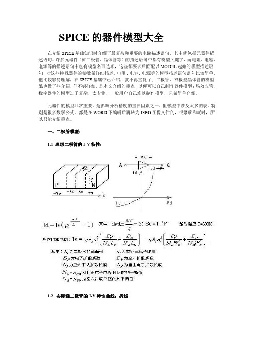
SPICE的器件模型大全在介绍SPICE基础知识时介绍了最复杂和重要的电路描述语句,其中就包括元器件描述语句。
许多元器件(如二极管、晶体管等)的描述语句中都有模型关键字,而电阻、电容、电源等的描述语句中也有模型名可选项,这些都要求后面配以.MODEL起始的模型描述语句,对这些特殊器件的参数做详细描述。
电阻、电容、电源等的模型描述语句语句比较简单,也比较容易理解,在SPICE基础中已介绍,就不再重复了;二极管、双极型晶体管的模型虽也做了些介绍,但不够详细,是本文介绍的重点,以便可以自己制作器件模型;场效应管、数字器件的模型过于复杂,太专业,一般用户自己难以制作模型,只做简单介绍。
元器件的模型非常重要,是影响分析精度的重要因素之一。
但模型中涉及太多图表,特别是很多数学公式,都是在WORD下编辑后再转为JEPG图像文件的,很繁琐和耗时,所以只能介绍重点。
一、二极管模型:1.1 理想二极管的I-V特性:1.2 实际硅二极管的I-V特性曲线:折线1.3 DC大信号模型:1.4 电荷存储特性:1.5 大信号模型的电荷存储参数Qd:1.6 温度模型:1.7 二极管模型参数表:二、双极型晶体管BJT模型:2.1 Ebers-Moll静态模型:电流注入模式和传输模式两种2.1.1 电流注入模式:2.1.2 传输模式:2.1.3 在不同的工作区域,极电流Ic Ie的工作范围不同,电流方程也各不相同:2.1.4 Early效应:基区宽度调制效应2.1.5 带Rc、Re、Rb的传输静态模型:正向参数和反向参数是相对的,基极接法不变,而发射极和集电极互换所对应的两种状态,分别称为正向状态和反向状态,与此对应的参数就分别定义为正向参数和反向参数。
2.2 Ebers-Moll大信号模型:2.3 Gummel-Pool静态模型:2.4 Gummel-Pool大信号模型:拓扑结构与Ebers-Moll大信号模型相同,非线性存储元件电压控制电容的方程也相同2.5 BJT晶体管模型总参数表:三、金属氧化物半导体晶体管MOSFET模型:3.1 一级静态模型:Shichman-Hodges模型3.2 二级静态模型(大信号模型):Meyer模型3.2.1 电荷存储效应:3.2.2 PN结电容:3.3 三级静态模型:3.2 MOSFET模型参数表:一级模型理论上复杂,有效参数少,用于精度不高场合,迅速粗略估计电路二级模型可使用复杂程度不同的模型,计算较多,常常不能收敛三级模型精度与二级模型相同,计算时间和重复次数少,某些参数计算比较复杂四级模型BSIM,适用于短沟道(<3um)的分析,Berkley在1987年提出四、结型场效应晶体管JFET模型:基于Shichman-Hodges模型4.1 N沟道JFET静态模型:4.2 JFET大信号模型:4.3 JFET模型参数表:五、 GaAs MESFET模型:分两级模型(肖特基结作栅极)GaAs MESFET模型参数表:六、数字器件模型:6.1 标准门的模型语句:.MODEL <(model)name> UGATE [模型参数]标准门的延迟参数:6.2 三态门的模型语句:.MODEL <(model)name> UTGATE [模型参数]三态门的延迟参数:6.3 边沿触发器的模型语句:.MODEL <(model)name> UEFF [模型参数] 边沿触发器参数:JKFF nff preb,clrb,clkb,j*,k*,g*,gb* JK触发器,后沿触发DFF nff preb,clrb,clk,d*,g*,gb* D触发器,前沿触发边沿触发器时间参数:6.4 钟控触发器的模型语句:.MODEL <(model)name> UGFF [模型参数] 钟控触发器参数:SRFF nff preb,clrb,gate,s*,r*,q*,qb* SR触发器,时钟高电平触发DLTCH nff preb,clrb,gate,d*,g*,gb* D触发器,时钟高电平触发钟控触发器时间参数:6.5 可编程逻辑阵列器件的语句:U <name> <pld type> (<#inputs>,<#outputs>) <input_node>* <output_node>#+<(timing model)name> <(io_model)name> [FILE=<(file name) text value>]+[DATA=<radix flag>$ <program data>$][MNTYMXDLY=<(delay select)value>] +[IOLEVEL=<(interface model level)value>]其中:<pld type>列表<(file name) text value> JEDEC格式文件的名称,含有阵列特定的编程数据JEDEC文件指定时,DATA语句数据可忽略<radix flag> 是下列字母之一:B 二进制O 八进制X 十六进制<program data> 程序数据是一个数据序列,初始都为0PLD时间模型参数:七、数字I/O接口子电路:数字电路与模拟电路连接的界面节点,SPICE自动插入此子电路子电路名(AtoDn和DtoAn)在I/O模型中定义,实现逻辑状态与电压、阻抗之间的转换。

第二章PSPICE使用本章通过对一个共射极放大电路的仿真分析,学习PSpice软件的使用方法,掌握PSpice 软件分析电子电路的基本过程。
使用PSpice软件的步骤是:第一步:通过电路图编辑程序(Schematics Editor程序)输入编辑电路图;第二步:在电路图编辑程序中设置电路的分析方式和参数;第三步:运行电路仿真分析程序(PSpice程序);第四步:运行图形后处理程序(Probe程序)查看输出图形或查看电路输出文件。
第一节认识Schematics电路图编辑程序一、启动Schematics程序PSpice软件7.1版本是Windows应用程序,因此,应先启动Windows操作系统,Windows 操作系统可以是Windows 3.x 或Windows 95或Windows 98,本书都是在Windows 98操作系统下完成的,并且假定读者已掌握Windows 98操作系统的使用,如果读者尚没有掌握Windows 98操作系统的使用,应先了解Windows 98操作系统;如果读者使用的是Windows 3.x 或Windows 95操作系统,则在Windows系统操作上会略有不同,但PSpice显示的内容都是一样的,相信不应该出现什么大的困难。
使用PSpice软件总是从输入电路图开始,除非你已经直接在电路描述文件中输入了电路所需的数据,因此,使用PSpice软件通常是从Schematics电路图编辑程序开始的。
而且在Schematics电路图编辑程序中可以设置电路的分析方式和参数,可以通过菜单命令启动电路仿真分析程序(PSpice程序)及图形后处理程序(Probe程序)。
假定已经安装了PSpice软件的7.1版本,并且已经启动了Windows 98操作系统,则启动Schematics电路图编辑程序有三种方法:1. 选择开始菜单上的程序组>>MicroSim Eval 7.1程序组>>Schamatics程序项。

PSpice中的模型和模型参数库一.PSpice中的模型参数库二.模型描述格式半导体器件模型描述格式子电路模型描述格式三.以已有模型为基础新建模型描述四.为实际元器件提取模型参数、建立模型描述3.模型类别(按照建模方式划分)(1) 元器件物理模型(2) 子电路宏模型(3) 黑匣子宏模型4. 目前研究的问题(1) 提高模型精度。
(2) 建立新器件的模型。
(3) 提高模型参数提取精度。
5.PSpice中的模型参数库(1) PSpice软件数据库中提供有三万多个元器件的模型参数;分别存放在一百多个模型参数库文件(扩展名为LIB);一.PSpice中的模型参数库5.PSpice中的模型参数库(1) PSpice软件数据库中提供有三万多个元器件的模型参数;分别存放在一百多个模型参数库文件(扩展名为LIB);每个模型参数库文件都对应有一个元器件符号库文件(以OLB为扩展名),存放不同元器件的符号图。
一.PSpice中的模型参数库5.PSpice中的模型参数库(1) PSpice软件数据库中提供有三万多个元器件的模型参数;分别存放在一百多个模型参数库文件(扩展名为LIB);每个模型参数库文件都对应有一个元器件符号库文件(以OLB为扩展名),存放不同元器件的符号图。
注意:这两类库文件存放的子目录不相同。
元器件符号库文件所在的路径元器件模型参数库文件所在的路径注意:只有上述库文件中的元器件符号才配置有模型参数一.PSpice中的模型参数库5.PSpice中的模型参数库(1) PSpice软件数据库中提供有三万多个元器件的模型参数;分别存放在一百多个模型参数库文件(扩展名为LIB);每个模型参数库文件都对应有一个元器件符号库文件(以OLB为扩展名),存放不同元器件的符号图。
注意:这两类库文件存放的子目录不相同。
(2) 用户绘制电路图时实际调用的是元器件符号库中的元器件符号图。
调用PSpice进行模拟仿真时软件自动从对应的模型参数库中调用相应的模型参数。
(3) 元器件符号与相应模型描述之间的“链接”关系:通过元器件符号图的参数设置指定这种“链接”关系。
选中元器件符号,执行快捷菜单中的Edit Part命令,打开Part Edit窗口,可以查看这种“链接”关系。
执行Option/Package Properties命令,出现Edit Part Properties对话框一.PSpice中的模型参数库5.PSpice中的模型参数库(1) PSpice软件数据库中提供有三万多个元器件的模型参数;分别存放在一百多个模型参数库文件(扩展名为LIB);每个模型参数库文件都对应有一个元器件符号库文件(以OLB为扩展名),存放不同元器件的符号图。
注意:这两类库文件存放的子目录不相同。
(2) 用户绘制电路图时实际调用的是元器件符号库中的元器件符号图。
调用PSpice进行模拟仿真时软件自动从对应的模型参数库中调用相应的模型参数。
(3) 元器件符号与相应模型描述之间的“链接”关系。
(4) 通过路径设置,引导模拟过程中PSpice查找到模型描述所在的模型参数库文件名及其路径名。
Nom.lib文件中包含了PSpice AD软件提供的所有模型参数库文件名称;Nom_aa.lib文件中包含了PSpice AA软件提供的所有模型参数库文件名称;如果用户自己建立了模型参数库文件,必须采用上述方法设置相应的库文件及其所在的路径名称。
否则PSpice在模拟时不知道如何查找相应的模型描述。
一.PSpice中的模型参数库6.模拟过程中在模型方面用户可能进行的工作(1) 查看模型和模型参数。
(2) 以已有的模型为基础新建模型。
(3) 为一个新的元器件提取模型参数。
(4) 用一个“元器件”代表一个电路单元甚至一个子系统。
这四项任务由Model Editor模块完成;一.PSpice中的模型参数库7. 模型库文件和模型的查阅-Model Editor(1) Model Editor模块的调用方法直接调用。
在Capture中调用:选中一个元器件,执行Edit/PSpice Model命令。
注意:如果需要在新建模型描述过程中同时为新建模型建立相应的元器件符号,必须采用“直接调用”的方式。
(2)查阅模型文件(3)查阅模型描述PSpice中的模型和模型参数库一.PSpice中的模型参数库二.模型描述格式半导体器件模型描述格式子电路模型描述格式三.以已有模型为基础新建模型描述四.为实际元器件提取模型参数、建立模型描述半导体器件模型描述格式半导体器件模型描述格式.MODEL<模型名称> <器件类型>+ ([<模型参数名称> = <模型参数值> [容差设置]])*模型参数描述语句各项含义:(1) .MODEL:关键词,表示这是一句元器件模型描述语句。
(2) 模型名称: 对应元器件描述语句中引用的“模型名称”。
(3) 器件类型: 说明该模型描述的是哪一类元器件的模型。
半导体器件模型描述格式.MODEL<模型名称> <器件类型>+ ([<模型参数名称> = <模型参数值> [容差设置]])*模型参数描述语句各项含义:(1) .MODEL:关键词,表示这是一句元器件模型描述语句。
(2) 模型名称: 对应元器件描述语句中引用的“模型名称”。
(3) 器件类型: 说明该模型描述的是哪一类元器件的模型。
(4) 模型参数名称: 不同元器件的每个模型参数都有规定的名称。
(5) 模型参数值:给相应模型参数的赋值。
若未指定,则采用默认值。
半导体器件模型描述格式.MODEL<模型名称> <器件类型>+ ([<模型参数名称> = <模型参数值> [容差设置]])*模型参数描述语句各项含义:(1) .MODEL:关键词,表示这是一句元器件模型描述语句。
(2) 模型名称: 对应元器件描述语句中引用的“模型名称”。
(3) 器件类型: 说明该模型描述的是哪一类元器件的模型。
(4) 模型参数名称: 不同元器件的每个模型参数都有规定的名称。
(5) 模型参数值:给相应模型参数的赋值。
若未指定,则采用默认值。
(6) 容差设置:采用下述格式指定该模型参数值的容差。
[DEV<独立变化值>[%]] [LOT<同步变化值>[%]]注意:DEV和LOT是关键词,描述容差变化的不同特点。
若给出%,则表示相对变化率,否则表示绝对变化值。
PSpice中的模型和模型参数库一.PSpice中的模型参数库二.模型描述格式半导体器件模型描述格式子电路模型描述格式三.以已有模型为基础新建模型描述四.为实际元器件提取模型参数、建立模型描述子电路模型描述格式1.子电路描述的基本格式(1) 预备知识-关于“电连接网表”作用:描述电路的拓扑连接关系以及每个元器件参数。
绘制好电路图后Pspice可以自动生成相应的电连接网表。
例:F007运算放大器的电路图。
子电路模型描述格式PSpice生成的F007电连接网表如下所示:Q_Q1 N00041 VI1 N00096 MOD1Q_Q2 N00041 VI2 N00122 MOD1Q_Q3 N00099 N00119 N00096 MOD2Q_Q4 N00125 N00119 N00122 MOD2…R_R8 N00198 VEE 50kR_R9 N00368 VEE 50kR_R10 N00480 VO 25kR_R11 VO N00466 50k每一条语句按照规定的格式描述一个元器件的编号名称、用节点号描述在电路中的连接关系、以及元件值或者器件模型名称。
在模型参数库中一定有一条模型描述语句描述该模型。
子电路模型描述格式1.子电路描述的基本格式(1) 预备知识-关于“电连接网表”(2) 子电路描述的作用在Pspice模型参数库中,每个集成电路元器件均采用子电路描述的方式说明该集成电路的等效电路结构。
F007内部电路图UA741等效电路图(采用受控源描述的“单元块”)UA741宏模型描述* 1:non-inverting input; 2:inverting input;* 3:positive power supply; 4:negative power ;5:output supply .subckt uA741 1 2 3 4 5q1 11 2 13 qxegnd99 0 poly(2),(3,0),(4,0) 0 .5 .5fb 7 99 poly(5) vb vc ve vlp vln 0 10.61E6 -1E3 1E3 10E6 -10E6ga 6 0 11 12 188.5E-6gcm 0 6 10 99 5.961E-9iee 10 4 dc 15.16E-6hlim 90 0 vlim 1K......vb 9 0 dc 0vc 3 53 dc 1ve 54 4 dc 1vlim 7 8 dc 0vlp 91 0 dc 40vln 0 92 dc 40.model qx NPN(Is=800.0E-18 Bf=93.75).endsPSpice中的模型和模型参数库一.PSpice中的模型参数库二.模型描述格式半导体器件模型描述格式子电路模型描述格式三.以已有模型为基础新建模型描述四.为实际元器件提取模型参数、建立模型描述注意几项参数设置应该选中此选项设置存放元器件符号的文件名和路径方式三.以已有模型为基础新建模型描述2.在已有的库文件中以已有模型为基础新建模型描述(1) 调用Model Editor模块;(2) 选择执行File/Open命令打开一个模型文件;(3) 选择执行Model/Copy From命令,设置有关参数。
三.以已有模型为基础新建模型描述(4) 完成图中设置后,点击图中OK按钮,当前打开的库文件中即新增一个名称为Q2N2222-MC的模型,屏幕上同时显示模型描述的具体内容,用户可进行修改。
(5) 在Model Editor中选择执行File/Save命令,更新已打开的库文件内容,将新建的模型添加到库文件中。
说明:按Tools/Options的设置,存放一个模型描述时,同时自动启动新建相应的元器件符号描述,其过程见下述第3个问题介绍。
三.以已有模型为基础新建模型描述3.以已有模型为基础将新建模型描述存放在用户定义的库文件中(1) 调用Model Editor模块;(2) 选择执行File/New命令,新建一个模型库文件;(3) 选择执行Model/Copy From命令,设置有关参数,包括修改模型参数描述的内容。
设置相关参数点击OK按钮在Model Editor窗口中出现新建器件模型描述用户可根据需要修改相应参数三.以已有模型为基础新建模型描述2.以已有模型为基础将新建模型描述存放在用户定义的库文件中(1) 调用Model Editor模块;(2) 选择执行File/New命令,新建一个模型库文件;(3) 选择执行Model/Copy From命令,设置有关参数,,包括修改模型参数描述的内容。