飞思卡尔面向智能移动设备市场推出MMA845xQ系列加速度传感器
- 格式:pdf
- 大小:74.77 KB
- 文档页数:1
分别列举10种接触、非接触传感器种类及原理接触式位移传感器:1位移传感器及其原理:计量光栅是利用光栅的莫尔条纹现象来测量位移的。
“莫尔”原出于法文Moire,意思是水波纹。
几百年前法国丝绸工人发现,当两层薄丝绸叠在一起时,将产生水波纹状花样;如果薄绸子相对运动,则花样也跟着移动,这种奇怪的花纹就是莫尔条纹。
一般来说,只要是有一定周期的曲线簇重叠起来,便会产生莫尔条纹。
计量光栅在实际应用上有透射光栅和反射光栅两种;按其作用原理又可分为辐射光栅和相位光栅;按其用途可分为直线光栅和圆光栅。
下面以透射光栅为例加以讨论。
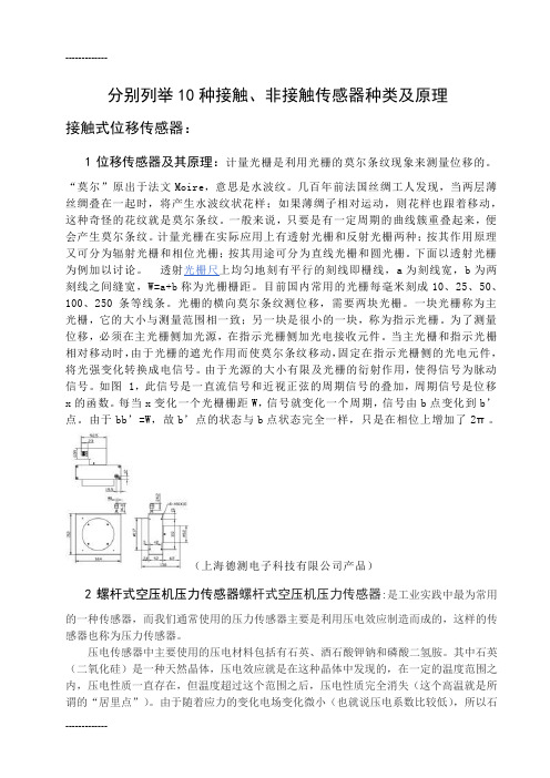
透射光栅尺上均匀地刻有平行的刻线即栅线,a为刻线宽,b为两刻线之间缝宽,W=a+b称为光栅栅距。
目前国内常用的光栅每毫米刻成10、25、50、100、250条等线条。
光栅的横向莫尔条纹测位移,需要两块光栅。
一块光栅称为主光栅,它的大小与测量范围相一致;另一块是很小的一块,称为指示光栅。
为了测量位移,必须在主光栅侧加光源,在指示光栅侧加光电接收元件。
当主光栅和指示光栅相对移动时,由于光栅的遮光作用而使莫尔条纹移动,固定在指示光栅侧的光电元件,将光强变化转换成电信号。
由于光源的大小有限及光栅的衍射作用,使得信号为脉动信号。
如图 1,此信号是一直流信号和近视正弦的周期信号的叠加,周期信号是位移x的函数。
每当x变化一个光栅栅距W,信号就变化一个周期,信号由b点变化到b’点。
由于bb’=W,故b’点的状态与b点状态完全一样,只是在相位上增加了2π。
(上海德测电子科技有限公司产品)2螺杆式空压机压力传感器螺杆式空压机压力传感器:是工业实践中最为常用的一种传感器,而我们通常使用的压力传感器主要是利用压电效应制造而成的,这样的传感器也称为压力传感器。
压电传感器中主要使用的压电材料包括有石英、酒石酸钾钠和磷酸二氢胺。
其中石英(二氧化硅)是一种天然晶体,压电效应就是在这种晶体中发现的,在一定的温度范围之内,压电性质一直存在,但温度超过这个范围之后,压电性质完全消失(这个高温就是所谓的“居里点”)。
© 2010, 2012 Freescale Semiconductor, Inc. All rights reserved.Document Number: AN4074Rev 1, 03/2012Freescale Semiconductor Application NoteAuto-Wake/Sleep Using the MMA8451, 2, 3Qby: Kimberly TuckApplications Engineer1.0IntroductionAccelerometers are commonly used in hand-held electronics and/or battery operated electronic devices.Consumption of current in the entire system is a critical feature of the product design. Users do not want to be inconvenienced by continually recharging or changing out batteries. When designing in the accelerometer, battery power usage is often a critical feature which concerns many designers.Therefore, current consumption of the sensor as well as of the entire system should be paramount design considerations. If the system processor is used often only for processing data from the accelerometer, then it is ideal to embed the intelligence in the sensor to avoid burdening the system processor from running continually. The flexibility ofembedded interrupt driven functions and selectable data rates with trade-offs for resolution, response time, and current are the types of intelligent features in the MMA8451, 2, 3Q.This application note will explain the following:•The Auto-Wake/Sleep feature•Description of the configuration procedure withexample register settings and code.1.1Key WordsAccelerometer, Output Data Rate (ODR), Current, Standby Current, Power Down Mode Current, Low Power Mode, Noise, Auto-Wake/Sleep, Sleep Timer, Sensor.TABLE OF CONTENTS1.0 Introduction . . . . . . . . . . . . . . . . . . . . . . . . . . . . . . . . . . . . . . . . . . . . . . . . .11.1 Key Words . . . . . . . . . . . . . . . . . . . . . . . . . . . . . . . . . . . . . . . . . . . . . . . . . . .11.2 Summary . . . . . . . . . . . . . . . . . . . . . . . . . . . . . . . . . . . . . . . . . . . . . . . . . . . .22.0 MMA8451, 2, 3Q Consumer 3-axis Accelerometer 3 by 3 by 1 mm. . . . .22.1 Output Data, Sample Rates and Dynamic Ranges of all Three Products . . .22.1.1 MMA8451Q . . . . . . . . . . . . . . . . . . . . . . . . . . . . . . . . . . . . . . . . . . . . . .22.1.2 MMA8452Q . . . . . . . . . . . . . . . . . . . . . . . . . . . . . . . . . . . . . . . . . . . . . .22.1.3 MMA8453Q Note: No HPF Data . . . . . . . . . . . . . . . . . . . . . . . . . . . . . . .23.0 Configuring the MMA8451, 2, 3Q into Auto-Wake/Sleep Mode . . . . . . . .33.1 Set the Sleep Enable Bit . . . . . . . . . . . . . . . . . . . . . . . . . . . . . . . . . . . . . . . . .43.2 Set the Sleep Mode and Wake Mode Oversampling Mode. . . . . . . . . . . . . . .43.3 Configure the Sleep Sample Rate and Wake Sample Rate . . . . . . . . . . . . . .53.4 Set the Timeout Counter . . . . . . . . . . . . . . . . . . . . . . . . . . . . . . . . . . . . . . . . .53.5 Enable the Interrupts to be used in the System and Route to INT1 or INT2. . . . . . . . . . . . . . . . . . . . . . . . . . . . . . . . . . . . . . . . . . . . . . . . . . . . . . . . . . . .63.6 Enable the Interrupt Sources that Wake the Device . . . . . . . . . . . . . . . . . . . .64.0 Example Configuration for the Auto-Wake/Sleep Function. . . . . . . . . . .7Table 14.Registers used for Auto-Wake/Sleep Functionality. . . . . . . . . . . . . . . .74.1 Example Procedure for Configuring the Auto-Wake/Sleep Function Conditions. . . . . . . . . . . . . . . . . . . . . . . . . . . . . . . . . . . . . . . . . . . . . . . . . . . . . . . . . . . .8AN4074Sensors1.2SummaryThe MMA845xQ can be used to cycle between different ODRs, which results in overall lower current consumption of the device. This can be achieved from several programmable functions.2.0MMA8451, 2, 3Q Consumer 3-axis Accelerometer 3 by 3 by 1 mmThe MMA8451, 2, 3Q has a selectable dynamic range of ±2g, ±4g, ±8g. The device has 8 different output data rates, selectable high pass filter cut-off frequencies, and high pass filtered data. The available resolution of the data and the embedded features is dependant on the specific device.Note: The MMA8450Q has a different memory map and has a slightly different pinout configuration.Figure 1. MMA8451, 2, 3Q Consumer 3-axis Accelerometer 3 by 3 by 1 mm2.1Output Data, Sample Rates and Dynamic Ranges of all Three Products2.1.1MMA8451Q1.14-bit data2g (4096 counts/g = 0.25 mg/LSB) 4g (2048 counts/g = 0.5 mg/LSB) 8g (1024 counts/g = 1 mg/LSB)2.8-bit data2g (64 counts/g = 15.6 mg/LSB) 4g (32 counts/g = 31.25 mg/LSB) 8g (16 counts/g = 62.5 mg/LSB)3.Embedded 32 sample FIFO (MMA8451Q)2.1.2MMA8452Q1.12-bit data2g (1024 counts/g = 1 mg/LSB) 4g (512 counts/g = 2 mg/LSB) 8g (256 counts/g = 3.9 mg/LSB)2.8-bit data2g (64 counts/g = 15.6 mg/LSB) 4g (32 counts/g = 31.25 mg/LSB) 8g (16 counts/g = 62.5 mg/LSB)2.1.3MMA8453Q Note: No HPF Data1.10-bit data2g (256 counts/g = 3.9 mg/LSB) 4g (128 counts/g = 7.8 mg/LSB) 8g (64 counts/g = 15.6 mg/LSB)2.8-bit data2g (64 counts/g = 15.6 mg/LSB) 4g (32 counts/g = 31.25 mg/LSB) 8g(16 counts/g = 62.5 mg/LSB)12345910111213141516876N CV D DN CVDDIO BYP NC SCL GNDNC GND INT1GND INT2S A 0N CS D AMMA845xQ 16-Pin QFN (Top View)AN4074Sensors3.0Configuring the MMA8451, 2, 3Q into Auto-Wake/Sleep ModeThe MMA8451, 2, 3Q can be configured to transition between different sample rates (different current consumption) based on different selected events. Enabling this feature can be accomplished by enabling the Sleep Mode and setting a timeout period. Then the functions of interest must be set to trigger the device to wake. Both Wake and Sleep are considered “Active” Modes because data and interrupts are available. The difference between the modes is that the sample rate in Sleep Mode is limited to a maximum of 50 Hz. The advantage of using the Auto-Wake/Sleep is that the system can automatically transition to a higher sample rate (higher current consumption) when needed but spends the majority of the time in the Sleep Mode (lower current) when the device does not require higher sampling rates. This can all be triggered on selected events. The Low Noise bit (Register 0x2A bit 2) can be used as well with this feature. Be aware that using the Low Noise bit will limit the dynamic range to 4g, regardless of the set range of the full scale value. The oversampling mode can also be changed from Active Sleep Mode to Active Wake Mode. The Sleep Mode oversampling option is set in Register 0x2B using bit 3 and bit 4 SMODS0 and SMODS1. The Active Wake Mode oversampling option is set in Register 0x2B using bit 0 and bit 1 MODS0 and MODS1. For example the device can be configured to be in Low Power Mode when asleep at 1.56 Hz to be in the lowest current consumption configuration. Then the device can be set for High Resolution Mode at 6.25 Hz when awake to be prepared to take higher resolution data for a tilt application.Figure 2 shows transition states from the Wake, Sleep and Standby modes.Figure 2. Mode TransitionsTable 1 compares how the current consumption changes with the data rate and with the oversampling mode chosen. The over-sampling modes are “Normal”, “Low Noise and Low Power”, “High Resolution” and “Low Power”. The oversampling ratios are given at each data rate along with the current consumption values for each. The more averaging done internally results in higher current consumption. Note the Low Power Mode has the least amount of averaging and the lowest current consumption.Table 2 shows the list of functions that will delay the device from returning to sleep and waking from sleep. Note that the MMA8451Q is the only device that contains the FIFO. The FIFO can delay the device from going to sleep but it is not capable of waking the device from sleep. The transient, portrait/landscape, tap, and motion/freefall functions can all delay the device from sleep by servicing the interrupt before the timeout period. They can also wake the device from sleep. The Auto-Sleep interrupt indicates when the device changes modes from Wake to Sleep or Sleep to Wake but the interrupt does not affect the state change. Also the data ready interrupt does not affect the state change from the Wake to Sleep or Sleep to Wake state.Table 1. (S)MODS Oversampling Options with Current Consumption ValuesMode ODR NormalLow Noise and Low Power High Resolution Low PowerCurrent μAOS RatioCurrent μAOS RatioCurrent μAOS RatioCurrent μAOSRatio8001652165216521652400165416541654852200854854165844210044444416516242502442441653214212.5241684165128626.25243288165256641.5625241288321651024616StandbySYSMOD[1:0] = 00WakeSYSMOD[1:0] = 01<DR>SleepSYSMOD[1:0] = 10A SLP_RATE[1:0]I n t e r r u p t s If Time > ASLP_COUNT[7:0] and no Interrupts triggeredt r i g g e r e dAN4074SensorsNote that to configure the Auto-Wake/Sleep functionality, the selected embedded functions must be enabled (Register 0x2D) and the same corresponding functions must be set to “Wake-from-Sleep” (Register 0x2C) if they are to be used to wake the de-vice.All enabled functions will still function in Sleep Mode at the sleep ODR. Only the functions that have been selected for “Wake-from-Sleep” will wake the device. If nothing is selected to Wake-from-Sleep then the device will remain in Sleep Mode and will never wake up.This section reviews the different registers involved in configuring the device for auto-wake/sleep.1.Register 0x2B bit 2 – SLPE Enable Sleep bit2.Register 0x2B Set the Sleep Mode Oversampling Rate3.Register 0x2A Sleep Sample Rate and Wake Sample Rate4.Register 0x29 Timeout Counter5.Register 0x2D Enable the Interrupts for the Selected Functions6.Register 0x2E Route the Interrupts to INT1 or INT27.Register 0x2C Enable the Wake-from-Sleep Interrupts3.1Set the Sleep Enable BitIf the Sleep Enable bit (Register 0x2B bit 2) is NOT enabled then the device can only toggle between Standby and Wake Mode by writing to the Active bit in Register 0x2A. When the Sleep Enable bit is enabled the device can transition between Standby, Wake, and Sleep. The SLPE bit is shown as bit 2 in Table 4.3.2Set the Sleep Mode and Wake Mode Oversampling ModeThere are four different oversampling modes described in Table 3 They are “Normal”, “Low Noise and Low Power”, “High Res-olution” and “Low Power”. The oversampling mode changes the current consumption, resolution and also the debounce counter timers in the part. The device can be configured to be in Low Power Mode while in Sleep and then to Normal Mode when awake or any of the other fifteen combinations. This allows for further current savings in the Sleep Mode. The different bit settings are shown in Table 3. The Wake oversampling modes configured from bit 0 and bit 1 in Register 0x2B. The Sleep oversampling modes are configured from bit 3 and bit 4 in SMODS in Register 0x2B.Table 2. Interrupt Sources and the effects on the state change from Wake to Sleep and Sleep to Wake ModesInterrupt Source Event Restarts Timer and Delays Return-to-SleepEvent will Wake-from-SleepFIFO_GATE Yes No SRC_TRANS Yes Yes SRC_LNDPRT Yes Yes SRC_PULSE Yes Yes SRC_FF_MT Yes Yes SRC_ASLP No No SRC_DRDYNoNoTable 3. Settings for Oversampling Modes(S)MODS1(S)MODS0Power Mode 00Normal01Low Noise and Low Power10High Resolution 11Low PowerTable 4. 0x2B CTRL_REG2 Register (Read/Write) and DescriptionBit 7Bit 6Bit 5Bit 4Bit 3Bit 2Bit 1Bit 0STRSTSMODS1SMODS0SLPEMODS1MODS03.3Configure the Sleep Sample Rate and Wake Sample RateIt is important to note that when the device is in Sleep Mode, the system ODR is overwritten by the data rate set by the ASLP_RATE field in the CTRL_REG1 Register (0x2A). The Sleep Sample Rate (ASLP_RATE[0:1]) and the Wake Mode Sample Rate (DR[0:3]) are found in Table 5. The different bit settings for the Sleep Mode Sample Rate can be found in Table 6. The bit settings for the Wake Mode Sample Rates are found in Table 7.Table 5. 0x2A CTRL_REG1 Register (Read/Write) and DescriptionBit 7Bit 6Bit 5Bit 4Bit 3Bit 2Bit 1Bit 0 ASLP_RA TE1ASLP_RA TE0DR2DR1DR0LNOISE F_READ ACTIVETable 6. Sleep Mode Sample Rate DescriptionASLP_RATE1ASLP_RATE0ODR Period0050 Hz20 ms0112.5 Hz80 ms10 6.25 Hz160 ms11 1.56 Hz640 msTable 7. Wake Mode Sample Rate DescriptionDR2DR1DR0ODR Period000800.0 Hz 1.25 ms001400.0 Hz 2.5 ms010200.0 Hz 5 ms011100.0 Hz10 ms10050.0 Hz20 ms10112.5 Hz80 ms110 6.25 Hz160 ms111 1.56 Hz640 ms3.4Set the Timeout CounterThe ASLP_COUNT Register 0x29 shown in Table 8 sets the minimum time period of inactivity required to change the current ODR value from the value specified in the DR[2:0] to that in the ASLP_RATE[1:0] (Register 0x2A). Of course this only occurs provided the SLPE bit is set.Table 8. 0x29 ASLP_COUNT Register (Read/Write) and DescriptionBit 7Bit 6Bit 5Bit 4Bit 3Bit 2Bit 1Bit 0 D7D6D5D4D3D2D1D0 D7-D0 defines the minimum duration time to change current ODR value from DR to ASLP_RATE. Time step and maximum value depend on the ODR chosen. See Table 9.Table 9. ASLP_COUNT Relationship with ODROutput Data Rate (ODR)Duration ODR Time Step ASLP_COUNT Step8000 to 81s 1.25 ms320 ms4000 to 81s 2.5 ms320 ms2000 to 81s 5 ms320 ms1000 to 81s10 ms320 ms500 to 81s20 ms320 ms12.50 to 81s80 ms320 ms6.250 to 81s160 ms320 ms1.560 to 162s640 ms640 msAN4074 SensorsAN4074Sensors3.5Enable the Interrupts to be used in the System and Route to INT1 or INT2The interrupt functions must be enabled in Register 0x2D per Table 10 for the event to trigger the Auto-Wake/Sleep. The func-tions must also be configured with the appropriate thresholds and timing values to detect the events.The corresponding interrupt enable bit allows the function to route its event detection flag to the interrupt controller. The inter-rupt controller routes the enabled interrupt to the INT1 or INT2 pin. By default all interrupts are routed to INT2 and the correspond-ing configuration register bit value is 0. To route a functional block to INT1 instead of the default, set the corresponding configuration register bit to 1. The configuration register bit settings are shown in Table 11.3.6Enable the Interrupt Sources that Wake the DeviceThe register to control which interrupts will wake the device are configured in Register 0x2C shown in Table 12. There are five (5) functions that can be used to keep the sensor from falling asleep if they are enabled. These are the Transient, Orien-tation, Tap, Motion/FF and the FIFO. There are only four (4) functions used to wake the device. The FIFO will not wake the device from sleep. Also note the Auto-Wake/Sleep interrupt and the data ready interrupt do not affect the Wake/Sleep. Note that the FIFO is only available in the MMA8451Q device.Note: The FIFO is flushed whenever the system ODR changes in order to prevent mixing the FIFO data from different time domains unless the FIFO_GATE (bit 7) is set. Also, the FIFO cannot wake the device from sleep but can prevent the device from going to sleep. Details of the functionality of the FIFO is captured in Table 13.Table 10. Register 0x2D CTRL_REG4 Register (Read/Write) and DescriptionBit 7Bit 6Bit 5Bit 4Bit 3Bit 2Bit 1Bit 0INT_EN_ASLPINT_EN_FIFOINT_EN_TRANSINT_EN_LNDPRTINT_EN_PULSEINT_EN_FF_MT—INT_EN_DRDYTable 11. Register 0x2E CTRL_REG5 Register (Read/Write) and DescriptionBit 7Bit 6Bit 5Bit 4Bit 3Bit 2Bit 1Bit 0INT_CFG_ASLPINT_CFG_FIFOINT_CFG_TRANS INT_CFG_LNDPRT INT_CFG_PULSE INT_CFG_FF_MT—INT_CFG_DRDYTable 12. Register 0x2C CTRL_REG3 Interrupt Control Register and DescriptionBit 7Bit 6Bit 5Bit 4Bit 3Bit 2Bit 1Bit 0FIFO_GA TEWAKE_TRANS WAKE_LNDPRT WAKE_PULSEWAKE_FF_MT—IPOLPP_ODTable 13. Behavior of FIFO under Wake/Sleep ConditionsFIFO INT EnabledWake-from-SleepEnabledResultNO NOFIFO will fall asleep when the sleep timer times out and no other interrupt wakes the system.There is an AUTOMATIC flush and the FIFO starts refilling at the Sleep ODR from 0.If another functional block causes the device to wake the FIFO will FLUSH itself again and start filling at the Wake ODR.YES NOWith the interrupt enabled the FIFO can be read and flushed clearing the interrupt. The system is kept from falling asleep by reading the status after the interrupt is set. The FIFO does not have to be flushed to keep the device in Wake Mode- as long as the FIFO status is read continuously after the FIFO interrupt is enabled. If the system falls asleep (and no new interrupts occur during the timeout period), the FIFO AUTOMATICALLY flushes and starts refilling at the Sleep ODR from 0 and stores at the Wake ODR.NO YESFIFO will fall asleep if no wake events occur within the timeout st data remains here in the FIFO until it is flushed.Once the FIFO is flushed, it will start collecting the new data at the current ODR.YES YESWith interrupt enabled, the FIFO can be read and flushed (clearing the interrupt) . Note: Reading the FIFO status will keep the system from falling asleep.If the system does fall asleep (and no interrupts occur during the timeout period) then the FIFO will stop collecting any data. The last data will be held in the FIFO.Once the FIFO is flushed, it will start collecting the new data at the current ODR.AN4074Sensors4.0Example Configuration for the Auto-Wake/Sleep FunctionThe following are the steps to configure the Auto-Wake/Sleep function with the registers of importance in Table 14. In this ex-ample, the data rate will be set to 100 Hz in Wake Mode and 6.25 Hz in Sleep Mode. The Oversampling Mode will be set to High Resolution in the Wake Mode and Low Power Mode in Sleep Mode. The timeout period will be set to 20 seconds. The wake triggers will be tap and motion. There may be other interrupts that are enabled in the system including orientation detection, but these will not wake the device in this example.Table 14. Registers used for Auto-Wake/Sleep FunctionalityReg Name Definition Bit 7Bit 6Bit 5Bit 4Bit 3Bit 2Bit 1Bit 00B SYSMOD System ModeR FGERR FGT_4FGT_3FGT_2FGT_1FGT_0SYSMOD1SYSMOD00C INT_SOURCE Interrupt StatusR SRC_ASLPSRC_FIFOSRC_TRANSSRC_LNDPRTSRC_PULSESRC_FF_MT—SRC_DRDY29ASLP_COUNT Auto-Sleep CounterR/W D7D6D5D4D3D2D1D02A CTRL_REG1Control Reg1R/W ASLP_RATE1ASLP_RATE0DR2DR1DR0LNOISE F_READ ACTIVE 2BCTRL_REG2Control Reg2R/W STRSTSMODS1SMODS0SLPEMODS1MODS02C CTRL_REG3Control Reg3R/W(Wake Interrupts fromSleep)FIFO_GATE WAKE_TRANS WAKE_LNDPRT WAKE_PULSE WAKE_FF_MT —IPOL PP_OD2D CTRL_REG4Control Reg4R/W(Interrupt Enable Map)INT_EN_ASLP INT_EN_FIFO INT_EN_TRANS INT_EN_LNDPRT INT_EN_PULSE INT_EN_FF_MT —INT_EN_DRDY2E CTRL_REG5Control Reg5R/W(Interrupt Configuration)INT_CFG_ASLP INT_CFG_FIFO INT_CFG_TRANS INT_CFG_LNDPRT INT_CFG_PULSE INT_CFG_FF_MT —INT_CFG_DRDY4.1Example Procedure for Configuring the Auto-Wake/Sleep Function Conditions•Dynamic Range = 2g•Sleep Timeout period = 20 seconds•Wake Triggers = Tap and Motion•Wake Sample Rate = 100 Hz,•Wake Oversampling Mode = High Resolution•Sleep Sample Rate = 6.25 Hz•Sleep Oversampling Mode = Low PowerStep 1:Put the device in Standby ModeRegister 0x2A CTRL_REG1CTRL_REG1_Data = IIC_RegRead(0x2A);CTRL_REG1_Data& = 0xFE; //Clear Active BitIIC_RegWrite(0x2A,CTRL_REG1_Data);Step 2:To enable the Auto-Wake/Sleep set bit 2 in Register 0x2B, the SLPE bit.Register 0x2B CTRL_REG2CTRL_REG2_Data = IIC_RegRead(0x2B); //Store value in the RegisterCTRL_REG2_Data| = 0x04; //Set the Sleep Enable bitIIC_RegWrite(0x2B, CTRL_REG2_Data); //Write the updated value into CTRL_REG2.Step 3:The sleep sample rate must be chosen by writing in the corresponding sample rate value to bits6 and7 ASLP_RATE0 and ASLP_RATE1 (01) and the Wake Sample rate bits 5, 4 and 3 to DR(011) in Register 0x2A.Register 0x2A CTRL_REG1 ASLP_RATE = 01 (6.25 Hz), DR = 011(100 Hz)CTRL_REG1_Data = IIC_RegRead(0x2A);CTRL_REG1_Data& = 0x5E; //clear the bits that should be cleared for the sample ratesCTRL_REG1_Data| = 0x58; //Set ASLP = 6.25 Hz, DR = 100 HzIIC_RegWrite(0x2A,CTRL_REG1_Data);Step 4:Set the Wake Oversampling Mode to High Resolution (10) and the Sleep Oversampling Mode to Low Power (11)CTRL_REG2_Data = IIC_RegRead(0x2B);CTRL_REG2_Data& = 0xE4; //puts both Oversampling modes in Normal ModeCTRL_REG2_Data| = 0x1A; //Wake High Res, Sleep Low PowerIIC_RegWrite(0x2B,CTRL_REG2_Data);Step 5:The Interrupt for the event to trigger the device to wake up must be enabled by writing to Register 0x2D, CTRL_Reg4. Bits 2 through 7 will affect the Auto-Wake/sleep. The data readyinterrupt doesn’t trigger the Auto-Wake/Sleep mechanism.Example: Set Pulse and Orientation and Motion 1 and Auto-Wake/Sleep InterruptsEnabled in the SystemIIC_RegWrite(0x2D, 0x9C);Step 6:Route the interrupt chosen and enabled to either INT1 or INT2 in Register 0x2E CTRL_REG5.Example: Route Pulse, Motion1 and Orientation to INT2 and Auto-Sleep to INT1.IIC_RegWrite(0x2E,0x80);Step 7:Enable the interrupts that will wake the device from sleep. There can be more interrupts enabled in Step 4 than in Step 6. Only interrupts that are Enabled in Step 4 and that have the “Wake-from-Sleep” bit set in Register 0x2C will actually wake the device.Example: Choose Pulse and Motion to wake the device from sleepIIC_RegWrite(0x2C,0x18);AN4074SensorsStep 8:Set the Dynamic Range to 2gRegister 0x0E XYZ_DATA_CFGXYZ_CFG_Data = IIC_RegRead(0x0E);XYZ_CFG_Data & = 0xFC; //Clear the FS bits to 00 2gIIC_RegWrite(0x0E, XYZ_CFG_Data);Step 9:Write an Interrupt Service routine to monitor the Auto-Sleep InterruptInterrupt void isr_KBI (void){//clear the interrupt flagCLEAR_KBI_INTERRUPT;//Determine the source of interrupt by reading the system interrupt registerInt_SourceSystem = IIC_RegRead(0x0C);//Set up Case statement here to service all of the possible interruptsif ((Int_SourceSystem &=0x80)==0x80){//Perform an Action since Auto-Sleep Flag has been set//Read the System Mode to clear the system interruptInt_SysMod = IIC_RegRead(0x0B);if (Int_SysMod==0x02){//sleep mode}else if (Int_SysMod==0x01){//Wake Mode}else{//Error}}}Related DocumentationThe MMA845xQ device features and operations are described in a variety of reference manuals, user guides, and application notes. To find the most-current versions of these documents:1.Go to the Freescale homepage at:/2.In the Keyword search box at the top of the page, enter the device number MMA845xQ.3.In the Refine Your Result pane on the left, click on the Documentation link.AN4074 SensorsHow to Reach Us:Home Page:Web Support:/supportUSA/Europe or Locations Not Listed: Freescale Semiconductor, Inc. Technical Information Center, EL516 2100 East Elliot RoadTempe, Arizona 852841-800-521-6274 or +1-480-768-2130 /supportEurope, Middle East, and Africa:Freescale Halbleiter Deutschland GmbHTechnical Information CenterSchatzbogen 781829 Muenchen, Germany+44 1296 380 456 (English)+46 8 52200080 (English)+49 89 92103 559 (German)+33 1 69 35 48 48 (French)/supportJapan:Freescale Semiconductor Japan Ltd.HeadquartersARCO Tower 15F1-8-1, Shimo-Meguro, Meguro-ku,Tokyo 153-0064Japan0120 191014 or +81 3 5437 9125support.japan@Asia/Pacific:Freescale Semiconductor China Ltd.Exchange Building 23FNo. 118 Jianguo RoadChaoyang DistrictBeijing 100022China+86 10 5879 8000@For Literature Requests Only:Freescale Semiconductor Literature Distribution Center 1-800-441-2447 or +1-303-675-2140Fax: +1-303-675-2150 LDCForFreescaleSemiconductor@AN4074Information in this document is provided solely to enable system and software implementers to use Freescale Semiconductor products. There are no express or implied copyright licenses granted hereunder to design or fabricate any integrated circuits or integrated circuits based on the information in this document.Freescale Semiconductor reserves the right to make changes without further notice to any products herein. Freescale Semiconductor makes no warranty, representation or guarantee regarding the suitability of its products for any particular purpose, nor does Freescale Semiconductor assume any liability arising out of the application or use of any product or circuit, and specifically disclaims any and all liability, including without limitation consequential or incidental damages. “Typical” parameters that may be provided in Freescale Semiconductor data sheets and/or specifications can and do vary in different applications and actual performance may vary over time. All operating parameters, including “Typicals”, must be validated for each customer application by customer’s technical experts. Freescale Semiconductor does not convey any license under its patent rights nor the rights of others. Freescale Semiconductor products are not designed, intended, or authorized for use as components in systems intended for surgical implant into the body, or other applications intended to support or sustain life, or for any other application in which the failure of the Freescale Semiconductor product could create a situation where personal injury or death may occur. Should Buyer purchase or use Freescale Semiconductor products for any such unintended or unauthorized application, Buyer shall indemnify and hold Freescale Semiconductor and its officers, employees, subsidiaries, affiliates, and distributors harmless against all claims, costs, damages, and expenses, and reasonable attorney fees arising out of, directly or indirectly, any claim of personal injury or death associated with such unintended or unauthorized use, even if such claim alleges that Freescale Semiconductor was negligent regarding the design or manufacture of the part. Freescale and the Freescale logo are trademarks of Freescale Semiconductor, Inc., Reg. U.S. Pat. & Tm. Off. The Energy Efficiency Solutions Logo and Xtrinsic are trademarks of Freescale Semiconductor, Inc.All other product or service names are the property of their respective owners.© 2012 Freescale Semiconductor, Inc. All rights reserved.。


飞思卡尔新的Xtrinsic六轴传感器丰富了移动设备的功能
目前先进的移动操作系统要求
使用先进的传感器技术来提
供更准确的数据
飞思卡尔副总裁兼传感器与制
Seyed
轴
并采用
将这些数据融合在一
,
准确地做在一台设备中集成多个传感可降低开发整套系统解决方案的帮助开发人员缩短产品上市最近推出的面向基于Windows®8操作
系统的便携式设备的Xtrinsic 12轴传感
器融合平台,以及Xtrinsic eCompass传
感器融合软件。
Xtrinsic 6轴传感器特性
Xtrinsic FXOS8700CQ 6轴传感器采
用3×3mm封装,其中包含一个 14位加
速计和16位磁力计,以及一个高性能
的 ASIC。
这种高性能的eCompass解决
方案能够为大多数应用提供分辨率在
0.1度、误差低于5度的航向精确度。
于2012
销合作伙伴进行批量销售
价格:
美元。
飞思卡尔传感器工具箱
To ol b
面向加速计
和触摸
件。
飞思卡尔计划于第三季度供应
LFSTBEB8700
为75美元
Xtrinsic FXOS8700 6。