飞思卡尔加速度传感器资料AN4074 MMA8451Q Auto-Wake Sleep
- 格式:pdf
- 大小:188.20 KB
- 文档页数:10

飞思卡尔通过为消费应用量身定制的功能扩展模拟加速计产品
系列
佚名
【期刊名称】《电子与电脑》
【年(卷),期】2008(000)006
【摘要】加速计正日益成为需要低功耗、先进的移动传感和小巧外形的消费应用的主流技术。
飞思卡尔半导体成功扩展了其低重力三轴模拟加速计产品系列,以顺应消费电子市场上的这一趋势。
MMA7361L、MMA7368L、MMA7341L和MMA7331L三轴模拟加速计带有专为手机、硬盘、媒体播放器、游戏和玩具移动传感设计的特性。
【总页数】1页(P63)
【正文语种】中文
【中图分类】TP393
【相关文献】
1.可为客户量身定制飞思卡尔推出高精度锂电池充电器IC [J], 飞思卡尔半导体
2.飞思卡尔Xtrinsic加速计延长消费电子器件的电池使用寿命 [J],
3.可为客户量身定制飞思卡尔推出高精度锂电池充电器IC [J],
4.可为客户量身定制飞思卡尔推出高精度锂电池充电器IC [J], 周鑫
5.为客户量身定制飞思卡尔推出锂电池充电器IC [J], 飞思卡半导体
因版权原因,仅展示原文概要,查看原文内容请购买。
7.0 14位,12位或10位数据流和数据转换MMA8451Q具有14位的XYZ数据。
MMA8452Q具有12位XYZ数据而MMA8453具有10位的数据。
本节概述了如何根据不同的MCU以及不同的数据格式来处理这些不断产生的14位数据数据。
“示例将以14位数据为例给出,但读者可以理解对于12位数据或10位数据应当作出怎样的变化。
驱动程序代码具有所有的数据格式的所有功能。
事件标志可以通过读状态寄存器(0×00)来监视。
监视事件标志可以通过本文件的第9.0节中所讨论的轮询或中断技术来完成。
完全没有必要读状态寄存器来将其清除。
读取数据将会清除状态寄存器。
表9。
0X00 状态寄存器:数据状态寄存器(只读)每当有新的数据在任何轴出现时,ZYXDR标志将被置位。
下面的示例代码演示了如何监视这个标志位,当检测到新的数据时,通过一个单次的多字节I2C访问,将14/12/10-bit的XYZ数据读取到RAM中的一个数组(value[])。
然后这些值被复制到16-bit变量以进行进一步加工。
Code Example:/*** Poll the ZYXDR status bit and wait for it to set.*/RegisterFlag.Byte = IIC_RegRead(STATUS_00_REG);if (RegisterFlag.ZYXDR_BIT == 1){/*** Read 14/12/10-bit XYZ results using a 6 byte IIC access.*/IIC_RegReadN(OUT_X_MSB_REG, 6, &value[0]);/*** Copy and save each result as a 16-bit left-justified value.*/x_value.Byte.hi = value[0];x_value.Byte.lo = value[1];y_value.Byte.hi = value[2];y_value.Byte.lo = value[3];z_value.Byte.hi = value[4];z_value.Byte.lo = value[5];}下面的例子展示了一个与寄存器对应的左对齐的16bit X轴数据结果表10。

MMA8453QRev 3, 10/2010Freescale Semiconductor Technical DataAn Energy Efficient Solution by Freescale3-Axis, 10-bit/8-bitDigital AccelerometerThe MMA8453Q is a smart low-power, three-axis, capacitive micromachined accelerometer with 10 bits of resolution. This accelerometer is packed withembedded functions with flexible user programmable options, configurable to two interrupt pins. Embedded interrupt functions allow for overall power savings relieving the host processor from continuously polling data.The MMA8453Q has user selectable full scales of ±2g/±4g/±8g. The device can be configured to generate inertial wake-up interrupt signals from anycombination of the configurable embedded functions allowing the MMA8453Q to monitor events and remain in a low power mode during periods of inactivity . The MMA8453Q is available in a 3 mm x 3 mm x 1 mm QFN package. Features • 1.95 V to 3.6 V supply voltage • 1.6 V to 3.6 V interface voltage•±2g/±4g/±8g dynamically selectable full-scale •Output Data Rates (ODR) from 1.56 Hz to 800 Hz •99 μg/√Hz noise•10-bit and 8-bit digital output•I 2C digital output interface (operates to 2.25 MHz with 4.7 k Ω pull-up)• 2 programmable interrupt pins for 6 interrupt sources •3 embedded channels of motion detection – Freefall or Motion Detection: 1 channel 16 PIN QFN3 mm x 3 mm x 1 mmCASE 2077-01MMA8453QMMA8453Q: 3-AXIS DIGITALACCELEROMETER±2g/±4g/±8gTop and Bottom ViewContentsApplication Notes for Reference (6)1Block Diagram and Pin Description (6)1.1Block Diagram (6)Figure1. Block Diagram (6)1.2Pin Description (6)Figure2. Direction of the Detectable Accelerations (6)Figure3. Landscape/Portrait Orientation (7)Figure4. Application Diagram (7)Table1. Pin Description (8)1.3Soldering Information (8)2Mechanical and Electrical Specifications (9)2.1Mechanical Characteristics (9)Table2. Mechanical Characteristics (9)2.2Electrical Characteristics (10)Table3. Electrical Characteristics (10)2.3I2C Interface Characteristic (11)Table4. I2C Slave Timing Values (11)Figure5. I2C Slave Timing Diagram (12)2.4Absolute Maximum Ratings (12)Table5. Maximum Ratings (12)Table6. ESD and Latch-Up Protection Characteristics (12)3Terminology (13)3.1Sensitivity (13)3.2Zero-g Offset (13)3.3Self-Test (13)4Modes of Operation (13)Figure6. MMA8453Q Mode Transition Diagram (13)Table7. Mode of Operation Description (13)5Functionality (14)5.1Device Calibration (14)5.28-bit or 10-bit Data (14)5.3Low Power Modes vs. High Resolution Modes (15)5.4Auto-WAKE/SLEEP Mode (15)5.5Freefall and Motion Detection (15)5.5.1Freefall Detection (15)5.5.2Motion Detection (15)5.6Transient Detection (16)5.7Tap Detection (16)5.8Orientation Detection (16)Figure7. Landscape/Portrait Orientation (16)Figure8. Illustration of Landscape to Portrait Transition (17)Figure9. Illustration of Portrait to Landscape Transition (17)Figure10. Illustration of Z-Tilt Angle Lockout Transition (17)5.9Interrupt Register Configurations (18)Figure11. System Interrupt Generation Block Diagram (18)5.10Serial I2C Interface (18)Table8. Serial Interface Pin Description (18)5.10.1I2C Operation (19)Table9. I2C Address Selection Table (19)Single Byte Read (19)Multiple Byte Read (19)Single Byte Write (19)Multiple Byte Write (20)Table10. I2C Device Address Sequence (20)Figure12. I2C Timing Diagram (20)MMA8453QSensors6Register Descriptions (21)Table11. Register Address Map (21)6.1Data Registers (22)0X00 STATUS: Data Status Register (Read Only) (22)Table12. STATUS Description (23)Data Registers: 0x01 OUT_X_MSB, 0x02 OUT_X_LSB, 0x03 OUT_Y_MSB, 0X04 OUT_Y_LSB (24)0x01 OUT_X_MSB: X_MSB Register (Read Only) (24)0x02 OUT_X_LSB: X_LSB Register (Read Only) (24)0x03 OUT_Y_MSB: Y_MSB Register (Read Only) (24)0x04 OUT_Y_LSB: Y_LSB Register (Read Only) (24)0x05 OUT_Z_MSB: Z_MSB Register (Read Only) (24)0x06 OUT_Z_LSB: Z_LSB Register (Read Only) (24)0x0B: SYSMOD System Mode Register (24)0x0B SYSMOD: System Mode Register (Read Only) (24)Table13. SYSMOD Description (24)0x0C: INT_SOURCE System Interrupt Status Register (25)Table14. INT_SOURCE Description (25)0x0D: WHO_AM_I Device ID Register (26)0x0D: WHO_AM_I Device ID Register (Read Only) (26)0x0E: XYZ_DATA_CFG Register (26)0x0E: XYZ_DATA_CFG (Read/Write) (26)Table15. XYZ Data Configuration Descriptions (26)Table16. Full Scale Range (26)0x0F: HP_FILTER_CUTOFF High Pass Filter Register (26)0x0F HP_FILTER_CUTOFF: High Pass Filter Register (Read/Write) (26)Table17. High Pass Filter Cut-off Register Descriptions (26)Table18. High Pass Filter Cut-off Options (27)6.2Portrait/ Landscape Embedded Function Registers (27)0x10: PL_STATUS Portrait/Landscape Status Register (27)0x10 PL_STATUS Register (Read Only) (27)Table19. PL_STATUS Register Description (27)0x11 Portrait/Landscape Configuration Register (28)0x11 PL_CFG Register (Read/Write) (28)Table20. PL_CFG Description (28)0x12 Portrait/Landscape Debounce Counter (28)0x12 PL_COUNT Register (Read/Write) (28)Table21. PL_COUNT Description (28)Table22. PL_COUNT Relationship with the ODR (28)0x13: PL_BF_ZCOMP Back/Front and Z Compensation Register (28)0x13: PL_BF_ZCOMP Register (Read/Write) (28)Table23. PL_BF_ZCOMP Description (28)0x14: P_L_THS_REG Portrait/Landscape Threshold and Hysteresis Register (29)0x14: P_L_THS_REG Register (Read/Write) (29)Table24. P_L_THS_REG Description (29)Table25. Trip Angles with Hysteresis for 45° Angle (29)6.3Motion and Freefall Embedded Function Registers (29)Mode 1: Freefall Detection with ELE = 0, OAE = 0 (29)Mode 2: Freefall Detection with ELE = 1, OAE = 0 (29)Mode 3: Motion Detection with ELE = 0, OAE = 1 (29)Mode 4: Motion Detection with ELE = 1, OAE = 1 (29)0x15 FF_MT_CFG Freefall/Motion Configuration Register (30)0x15 FF_MT_CFG Register (Read/Write) (30)Table26. FF_MT_CFG Description (30)Figure13. FF_MT_CFG High and Low g Level (30)0x16 FF_MT_SRC Freefall/Motion Source Register (30)0x16: FF_MT_SRC Freefall and Motion Source Register (Read Only) (30)Table27. Freefall/Motion Source Description (31)0x17: FF_MT_THS Freefall and Motion Threshold Register (31)0x17 FF_MT_THS Register (Read/Write) (31)Table28. FF_MT_THS Description (31)0x18 FF_MT_COUNT Debounce Register (32)0x18 FF_MT_COUNT_Register (Read/Write) (32)MMA8453Q SensorsTable29. FF_MT_COUNT Description (32)Table30. FF_MT_COUNT Relationship with the ODR (32)Figure14. DBCNTM Bit Function (33)6.4Transient (HPF) Acceleration Detection (34)0x1D: Transient_CFG Register (34)0x1D TRANSIENT_ CFG Register (Read/Write) (34)Table31. TRANSIENT_ CFG Description (34)0x1E TRANSIENT_SRC Register (34)0x1E TRANSIENT_SRC Register (Read Only) (34)Table32. TRANSIENT_SRC Description (34)0x1F TRANSIENT_THS Register (35)0x1F TRANSIENT_THS Register (Read/Write) (35)Table33. TRANSIENT_THS Description (35)0x20 TRANSIENT_COUNT (35)0x20 TRANSIENT_COUNT Register (Read/Write) (35)Table34. TRANSIENT_COUNT Description (35)Table35. TRANSIENT_COUNT Relationship with the ODR (35)6.5Single, Double and Directional Tap Detection Registers (36)0x21: PULSE_CFG Pulse Configuration Register (36)0x21 PULSE_CFG Register (Read/Write) (36)Table36. PULSE_CFG Description (36)0x22: PULSE_SRC Pulse Source Register (36)0x22 PULSE_SRC Register (Read Only) (36)Table37. PULSE_SRC Description (36)0x23 - 0x25: PULSE_THSX, Y, Z Pulse Threshold for X, Y & Z Registers (37)0x23 PULSE_THSX Register (Read/Write) (37)Table38. PULSE_THSX Description (37)0x24 PULSE_THSY Register (Read/Write) (37)Table39. PULSE_THSY Description (37)0x25 PULSE_THSZ Register (Read/Write) (37)Table40. PULSE_THSZ Description (37)0x26: PULSE_TMLT Pulse Time Window 1 Register (37)0x26 PULSE_TMLT Register (Read/Write) (37)Table41. PULSE_TMLT Description (37)Table42. Time Step for PULSE Time Limit (Reg 0x0F) Pulse_ LPF_EN = 1 (37)Table43. Time Step for PULSE Time Limit (Reg 0x0F) Pulse_LPF_EN = 0 (38)0x27: PULSE_LTCY Pulse Latency Timer Regis (38)Table44. PULSE_LTCY Description (38)Table45. Time Step for PULSE Latency @ ODR and Power Mode (Reg 0x0F) Pulse_ LPF_EN = 1 (38)Table46. Time Step for PULSE Latency @ ODR and Power Mode (Reg 0x0F) Pulse_ LPF_EN = 0 (38)0x28 PULSE_WIND Register (Read/Write) (39)Table47. PULSE_WIND Description (39)Table48. Time Step for PULSE Detection Window @ ODR and Power Mode (Reg 0x0F) Pulse_ LPF_EN = 1 (39)Table49. Time Step for PULSE Detection Window @ ODR and Power Mode (Reg 0x0F) Pulse_ LPF_EN = 0 (39)6.6Auto-WAKE/SLEEP Detection (40)0x29 ASLP_COUNT Register (Read/Write) (40)Table50. ASLP_COUNT Description (40)Table51. ASLP_COUNT Relationship with ODR (40)Table52. SLEEP/WAKE Mode Gates and Triggers (40)6.7Control Registers (41)0x2A: CTRL_REG1 System Control 1 Register (41)0x2A CTRL_REG1 Register (Read/Write) (41)Table53. CTRL_REG1 Description (41)Table54. SLEEP Mode Rate Description (41)Table55. System Output Data Rate Selection (41)Table56. Full Scale Selection (41)0x2B: CTRL_REG2 System Control 2 Register (42)0x2B CTRL_REG2 Register (Read/Write) (42)Table57. CTRL_REG2 Description (42)Table58. MODS Oversampling Modes (42)Table59. MODS Oversampling Modes Current Consumption and Averaging Values at each ODR (42)0x2C: CTRL_REG3 Interrupt Control Register (43)MMA8453QSensors0x2C CTRL_REG3 Register (Read/Write) (43)Table60. CTRL_REG3 Description (43)0x2D: CTRL_REG4 Register (Read/Write) (43)0x2D CTRL_REG4 Register (Read/Write) (43)Table61. Interrupt Enable Register Description (43)0x2E CTRL_REG5 Register (Read/Write) (44)0x2E: CTRL_REG5 Interrupt Configuration Register (44)Table62. Interrupt Configuration Register Description (44)6.8User Offset Correction Registers (44)0x2F: OFF_X Offset Correction X Register (44)0x2F OFF_X Register (Read/Write) (44)Table63. OFF_X Description (44)0x30: OFF_Y Offset Correction Y Register (44)0x30 OFF_Y Register (Read/Write) (44)Table64. OFF_Y Description (44)0x31: OFF_Z Offset Correction Z Register (44)0x31 OFF_Z Register (Read/Write) (44)Table65. OFF_Z Description (44)Table66. MMA8453Q Register Map (45)Table67. Accelerometer Output Data (46)Package Dimensions (47)MMA8453Q SensorsSensorsMMA8453Q Application Notes for ReferenceThe following is a list of Freescale Application Notes written for the MMA8451, 2, 3Q: •AN4068, Embedded Orientation Detection Using the MMA8451, 2, 3Q •AN4069, Offset Calibration of the MMA8451, 2, 3Q•AN4070, Motion and Freefall Detection Using the MMA8451, 2, 3Q •AN4071, High Pass Data and Functions Using the MMA8451, 2,3Q •AN4072, MMA8451, 2, 3Q Single/Double and Directional Tap Detection •AN4073, Using the 32 Sample First In First Out (FIFO) in the MMA8451Q •AN4074, Auto-Wake/Sleep Using the MMA8451, 2, 3Q•AN4075, How Many Bits are Enough? The Trade-off Between High Resolution and Low Power Using Oversampling Modes •AN4076, Data Manipulation and Basic Settings of the MMA8451, 2, 3Q•AN4077, MMA8451, 2, 3Q Design Checklist and Board Mounting Guidelines1Block Diagram and Pin Description1.1Block DiagramFigure 1. Block Diagram1.2Pin DescriptionFigure 2. Direction of the Detectable AccelerationsSDA SCLAuto-WAKE/SLEEPACTIVE ModeSLEEPMODE Options Low PowerLow Noise + Power High Resolution NormalMODE Options Low PowerLow Noise + Power High Resolution NormalACTIVE ModeWAKESensorsMMA8453QFigure 3 shows the device configuration in the 6 different orientation modes. These orientations are defined as the following: PU = Portrait Up, LR = Landscape Right, PD = Portrait Down, LL = Landscape Left, BACK and FRONT side views. There are several registers to configure the orientation detection and are described in detail in the register setting section.Figure 3. Landscape/Portrait OrientationTop ViewPUEarth GravityPin 1Xout @ 0g Yout @ -1g Zout @ 0gXout @ 1g Yout @ 0g Zout @ 0gXout @ 0g Yout @ 1g Zout @ 0gXout @ -1g Yout @ 0g Zout @ 0gLLPDLRSide ViewFRONTXout @ 0g Yout @ 0g Zout @ 1gBACKXout @ 0g Yout @ 0g Zout @ -1gTable1. Pin DescriptionPin #Pin Name Description Pin Status1VDDIO Internal Power Supply (1.62 V - 3.6 V)Input2BYP Bypass capacitor (0.1 μF)Input3NC Leave open. Do not connect Open4SCL I2C Serial Clock Open Drain5GND Connect to Ground Input6SDA I2C Serial Data Open Drain7SA0I2C Least Significant Bit of the Device I2C Address Input8NC Internally not connected (can be GND or VDD)Input9INT2Inertial Interrupt 2Output10GND Connect to Ground Input11INT1Inertial Interrupt 1Output12GND Connect to Ground Input13NC Internally not connected (can be GND or VDD)Input14VDD Power Supply (1.95 V - 3.6 V)Input15NC Internally not connected (can be GND or VDD)Input16NC Internally not connected (can be GND or VDD)Input The device power is supplied through VDD line. Power supply decoupling capacitors (100 nF ceramic plus 4.7 µF bulk, or a single 4.7 µF ceramic) should be placed as near as possible to the pins 1 and 14 of the device.The control signals SCL, SDA, and SA0 are not tolerant of voltages more than VDDIO + 0.3 V. If VDDIO is removed, the control signals SCL, SDA, and SA0 will clamp any logic signals with their internal ESD protection diodes.The functions, the threshold and the timing of the two interrupt pins (INT1 and INT2) are user programmable through the I2C interface. The SDA and SCL I2C connections are open drain and therefore require a pull-up resistor as shown in the application diagram in Figure 4.1.3Soldering InformationThe QFN package is compliant with the RoHS standard. Please refer to AN4077.MMA8453QSensorsSensorsMMA8453Q2Mechanical and Electrical Specifications2.1Mechanical CharacteristicsTable 2. Mechanical Characteristics @ VDD = 2.5 V, VDDIO = 1.8 V, T = 25°C unless otherwise noted .ParameterTest Conditions SymbolMinTyp MaxUnitMeasurement Range (1)1.Dynamic Range is limited to 4g when the Low Noise bit in Register 0x2A, bit 2 is set.FS[1:0] set to 002g ModeFS ±2gFS[1:0] set to 014g Mode ±4FS[1:0] set to 108g Mode ±8SensitivityFS[1:0] set to 002g ModeSo 256counts/gFS[1:0] set to 014g Mode 128FS[1:0] set to 108g Mode64Sensitivity Accuracy (2)2.Sensitivity remains in spec as stated, but changing oversampling mode to Low Power causes 3% sensitivity shift. This behavior is also seen when changing from 800 Hz to any other data rate in the Normal, Low Noise + Low Power or High Resolution mode.Soa±2.5%Sensitivity Change vs. TemperatureFS[1:0] set to 002g ModeTCSo ±0.008%/°CFS[1:0] set to 014g Mode FS[1:0] set to 108g ModeZero-g Level Offset Accuracy (3)3.Before board mount.FS[1:0] 2g, 4g, 8g TyOff ±20mg Zero-g Level Offset Accuracy Post Board Mount (4)4.Post Board Mount Offset Specifications are based on an 8 Layer PCB, relative to 25°C .FS[1:0] 2g, 4g, 8g TyOffPBM ±30mg Zero-g Level Change vs. Temperature -40°C to 85°CTCOff±0.15mg/°CSelf-test Output Change (5)X Y Z5.Self-test is one direction only.FS[1:0] set to 004g ModeVst+11+16+105LSBODR Accuracy 2 MHz Clock±2%Output Data Bandwidth BW ODR/3ODR/2Hz Output NoiseNormal Mode ODR = 400 Hz Noise 126 µg/√Hz Output Noise Low Noise Mode (1)Normal Mode ODR = 400 HzNoise 99µg/√Hz Operating Temperature RangeTop-40+85°CSensorsMMA8453Q 2.2Electrical CharacteristicsTable 3. Electrical Characteristics @ VDD = 2.5 V, VDDIO = 1.8 V, T = 25°C unless otherwise noted .ParameterTest ConditionsSymbol Min Typ Max Unit Supply VoltageVDD (1)1.There is no requirement for power supply sequencing. The VDDIO input voltage can be higher than the VDD input voltage.1.952.53.6V Interface Supply VoltageVDDIO (1)1.621.8 3.6VLow Power ModeODR = 1.56 Hz I dd LP6μAODR = 6.25 Hz 6ODR = 12.5 Hz6ODR = 50 Hz 14ODR = 100 Hz 24ODR = 200 Hz 44ODR = 400 Hz 85ODR = 800 Hz 165Normal ModeODR = 1.56 Hz I dd 24μA ODR = 6.25 Hz 24ODR = 12.5 Hz24ODR = 50 Hz 24ODR = 100 Hz 44ODR = 200 Hz 85ODR = 400 Hz 165ODR = 800 Hz165Current during Boot Sequence, 0.5 mSec max duration using recommended Bypass Cap VDD = 2.5 V Idd Boot 1μA Value of Capacitor on BYP pin -40°C 85°CCap 75100 470nF STANDBY Mode Current @25°C VDD = 2.5 V, VDDIO = 1.8 VSTANDBY ModeI dd Stby1.85μA Digital High Level Input Voltage SCL, SDA, SA0VIH 0.75*VDDIOVDigital Low Level Input Voltage SCL, SDA, SA0VIL 0.3*VDDIOV High Level Output Voltage INT1, INT2I O = 500 μA VOH 0.9*VDDIOV Low Level Output Voltage INT1, INT2I O = 500 μA VOL 0.1*VDDIO V Low Level Output Voltage SDAI O = 500 μA VOLS0.1*VDDIOV Power on Ramp Time0.0011000ms Time from VDDIO on and VDD > Vmin until I 2C ready for operationCbyp = 100 nFBT —350500µs Turn-on time (STANDBY to ACTIVE)Ton 2/ODR + 1 ms s Turn-on time (Power Down to ACTIVE Mode)Ton 2/ODR + 2 mss Operating Temperature RangeTop-40+85°C2.3I 2C Interface CharacteristicTable 4. I 2C Slave Timing Values (1)1.All values referred to VIH (min) and VIL (max) levels.ParameterSymbolI 2C Fast Mode UnitMin Max SCL Clock FrequencyPull-up = 4.7 k Ω, Cb = 20 pF Pull-up = 4.7 k Ω, Cb = 40 pF Pull-up = 4.7 k Ω, Cb = 400 pF Pull-up = 1 k Ω, Cb = 20 pF Pull-up = 1 k Ω, Cb = 400 pFf SCL00000 2.250100Non-functional4.50750MHz kHz —MHz kHz Bus Free Time between STOP and START Condition t BUF 1.3μs Repeated START Hold Time t HD;STA 0.6μs Repeated START Set-up Time t SU;STA 0.6μs STOP Condition Set-up Time t SU;STO 0.6μs SDA Data Hold Time (2)2.t HD;DAT is the data hold time that is measured from the falling edge of SCL, applies to data in transmission and the acknowledge.t HD;DAT 50(3)3.The maximum t HD;DAT could be 3.45 μs and 0.9 μs for Standard mode and Fast mode, but must be less than the maximum of t VD;DAT or t VD;ACK by a transition time.μs SDA Valid Time (4)4.t VD;DAT = time for Data signal from SCL LOW to SDA output (HIGH or LOW, depending on which one is worse).t VD;DAT 0.9(3)μs SDA Valid Acknowledge Time (5)5.t VD;ACK = time for Acknowledgement signal from SCL LOW to SDA output (HIGH or LOW, depending on which one is worse).t VD;ACK 0.9(3)μs SDA Set-up Time t SU;DAT 100(6)6.A Fast mode I 2C device can be used in a Standard mode I 2C system, but the requirement t SU;DAT 250 ns must then be met. This willautomatically be the case if the device does not stretch the LOW period of the SCL signal. If such a device does stretch the LOW period of the SCL signal, it must output the next data bit to the SDA line t r (max) + t SU;DAT = 1000 + 250 = 1250 ns (according to the Standard mode I 2C specification) before the SCL line is released. Also the acknowledge timing must meet this set-up time ns SCL Clock Low Time t LOW 4.7μs SCL Clock High Time t HIGH 4μsSDA and SCL Rise Time t r 1000ns SDA and SCL Fall Time (7) (8)7.Cb = total capacitance of one bus line in pF.8.The maximum t f for the SDA and SCL bus lines is specified at 300 ns. The maximum fall time for the SDA output stage t f is specified at 250ns. This allows series protection resistors to be connected in between the SDA and the SCL pins and the SDA/SCL bus lines without exceeding the maximum specified t f .t f 300ns Pulse width of spikes on SDA and SCL that must be suppressed by input filtert SP50nsFigure5. I2C Slave Timing Diagram2.4Absolute Maximum RatingsStresses above those listed as “absolute maximum ratings” may cause permanent damage to the device. Exposure to maximum rating conditions for extended periods may affect device reliability.Table5. Maximum RatingsRating Symbol Value Unit Maximum Acceleration (all axes, 100 μs)g max5,000g Supply Voltage VDD-0.3 to + 3.6V Input voltage on any control pin (SA0, SCL, SDA)Vin-0.3 to VDDIO + 0.3V Drop Test D drop 1.8m Operating Temperature Range T OP-40 to +85°C Storage Temperature Range T STG-40 to +125 °C Table6. ESD and Latch-Up Protection CharacteristicsRating Symbol Value Unit Human Body Model HBM±2000V Machine Model MM±200V Charge Device Model CDM±500V Latch-up Current at T = 85°C—±100mA This device is sensitive to mechanical shock. Improper handling can cause permanent damage of the part orcause the part to otherwise fail.This is an ESD sensitive, improper handling can cause permanent damage to the part.3Terminology3.1SensitivityThe sensitivity is represented in counts/g. In 2g mode the sensitivity is 256 counts/g. In 4g mode the sensitivity is 128 counts/g and in 8g mode the sensitivity is 64 counts/g.3.2Zero-g OffsetZero-g Offset (TyOff) describes the deviation of an actual output signal from the ideal output signal if the sensor is stationary. A sensor stationary on a horizontal surface will measure 0g in X-axis and 0g in Y -axis whereas the Z-axis will measure 1g. The output is ideally in the middle of the dynamic range of the sensor (content of OUT registers 0x00, data expressed as 2's complement number). A deviation from ideal value in this case is called Zero-g offset. Offset is to some extent a result of stress on the MEMS sensor and therefore the offset can slightly change after mounting the sensor onto a printed circuit board or exposing it to extensive mechanical stress.3.3Self-TestSelf-T est checks the transducer functionality without external mechanical stimulus. When Self-T est is activated, an electrostatic actuation force is applied to the sensor, simulating a small acceleration. In this case the sensor outputs will exhibit a change in their DC levels which are related to the selected full scale through the device sensitivity . When Self-T est is activated, the device output level is given by the algebraic sum of the signals produced by the acceleration acting on the sensor and by the electrostatic test-force.4Modes of OperationFigure 6. MMA8453Q Mode Transition DiagramAll register contents are preserved when transitioning from ACTIVE to STANDBY mode. Some registers are reset when transitioning from STANDBY to ACTIVE. These are all noted in the device memory map register table. The SLEEP and WAKE modes are ACTIVE modes. For more information on how to use the SLEEP and WAKE modes and how to transition between these modes please refer to the functionality section of this document.Table 7. Mode of Operation DescriptionMode I 2C Bus State VDD VDDIOFunction DescriptionOFFPowered Down<1.8 VVDDIO Can be > VDD The device is powered off. All analog and digital blocks are shutdown. I 2C bus inhibited.STANDBYI 2C communication with MMA8453Q is possible ONVDDIO = High VDD = HighACTIVE bit is cleared Only digital blocks are enabled.Analog subsystem is disabled. Internal clocks disabled.ACTIVE (WAKE/SLEEP)I 2C communication with MMA8453Q is possibleON VDDIO = High VDD = HighACTIVE bit is setAll blocks are enabled (digital, analog).SLEEPWAKESTANDBYOFFACTIVE5FunctionalityThe MMA8453Q is a low-power, digital output 3-axis linear accelerometer with a I2C interface and embedded logic used to detect events and notify an external microprocessor over interrupt lines. The functionality includes the following:•8-bit or 10-bit data• 4 different oversampling options for compromising between resolution and current consumption based on application requirements•Additional Low Noise mode that functions independently of the Oversampling modes for higher resolution•Low Power and Auto-WAKE/SLEEP for conservation of current consumption•Single/Double tap with directional information 1 channel•Motion detection with directional information or Freefall 1 channel•Transient/Jolt detection based on a high pass filter and settable threshold for detecting the change in acceleration abovea threshold with directional information 1 channel•Portrait/Landscape detection with trip points fixed at 30° and 60° for smooth transitions between orientations.All functionality is available in 2g, 4g or 8g dynamic ranges. There are many configuration settings for enabling all the different functions. Separate application notes have been provided to help configure the device for each embedded functionality.5.1Device CalibrationThe device interface is factory calibrated for sensitivity and Zero-g offset for each axis. The trim values are stored in Non Volatile Memory (NVM). On power-up, the trim parameters are read from NVM and applied to the circuitry. In normal use, further calibration in the end application is not necessary. However, the MMA8453Q allows the user to adjust the Zero-g offset for each axis after power-up, changing the default offset values. The user offset adjustments are stored in 6 volatile registers. For more information on device calibration, refer to Freescale application note, AN4069.5.28-bit or 10-bit DataThe measured acceleration data is stored in the OUT_X_MSB, OUT_X_LSB, OUT_Y_MSB, OUT_Y_LSB, OUT_Z_MSB, and OUT_Z_LSB registers as 2’s complement 10-bit numbers. The most significant 8-bits of each axis are stored in OUT_X (Y, Z)_MSB,so applications needing only 8-bit results can use these 3 registers and ignore OUT_X,Y, Z_LSB. To do this, theF_READ bit in CTRL_REG1 must be set. When the F_READ bit is cleared, the fast read mode is disabled.When the full-scale is set to 2g, the measurement range is -2g to +1.9961g, and each count corresponds to 1g/256(3.9 mg) at 10-bits resolution. When the full-scale is set to 8g, the measurement range is -8g to +7.9844g, and each count corresponds to 1g/64 (15.6 mg) at 10-bits resolution. The resolution is reduced by a factor of 4 if only the 8-bit results are used. For more information on the data manipulation between data formats and modes, refer to Freescale application note, AN4076. There is a device driver available that can be used with the Sensor T oolbox demo board (LFSTBEB8451, 2, 3Q) with this application note.5.3Low Power Modes vs. High Resolution ModesThe MMA8453Q can be optimized for lower power modes or for higher resolution of the output data. High resolution is achieved by setting the LNOISE bit in Register 0x2A. This improves the resolution but be aware that the dynamic range is limited to 4g when this bit is set. This will affect all internal functions and reduce noise. Another method for improving the resolution of the data is by oversampling. One of the oversampling schemes of the data can activated when MODS = 10 in Register 0x2B which will improve the resolution of the output data only. The highest resolution is achieved at 1.56 Hz.There is a trade-off between low power and high resolution. Low Power can be achieved when the oversampling rate is reduced. When MODS = 11 the lowest power is achieved. The lowest power is achieved when the sample rate is set to 1.56 Hz. For more information on how to configure the MMA8453Q in Low Power mode or High Resolution mode and to realize the benefits, refer to Freescale application note, AN4075.5.4Auto-WAKE/SLEEP ModeThe MMA8453Q can be configured to transition between sample rates (with their respective current consumption) based on four of the interrupt functions of the device. The advantage of using the Auto-WAKE/SLEEP is that the system can automatically transition to a higher sample rate (higher current consumption) when needed but spends the majority of the time in the SLEEP mode (lower current) when the device does not require higher sampling rates. Auto-WAKE refers to the device being triggered by one of the interrupt functions to transition to a higher sample rate. This may also interrupt the processor to transition from a SLEEP mode to a higher power mode.SLEEP mode occurs after the accelerometer has not detected an interrupt for longer than the user definable time-out period. The device will transition to the specified lower sample rate. It may also alert the processor to go into a lower power mode to save on current during this period of inactivity.The Interrupts that can WAKE the device from SLEEP are the following: T ap Detection, Orientation Detection, Motion/Freefall, and Transient Detection. Refer to AN4074, for more detailed information for configuring the Auto-WAKE/SLEEP.5.5Freefall and Motion DetectionMMA8453Q has flexible interrupt architecture for detecting either a Freefall or a Motion. Freefall can be enabled where the set threshold must be less than the configured threshold, or motion can be enabled where the set threshold must be greater than the threshold. The motion configuration has the option of enabling or disabling a high pass filter to eliminate tilt data (static offset). The freefall does not use the high pass filter. For details on the Freefall and Motion detection with specific application examples and recommended configuration settings, refer to Freescale application note AN4070.5.5.1Freefall DetectionThe detection of “Freefall” involves the monitoring of the X, Y, and Z axes for the condition where the acceleration magnitude is below a user specified threshold for a user definable amount of time. Normally the usable threshold ranges are between±100 mg and ±500 mg.5.5.2Motion DetectionMotion is often used to simply alert the main processor that the device is currently in use. When the acceleration exceeds a set threshold the motion interrupt is asserted. A motion can be a fast moving shake or a slow moving tilt. This will depend on the threshold and timing values configured for the event. The motion detection function can analyze static acceleration changes or faster jolts. For example, to detect that an object is spinning, all three axes would be enabled with a threshold detection of > 2g. This condition would need to occur for a minimum of 100 ms to ensure that the event wasn't just noise. The timing value is set by a configurable debounce counter. The debounce counter acts like a filter to determine whether the condition exists for configurable set of time (i.e., 100 ms or longer). There is also directional data available in the source register to detect the direction of the motion. This is useful for applications such as directional shake or flick, which assists with the algorithm for various gesture detections.。
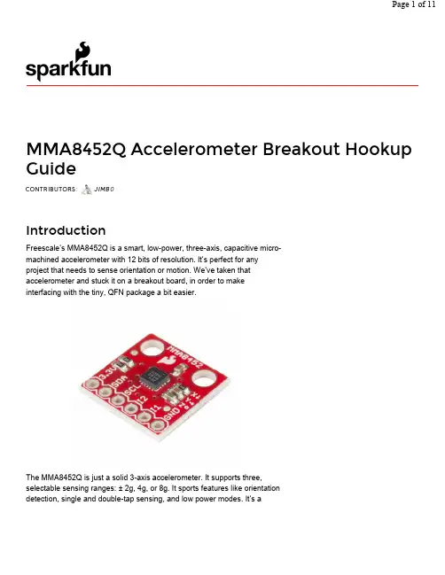
MMA8452Q Accelerometer Breakout Hookup GuideCONTRIBUTORS: JIMB0IntroductionFreescale’s MMA8452Q is a smart, low-power, three-axis, capacitive micro-machined accelerometer with 12 bits of resolution. It’s perfect for anyproject that needs to sense orientation or motion. We’ve taken thataccelerometer and stuck it on a breakout board, in order to makeinterfacing with the tiny, QFN package a bit easier.The MMA8452Q is just a solid 3-axis accelerometer. It supports three,selectable sensing ranges: ± 2g, 4g, or 8g. It sports features like orientationdetection, single and double-tap sensing, and low power modes. It’s adigital sensor – communicating over an I C interface –so you’ll get reliable, noise-free data using as few as two microcontroller pins to interact with the accelerometer.Covered In This TutorialThis tutorial aims to get you started up with the MMA8452Q as quickly as possible. It’s split into a handful of pages to explain how the board works and how to use it:•Hardware Overview –An overview of the MMA8452Q IC itself, and the breakout board we’ve stuffed it onto.•Example Hookup –How to connect the MMA8452Q to the ubiquitous Arduino. This hardware hookup is used in the next section…•Example Code –We’ve written an Arduino library to help make your Arduino sketch cleaner and easier to write. On this page we’ll show off an example sketch using the library and demonstrate how to use the library on your own to control the accelerometer.Required MaterialsTo follow along with this tutorial, the most unique components you’ll need are:•MMA8452Q Breakout Board –This is a good place to start (unless you plan on dead-bugging the tiny IC itself.•Arduino Board –You should be able to use any Arduino board you have handy – Arduino Uno, RedBoard, Pro, Mega, …anything.•330Ω Resistors –Assuming you’re using a 5V-based microcontroller, these will help protect the MMA8452Q from out-of-spec voltages hitting its pins.You’ll also need some sort of interconnect between the breakout and Arduino. A breadboard and jumper wires are always an easy combo.Finally, you’ll need to solder a connector onto the MMA8452Q breakout. If you’re using a breadboard to hook it up, we recommend straight male headers.Suggested ReadingBefore continuing on with this tutorial, we recommend you be somewhat familiar with the concepts in these tutorials:•Accelerometer Basics –This is a great primer on accelerometers –how they work, and why they’re used.•I C –An introduction to the communication protocol we’ll use to get our Arduino to talk to the MMA8452Q.22•Accelerometer Buying Guide –If you’re not sure whichaccelerometer is best for you, check out this guide.•Logic Levels –The MMA8452Q is a 3.3V device, so if you’re using a 5V microcontroller (like the Arduino) you’ll have to pay attention to the logic levels!Hardware OverviewThe MMA8452Q Breakout Board breaks out a select few of the mostimportant pins on the accelerometer.A little bit about each pin:Pin Label Pin FunctionInput/OutputNotes 3.3V Power SupplyInput Should be between 1.95 - 3.6V SDA I C Data Signal Bi-directional Bi-directional data line. Voltage should not exceed power supply (e.g. 3.3V).SCL I C ClockSignalInput Master-controlled clock signal. Voltage should not exceed power supply (e.g. 3.3V).I2Interrupt 2Output Programmable interrupt — can indicate data ready, orientation change, tap, andmore.I1Interrupt 1Output Programmable interrupt — can indicatedata ready, orientation change, tap, andmore.GND Ground Input0V/common voltage.22Voltage Supply RequirementsThe big alert here is that the MMA8452Q has a maximum voltage of 3.6V – that range applies to both the power supply and the I C pins. If you’re using the sensor in a 3.3V system you can plug it right in, but if you’re using it with a 5V device (like an Arduino Uno), some level-shifting is required between devices.Fortunately, you don’t need a lot of power to make the MMA8452Q work. In normal operating mode it can require anywhere between 7 and 165 µA.Address Select JumperThe MMA8452Q features a selectable I C address –just in case you’re running multiple MMA8452Qs on the same bus (or maybe you have an address conflict). To select the address, a pin on the accelerometer – “SA0” – can be tied to either power or ground.SA0 VoltageMMA8452Q I C Address0V 0x1C3.3V (VCC)0x1DThe breakout board includes a jumper, on the back side, to help tie this pinhigh or low.By default the jumper is open, which will pull the SA0 pin high (there’s a resistor on the top side of the board to help accomplish that task). If you close the jumper, by applying a small solder blob to connect both pads together, SA0 will be pulled to ground.For most use cases, where you’re only using one MMA8452Q, you can leave this jumper untouched. In that case the I C address will be 0x1D.2222Example HookupSolder SomethingBefore you can plug the breakout board into a breadboard, or connect it to anything, you’ll need to solder connectors or wires to the break-out pins. What, exactly, you solder into the board depends on how you’re going to use it.If you’re going to use the breakout board in a breadboard or similar0.1"-spaced perfboard, we recommend soldering straight male headers into the pins (there are also long headers if you need ‘em).If you’re going to mount the breakout into a tight enclosure, you may want to solder wires (stranded or solid-core) directly into the pins.Simple HookupWe’ll use Arduino to communicate with the MMA8452Q and interpret the data from the sensor. Since we’re using I C, all we need is two wires between the Arduino and accelerometer (aside from power and ground).Here’s the hookup:We simply have to supply the accelerometer with power (3.3V and GND), then hookup the SCL and SDA lines between devices. A couple of 330Ω resistors in series on each I C line will help to perform some simple level shifting. If you want more advanced level shifting…Level ShiftingSince the MMA8452Q’s maximum voltage is 3.6V, you’ll need to do some level shifting between your Arduino and accelerometer. Powering theaccelerometer off the Arduino’s 3.3V rail is a good start, but you’ll also need to add some protection on the SDA and SCL lines.22In the example hookup above, we used a pair of series resistors on the SDA and SCL lines. This version of “level shifting” works in a pinch, but, if you want a more reliable level-shifting setup, we recommend using a more robust level shifter between the boards.There are a handful of logic-level shifting boards available. For example, here’s a hookup using a Bi-Directional Logic Level Shifter between Arduino and accelerometer:Or, if you just want to skip level shifting entirely, you can use a 3.3V Arduino Pro(or Pro Mini), and run the whole system at 3.3V. As anyone who’s built electronics knows: there’s more than one way to skin the cat.Example CodeWe’ve written an Arduino library to make interfacing with the MMA8452Q as easy as can be. Click here to download the library. Or you can grab the latest, greatest version over on the GitHub repository.To install the library, extract the SFE_MMA8452Q folder into the libraries folder within your Arduino sketchbook. For help with Arduino library installations, we recommend checking out our How to Install an Arduino Library tutorial.Load Up the Example SketchOnce you’ve installed the SFE_MMA8452Q library, restart Arduino. Then go to File> Examples> SFE_MMA8452Q> MMA8452Q_Basic to open the example sketch.Once you’ve set your Board and Serial Port, upload the sketch to your Arduino. Then open the serial monitor. You’ll begin to see acceleration values stream by, in addition to some information about the sensor’s orientation.Try moving the sensor around to change those values. If it is motionless, flat on the desk, then an acceleration of 1g should be felt on the z-axis, while the others feel around 0. Test the other axes by rotating the board and making them feel the pull of gravity.Using the SFE_MMA8452Q LibraryHere are some tips on using the MMA8452Q Arduino library so you can embed it into an Arduino sketch of your own.Include the Library (Global)To begin, you need to “include” the library in your sketch:#include <Wire.h> // Must include Wire library for I2C#include <SFE_MMA8452Q.h> // Includes the SFE_MMA8452Q libraryThe library also requires that you include Wire.h in your sketch. Make sure you include that before you include the SFE_MMA8452Q.h file.Create an MMA8452Q Object (Global)Once the library is included, you can create an MMA8452Q object. This line of code will do it for you:MMA8452Q accel; // Default MMA8452Q object create. (Address =0x1D)Optionally, you can define the 7-bit I C address of your MMA8452Q in this2parameter, using one of these lines of code:MMA8452Q accel(0x1C); // Initialize the MMA8452Q with an I2C a ddress of 0x1C (SA0=0)MMA8452Q accel(0x1D); // Initialize the MMA8452Q with an I2C a ddress of 0x1D (SA0=1)But if you’ve left the address jumper untouched (meaning the “SA0” pin is connected to VCC), you can call the default (no parameter) constructor shown earlier.Initialize the MMA8452Q (Setup)Finally, in the setup()function of your sketch, you can initialize the accelerometer using the init()function. The init()function verifies communication with the accelerometer, and sets up the full-scale range and output data rate.Again, you have a few options here. You can use a simple declaration like below. This will initialize the accelerometer with range of ±2g and an output data rate of 800 Hz(turns the accelerometer up to the max!):accel.init(); // Default init: +/2g and 800Hz ODRIf you want to specify the acceleration and output data rate, you can instead use an init()function like this:accel.init([scale], [odr]); // Init and customize the FSR and ODRScale can be either SCALE_2G, SCALE_4G, or SCALE_8G. The “odr” variable can be either ODR_800, ODR_400, ODR_200, ODR_100, ODR_50, ODR_12, ODR_6, or ODR_1, respectively setting the data rate to 800, 400, 200, 100, 50, 12.5, 6.25, or 1.56 Hz.Reading and Using ValuesOnce you’ve set the accelerometer up, you can immediately start reading the data coming out of the chip. Reading and using the values is a two-step process. First, call the read()function to pull in the values.accel.read(); // Update acceleromter dataAfter you’ve called the read()function, you can use either of two sets of values to use the data. Reading from the x, y, and z class variables will return a signed 12-bit integer read straight out of the accelerometer.xAcceleration =accel.x; // Read in raw xaxis acceleration dataSerial.print("Acceleration on the xaxis is ");Serial.println(xAcceleration);Or, if you want a value with physical units, you can use the cx, cy, and cz class variables. These are the calculated acceleration values read out of the accelerometer; they’ll be in units of g’s.zAcceleration =accel.cz; // Read in calculated zaxis acceler ationSerial.print("Acceleration on the zaxis is: ");Serial.print(zAcceleration);Serial.println(" g's");Remember! Those variables are only updated after the read()function is called. Make sure that happens before you start using acceleration values.Reading Portrait/LandscapeThe MMA8452Q has all sorts of nifty, extra features, one of which is orientation detection–it can estimate if it’s being held in landscape mode, portrait mode, or flat.To read the portrait/landscape data from the accelerometer, use the readPL()function. This function returns a byte, which will either be equal to PORTRAIT_U, PORTRAIT_D, LANDSCAPE_R, LANDSCAPE_L, or LOCKOUT.byte pl =accel.readPL();switch(pl){case PORTRAIT_U:Serial.print("Portrait Up");break;case PORTRAIT_D:Serial.print("Portrait Down");break;case LANDSCAPE_R:Serial.print("Landscape Right");break;case LANDSCAPE_L:Serial.print("Landscape Left");break;case LOCKOUT:Serial.print("Flat");break;}As in the example above, you can use if or switch statements to check which orientation your accelerometer is in.Resources & Going FurtherThanks for reading! We’re excited to see what you build with theMMA8452Q. If you’re left needing more MMA8452Q-related documentation, check out some of these resources:•MMA8452Q Datasheet–Loads of information about theMMA8452Q’s electrical characteristics, registers, communicationspecifications, and more.•MMA8452Q Breakout Schematic–PDF schematic of theMMA8452Q Breakout board.•MMA8452Q Breakout Eagle Files–PCB design files for theMMA8452Q Breakout.•MMA8452Q Breakout GitHub Repo–Design files and example code all related to the MMA8452Q.Going FurtherIf you can’t already tell, we love accelerometers! Check out all of the tutorials and projects we’ve created that feature an accelerometer and more.•Are You Okay? Widget–Check out how Elecia embedded theMMA8452Q into a stuffed animal to create the Are-You-OK Widget.Are You Okay? Shake the stuffed animal to send a tweet and let yourbuddy know.•Getting Started with the RedBot –The MMA8452Q is used with the RedBot Kit to add bump detection.•Das Blinken Top Hat –Add an accelerometer to your LED-covered top hat, so you can control the blink pattern based on how your headis tilted.Das Blinken Top Hat! An accelerometer-controlled LED-covered dress hat.•Simon Tilts –Accelerometers aren’t the only sensors capable of sensing tilt. Check out the Simon Tilt game, which uses a really ingenious, optical method of detecting six different orientations.•Dungeons and Dragons Dice Gauntlet –You can embed anaccelerometer into your D&D bracers and roll virtual dice whenever you shake your arm!Page 11of 112/12/2015https:///tutorials/mma8452q-accelerometer-breakout-hookup-guide?_ga=1.151550015.72...。

飞思卡尔芯片飞思卡尔(Freescale)是一家拥有嵌入式半导体解决方案的全球领先制造商。
该公司的产品覆盖了自动驾驶汽车、智能手机、物联网以及工业自动化等领域。
飞思卡尔芯片是该公司的核心产品之一,下面将对其进行详细介绍。
飞思卡尔芯片是一种用于嵌入式系统的半导体芯片,具有高性能、低能耗的特点。
它可以运行复杂的应用程序,并提供丰富的外设接口,以满足各种设备的需求。
飞思卡尔芯片使用先进的制造工艺,具有较高的集成度和稳定性,同时还具有较低的功耗和散热性能。
飞思卡尔芯片提供了多种型号和系列,以满足不同应用场景的需求。
例如,i.MX系列是用于智能手机和平板电脑等移动设备的芯片,具有高性能、低功耗和丰富的多媒体功能。
QorIQ系列则是用于工业和网络设备的芯片,具有高性能、可靠性和安全性。
飞思卡尔芯片的应用范围非常广泛。
在汽车行业,它可以用于自动驾驶系统、车载娱乐系统和车身控制系统等。
在消费电子行业,它可以用于智能手机、平板电脑和智能家居设备等。
在工业自动化领域,它可以用于工业机器人、智能仓储系统和智能制造设备等。
与传统的微控制器相比,飞思卡尔芯片具有更强大的计算能力和更丰富的外设接口。
它可以支持更复杂的算法和应用程序,并且可以实现更高的系统集成度。
此外,飞思卡尔芯片还具有较低的功耗和散热性能,能够降低系统的能耗和散热压力。
飞思卡尔芯片还提供了丰富的软件和开发工具,以便开发人员快速开发和调试嵌入式系统。
它支持多种操作系统和开发环境,如Linux、Android和Microcontroller等。
同时,飞思卡尔芯片还提供了可靠的技术支持和培训,以帮助客户解决技术和应用问题。
总之,飞思卡尔芯片是一种用于嵌入式系统的半导体芯片,具有高性能、低能耗和丰富的外设接口。
它可以满足各种设备的需求,在多个行业具有广泛的应用前景。
随着物联网和智能制造技术的发展,飞思卡尔芯片将为各种智能设备的发展提供强大的支持。
飞思卡尔智能车电磁组分区算法介绍写在之前的话:1、⽬前我是⼀名在校学⽣,这也是我第⼀次写博客,不周之处,请多谅解;2、此算法并⾮原创,借鉴⾃⼭东德州学院第⼋届⽩杨队(PS:个⼈看法,对于⼀些⼈把别⼈的开源东西改头换⾯⼀下就说是⾃⼰的原创⾏为⼗分鄙视);3、对于此算法的理解和说明并⾮纸上谈兵,算法已经被我运⽤到了⼩车⽐赛中并取得好的成绩(具体就不多说了,⽐赛时车莫名其妙坏了,⽐赛前调试的速度绝对能进国赛,⽐较遗憾),总之这算法是我尝试过的最好的算法;4、这⼀次所介绍的只是路径算法和⼀些知识普及,后⾯有时间会介绍其余部分算法及许多好的思路(舵机电机控制思路(不只是简单的PID),双车策略);5、希望对于这⽅⾯有涉及的⼈能与我联系并交流或指出不⾜之处。
---------------------------------------------------------------分割线-----------------------------------------------------------------------------⼀、没有这⽅⾯了解的可以看看 飞思卡尔智能车分为三组:摄像头、光电、电磁,我做的是电磁车,三种车队区别在于传感器的不同,所以获得路径信息的⽅法也不⼀样,摄像头和光电识别的是赛道上的⿊线(⽩底赛道),⽽电磁车则是检测埋在赛道下的通⼊100mh电流的漆包线,摄像头和光电采⽤的是摄像头和ccd作为传感器,电磁则是⽤电感放在漆包线周围,则电感上就会产⽣感应电动势,且感应电动势的⼤⼩于通过线圈回路的磁通量成正⽐,⼜因为漆包线周围的磁感应强度不同,因此不同位置的电感的感应电动势就不同,因此就可以去确定电感位置;因此在车⼦前⾯设置了50cm的前瞻,电感布局如下(怎么发不了图⽚):分为两排,前排3个,编号0,1,2(前期还加了两个竖直电感⽤来帮助过直⾓弯,后来改为了⼋字电感);后排2个,编号3,4;现在车⼦获得了不同位置的感应电动势的⼤⼩了,但这些值是不能处理的:1、感应电动势太微弱;2、是模拟信号,信号太微弱就放⼤它;这就涉及到模拟电路的知识了,就不多说了(因为要把这讲完到PCB绘制的篇幅就⾜够写另开⼀号专门写这些⽅⾯来(PS:题外话(我的题外话⽐较多)):放⼤部分外围你设计的再好也抵不过⼀个更好的芯⽚,有两个例⼦,⼀个是我⾃⼰的:之前⽤的是NE5532,但是效果不理想,加了好多什么滤波,补偿,都⽤上,没⽤,软件⾥处理后⾯再说,后来⼀狠⼼换了AD620,感觉像是春天来了,因为它是仪⽤放⼤器,还有就是贵。

FREESCALE的三轴加速传感器设计方案
概述: 加速度传感器用于检测倾斜、运动、定位、振动和撞击力下产生的变化。
对那些需要以小型封装结构满足快速响应、高灵敏度、低电流消耗、低
电压操作和待机模式的消费电子客户来说飞思卡尔加速度传感器是理想的选
主要特性:
MMA7260QT 低成本微型电容式加速度传感器采用了信号调理、单极低通滤波器和温度补偿技术,并且提供4 个量程可选,用户可在4 个灵敏度中的选择。
该器件带有低通滤波并已做零g 补偿。
本产品还提供休眠模式,因而是电池充电的手持设备产品的理想之选。
特性
可选灵敏度(1.5g/2g/4g/6g)
低功耗:500 μA
休眠模式:3 μA
低压运行:2.2 V - 3.6 V
6mm x 6mm x 1.45 mm 的无引线四方扁平(QFN) 封装;
高灵敏度(800 mV/g @ 1.5g)
快速开启
低通滤波器具备内部信号调理
设计稳定、防震能力强
无铅焊接
环保封装
成本低
方案特性:。
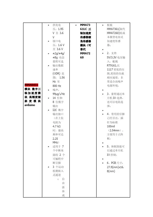
MMA8451模块数字三轴加速度模块高精度倾斜度模块arduino •供电电压:1.95V 至3.6V•接口电压:1.6 V至 3.6 V•±2g/±4g/±8g 动态量程可选•输出数据速率(ODR) 范围: 1.56Hz 至800 Hz•噪声:99μg/√Hz•14 位和8 位数字输出•I2C 数字输出接口(在上拉电阻为4.7 kΩ时,最高频率可达2.25MHz)•适用于7个中断来源的 2 个可编程中断引脚• 3 个运动检测嵌入式通道o自由落体或•MMA7361LC 三轴加速度传感器倾角传感器模块(可替代MMA7260•板载MMA7361(取代MMA7260)低成本微型电容式加速度传感器;••2、支持5V/3.3V电压输入,板载RT9161,比1117更低的压降,更快的负载相应速度,非常适合高噪声电源环境;••3、量程通过单片机IO选择,也可以电阻选择;••4、常用的引脚已经引出,插针为标准100mil(2.54mm),方便用于点阵板;••5、休眠使能可以通过单片机IO控制;••6、PCB尺寸:27.9(mm)x16.8(mm)。

飞思卡尔半导体公司推出新的微机电系统加速计用于智能电表应用的物理篡改防护
飞思卡尔半导体公司(NYSE:FSL)日前推出新的微机电系统(MEMS)加速计,提供超低功耗和简单的即插即用方法来进行倾斜阈值检测,用于智能电表应用的物理篡改防护。
飞思卡尔的Xtrinsic MMA8491Q 节能高效加速计将产品组合扩展至工业市场,该市场需要宽引脚间距、可以目测检查的引线和较长的产品生命周期。
飞思卡尔副总裁兼传感器与致动器解决方案事业部总经理Seyed Paransun 表示:智能电表的数量随着互联家居和电网的出现而激增,物理篡改防护是一个关键要求。
飞思卡尔通过简单易用、经济高效、功耗极低且具有特定嵌入式功能的 3 轴加速计满足了这个需求。
Xtrinsic MMA8491Q 加速计专为需要降低复杂性并具备高级系统集成的应用而设计,其倾斜阈值传感在检测物理篡改的飞思卡尔系统级智能电表参考设计中起着不可或缺的作用(在Sensor Expo 2012 和Metering Europe 2012 中推出)。
通过倾斜角的变化检测电表的运动,并在发生篡改事件时通知市政公司。
Xtrinsic MMA8491Q 加速计的设计非常灵活,可用于智能电表以外的、。

MMA7455加速度传感器使⽤MMA7455加速度传感器是freescale公司的看下⾯的链接这个页⾯可以下载它的datasheet,和应⽤笔记,很重要,⾥⾯还有⼀些参考例程。
简单说⼀下这个传感器的,是3轴加速度传感器。
数字输出接⼝是IIC或者SPI,很容易使⽤单⽚机控制该芯⽚,它还有低功耗模式,可以⽤于电池供电。
检测最⼤加速度是正负8g,有不同的灵敏度,如16/g,32/g,64/g,可以选择的,使⽤这个芯⽚最主要还是对芯⽚的寄存器的操作,我具体说⼀下地址为06-08的寄存器保存的就是XYZ轴的加速度数值,可以同过IIC读出来,然后利⽤灵敏度转化为实际的加速度数值。
那个DRDY是数值转换完成状态位,在读取数值前,要检测该位,只有它为1的时候,说明数据转换完成,可以读取。
因为这个芯⽚是利⽤变化的电容来检测加速度的,所以有个初始值的误差,需要校正,校正寄存器是下图,就是说,上⾯的06-08寄存器的值,是加上这个校正值后的值,注意这个校正寄存器可以保存正负校正值,都是⽤⼆进制补码格式的,啥是⼆进制补码,可以去google,不多说了。
不过这⾥说明⼀下这个校正值的权值是1/2灵敏度,就是说如果X值是5,你要给它归零,你就需要在X校正寄存器写⼊-5*2,也就是-10,-10的⼆进制补码是1111 0110 这是8位⼆进制的值,要是16位⼆进制的值就是1111 1111 1111 0110,就是0xFFF6,我们就要把0xFFF6写⼊10,11寄存器⾥⾯,那个是⾼低位就不⽤说了吧。
下⾯的图⽚是从它的应⽤技术⽂档⾥⾯截取的。
这个芯⽚有⼏种运⾏模式,省电模式,测量模式,⽔平检测模式,脉冲检测模式,我们使⽤测量模式。
主要的流程也就是这么多了。
下⾯对照程序说明⼀下流程这样⽐较直观。
ISendStr(0x3a,0x16,0x09,1);是配置⼯作模式,测量模式,正负4G,ISendStr(0x1D<<1,0x10,6,1);ISendStr(0x1D<<1,0x11,0,1);ISendStr(0x1D<<1,0x12,17,1);ISendStr(0x1D<<1,0x13,0,1);ISendStr(0x1D<<1,0x14,0xfd,1);ISendStr(0x1D<<1,0x15,0xff,1);添加校正值,要经过测试,⾃⼰选择⽐较合适的值。
MMA8452模块,高精度倾斜传感器模块模块型号:GY-45-52供电电源:3-5v(通信完全兼容5v工作系统)模块尺寸长*宽=14.5mm * 20.5 mm安装孔直径3mm ,孔距15mm提供51测试代码提供文档MMA8452Q: 3 轴12 位/8位数字加速度传感器AN4076:MMA8451、2、3Q 的数据操作与基本设置AN4068:使用MMA8451、2、3Q 实现嵌入式方向检测AN4069:MMA8451、2、3Q 的偏移校准AN4070: 使用MMA8451、2、3Q 实现动作和自由落体检测AN4073: 利用MMA8451Q 中的32 采样先进先出(FIFO)缓存AN4077: MMA845xQ 设计检查表和线路板贴装安装指南AN4076SW:AN4076 示例代码,附AN4076 应用笔记MMA8452Q 是一款具有12位分辨率的智能低功耗、三轴、电容式微机械加速度传感器。
这款加速度传感器具有丰富嵌入式功能,带有灵活的用户可编程选项,可以配置多达两个中断引脚。
嵌入式中断功能可以节省整体功耗,解除主处理器不断轮询数据的负担。
MMA8452Q 具有±2g/±4g/±8g的用户可选量程,可以实时输出高通滤波数据和非滤波数据。
该器件可被配置成利用任意组合可配置嵌入式的功能生成惯性唤醒中断信号,这就使MMA8452Q 在监控事件同时,在静止状态保持低功耗模式。
特性供电电压:1.95 V 至3.6 V接口电压:1.6 V 至3.6 V±2g/±4g/±8g 动态量程可选输出数据速率(ODR) 范围:1.56 Hz 至800 Hz噪声:99μg/√Hz12位和8位数字输出I2C 数字输出接口(在上拉电阻为4.7 kΩ时,最高频率可达2.25 MHz)适用于6个中断来源的2个可编程中断引脚3 个运动检测嵌入式通道自由落体或运动检测:1通道–脉冲检测:1通道–晃动检测:1通道带有设定滞后补偿的方向(横向/纵向)检测自动唤醒和自动休眠的ODR可自动更改高通滤波数据可实时输出自检测符合RoHS 标准功耗:6 μA – 165 μA典型应用电子罗盘应用静止方向检测(横向/纵向、上/下、左/右、前/后位置识别)笔记本、电子书阅读器和便携式电脑跌落和自由落体检测实时方向检测(虚拟现实和游戏机3D 用户位置反馈)实时活动分析(步程计步进计数、用于HDD 的自由坠落检测、推测航行法GPS 备份)适用于便携式节能产品的动作检测(用于手机、PDA、GPS、游戏机的自动睡眠和自动唤醒)冲击和振动检测(机电一体化补偿、装运和保修使用记录)用户界面(通过方向更改实现菜单滚动、用于按钮替换的标签检测)。
飞思卡尔飞思卡尔单片机快速上手指南单片机快速上手指南飞思卡尔飞思卡尔半导体半导体IMM FAE 团队2014年9月 · 审阅稿飞思卡尔半导体是全球领先的单片机供应商,其单片机产品包含多种内核,有数百个系列。
为支持用户使用这些产品,飞思卡尔提供了丰富的网站资源、文档及软硬件工具,另外,我们还有众多的第三方合作伙伴及公共平台的支持。
对于不熟悉飞思卡尔产品和网站的初学者来说,了解和使用这些资源这无疑是一个令人望而生畏的浩瀚工程。
本指南的目的,就是给初学者提供一个指导,让他们不被这些海量信息淹没;用户根据本指导提供的操作步骤,能迅速找到所需的资源,了解如何使用相关的工具。
在本指南中,我们以飞思卡尔的新一代Kinetis 单片机K22系列为例,介绍了如何获取与之相关的资源,如何对其进行软硬件设计和开发。
实际上,这些方法也适用于其它的单片机系列。
当然,对于其它有较多不同之处的产品,我们也会继续推出相应的文档,供广大用户参考。
目录第一章. 如何获取技术资料与支持 第二章. 如何如何选择选择选择产品产品产品、、申请样片及购买申请样片及购买少量少量少量芯片芯片芯片和和开发工具 第三章. 飞思卡尔飞思卡尔单片机的开发环境单片机的开发环境单片机的开发环境、、开发工具开发工具和生态系统和生态系统 第四章. 如何如何阅读飞思卡尔的技术文档阅读飞思卡尔的技术文档 第五章. 飞思卡尔飞思卡尔单片机硬件设计指南单片机硬件设计指南 第六章. 飞思卡尔飞思卡尔单片机单片机单片机软软件开发开发指南指南第一章第一章 如何如何获取技术资料与支持获取技术资料与支持1.1 概述当用户使用飞思卡尔单片机芯片时,如何获取芯片的数据手册(Datasheet )、参考设计(Reference Manual )和官方例程等资源呢?另外当用户遇到了技术问题该如何获得帮助和解答呢?这里以Kinetis 的K22系列芯片为例为大家介绍如何解决这些问题。
Freescale Semiconductor Document Number: MMA8452QData Sheet: Technical DataRev. 5, 07/2012An Energy-Efficient Solution by Freescale© 2012 Freescale Semiconductor, Inc. All rights reserved.3-Axis, 12-bit/8-bitDigital AccelerometerThe MMA8452Q is a smart low-power, three-axis, capacitive micromachined accelerometer with 12 bits of resolution. This accelerometer is packed withembedded functions with flexible user programmable options, configurable to two interrupt pins. Embedded interrupt functions allow for overall power savings relieving the host processor from continuously polling data.The MMA8452Q has user selectable full scales of ±2g/±4g/±8g with high-pass filter filtered data as well as non-filtered data available real-time. The device can be configured to generate inertial wakeup interrupt signals from any combination of the configurable embedded functions allowing the MMA8452Q to monitor events and remain in a low power mode during periods of inactivity . The MMA8452Q is available in a 3 mm by 3 mm by 1 mm QFN package. Features • 1.95V to 3.6V supply voltage • 1.6V to 3.6V interface voltage•±2g/±4g/±8g dynamically selectable full-scale •Output Data Rates (ODR) from 1.56 Hz to 800 Hz •99 μg/√Hz noise•12-bit and 8-bit digital output •I 2C digital output interface•Two programmable interrupt pins for six interrupt sources •Three embedded channels of motion detection— Freefall or Motion Detection: 1 channel — Pulse Detection: 1 channel — Transient Detection: 1 channel–Orientation (Portrait/Landscape) detection with set hysteresis –Automatic ODR change for Auto-WAKE and return to SLEEP –High-Pass Filter Data available real-time –Self-T est–RoHS compliant–Current Consumption: 6 μA – 165 μATypical Applications •eCompass applications •Static orientation detection (Portrait/Landscape, Up/Down, Left/Right, Back/Front position identification)•Notebook, eReader and Laptop Tumble and Freefall Detection •Real-time orientation detection (virtual reality and gaming 3D user position feedback)•Real-time activity analysis (pedometer step counting, freefall drop detection for HDD, dead-reckoning GPS backup)•Motion detection for portable product power saving (Auto-SLEEP and Auto-WAKE for cell phone, PDA, GPS, gaming)•Shock and vibration monitoring (mechatronic compensation, shipping and warranty usage logging)•User interface (menu scrolling by orientation change, pulse detection for button replacement)ORDERING INFORMATIONPart NumberTemperature Range Package DescriptionShipping MMA8452QT -40°C to +85°C QFN-16Tray MMA8452QR1-40°C to +85°CQFN-16Tape and Reel MMA8452Q16 PIN QFN3 mm by 3 mm by 1 mmCASE 2077-02Top and Bottom ViewTop ViewPin Connections12345910111213141516876N C V D D N C VDDIO BYP NC SCL GNDNC GND INT1GND INT2S A 0N CS D AContents1Block Diagram and Pin Description . . . . . . . . . . . . . . . . . . . . . . . . . . . . . . . . . . . . . . . . . . . . . . . . . . . . . . . . . . . . . . . . . 31.1Soldering Information . . . . . . . . . . . . . . . . . . . . . . . . . . . . . . . . . . . . . . . . . . . . . . . . . . . . . . . . . . . . . . . . . . . . . . . . . 5 2Mechanical and Electrical Specifications. . . . . . . . . . . . . . . . . . . . . . . . . . . . . . . . . . . . . . . . . . . . . . . . . . . . . . . . . . . . . 62.1Mechanical Characteristics. . . . . . . . . . . . . . . . . . . . . . . . . . . . . . . . . . . . . . . . . . . . . . . . . . . . . . . . . . . . . . . . . . . . . 62.2Electrical Characteristics. . . . . . . . . . . . . . . . . . . . . . . . . . . . . . . . . . . . . . . . . . . . . . . . . . . . . . . . . . . . . . . . . . . . . . . 72.3I2C Interface Characteristics. . . . . . . . . . . . . . . . . . . . . . . . . . . . . . . . . . . . . . . . . . . . . . . . . . . . . . . . . . . . . . . . . . . . 82.4Absolute Maximum Ratings . . . . . . . . . . . . . . . . . . . . . . . . . . . . . . . . . . . . . . . . . . . . . . . . . . . . . . . . . . . . . . . . . . . . 9 3Terminology . . . . . . . . . . . . . . . . . . . . . . . . . . . . . . . . . . . . . . . . . . . . . . . . . . . . . . . . . . . . . . . . . . . . . . . . . . . . . . . . . . . 103.1Sensitivity . . . . . . . . . . . . . . . . . . . . . . . . . . . . . . . . . . . . . . . . . . . . . . . . . . . . . . . . . . . . . . . . . . . . . . . . . . . . . . . . . 103.2Zero-g Offset. . . . . . . . . . . . . . . . . . . . . . . . . . . . . . . . . . . . . . . . . . . . . . . . . . . . . . . . . . . . . . . . . . . . . . . . . . . . . . . 103.3Self-Test . . . . . . . . . . . . . . . . . . . . . . . . . . . . . . . . . . . . . . . . . . . . . . . . . . . . . . . . . . . . . . . . . . . . . . . . . . . . . . . . . . 10 4Modes of Operation . . . . . . . . . . . . . . . . . . . . . . . . . . . . . . . . . . . . . . . . . . . . . . . . . . . . . . . . . . . . . . . . . . . . . . . . . . . . . 10 5Functionality . . . . . . . . . . . . . . . . . . . . . . . . . . . . . . . . . . . . . . . . . . . . . . . . . . . . . . . . . . . . . . . . . . . . . . . . . . . . . . . . . . . 115.1Device Calibration. . . . . . . . . . . . . . . . . . . . . . . . . . . . . . . . . . . . . . . . . . . . . . . . . . . . . . . . . . . . . . . . . . . . . . . . . . . 125.28-bit or 12-bit Data . . . . . . . . . . . . . . . . . . . . . . . . . . . . . . . . . . . . . . . . . . . . . . . . . . . . . . . . . . . . . . . . . . . . . . . . . . 125.3Low-Power Modes vs. High-Resolution Modes . . . . . . . . . . . . . . . . . . . . . . . . . . . . . . . . . . . . . . . . . . . . . . . . . . . . 125.4Auto-WAKE/SLEEP Mode . . . . . . . . . . . . . . . . . . . . . . . . . . . . . . . . . . . . . . . . . . . . . . . . . . . . . . . . . . . . . . . . . . . . 125.5Freefall and Motion Detection. . . . . . . . . . . . . . . . . . . . . . . . . . . . . . . . . . . . . . . . . . . . . . . . . . . . . . . . . . . . . . . . . . 125.6Transient Detection. . . . . . . . . . . . . . . . . . . . . . . . . . . . . . . . . . . . . . . . . . . . . . . . . . . . . . . . . . . . . . . . . . . . . . . . . . 135.7Pulse Detection. . . . . . . . . . . . . . . . . . . . . . . . . . . . . . . . . . . . . . . . . . . . . . . . . . . . . . . . . . . . . . . . . . . . . . . . . . . . . 135.8Orientation Detection . . . . . . . . . . . . . . . . . . . . . . . . . . . . . . . . . . . . . . . . . . . . . . . . . . . . . . . . . . . . . . . . . . . . . . . . 135.9Interrupt Register Configurations . . . . . . . . . . . . . . . . . . . . . . . . . . . . . . . . . . . . . . . . . . . . . . . . . . . . . . . . . . . . . . . 155.10Serial I2C Interface . . . . . . . . . . . . . . . . . . . . . . . . . . . . . . . . . . . . . . . . . . . . . . . . . . . . . . . . . . . . . . . . . . . . . . . . . . 15 6Register Descriptions. . . . . . . . . . . . . . . . . . . . . . . . . . . . . . . . . . . . . . . . . . . . . . . . . . . . . . . . . . . . . . . . . . . . . . . . . . . . 186.1Data Registers . . . . . . . . . . . . . . . . . . . . . . . . . . . . . . . . . . . . . . . . . . . . . . . . . . . . . . . . . . . . . . . . . . . . . . . . . . . . . 196.2Portrait/ Landscape Embedded Function Registers. . . . . . . . . . . . . . . . . . . . . . . . . . . . . . . . . . . . . . . . . . . . . . . . . 236.3Motion and Freefall Embedded Function Registers . . . . . . . . . . . . . . . . . . . . . . . . . . . . . . . . . . . . . . . . . . . . . . . . . 256.4Transient (HPF) Acceleration Detection. . . . . . . . . . . . . . . . . . . . . . . . . . . . . . . . . . . . . . . . . . . . . . . . . . . . . . . . . . 306.5Single, Double and Directional Pulse-Detection Registers. . . . . . . . . . . . . . . . . . . . . . . . . . . . . . . . . . . . . . . . . . . . 326.6Auto-WAKE/SLEEP Detection . . . . . . . . . . . . . . . . . . . . . . . . . . . . . . . . . . . . . . . . . . . . . . . . . . . . . . . . . . . . . . . . . 366.7Control Registers . . . . . . . . . . . . . . . . . . . . . . . . . . . . . . . . . . . . . . . . . . . . . . . . . . . . . . . . . . . . . . . . . . . . . . . . . . . 376.8User Offset Correction Registers . . . . . . . . . . . . . . . . . . . . . . . . . . . . . . . . . . . . . . . . . . . . . . . . . . . . . . . . . . . . . . . 40Related DocumentationThe MMA8452Q device features and operations are described in a variety of reference manuals, user guides, and application notes. To find the most-current versions of these documents:1.Go to the Freescale homepage at:/2.In the Keyword search box at the top of the page, enter the device number MMA8452Q.3.In the Refine Your Result pane on the left, click on the Documentation link.MMA8452QSensorsMMA8452QSensors1Block Diagram and Pin DescriptionFigure 1. Block DiagramFigure 2. Direction of the Detectable AccelerationsSDA SCLAuto-WAKE/SLEEPACTIVE ModeSLEEPMODE Options Low PowerLow Noise + Power High Resolution NormalMODE Options Low PowerLow Noise + Power High Resolution NormalACTIVE ModeWAKEMMA8452Q SensorsFigure 3 shows the device configuration in the six different orientation modes. These orientations are defined as the following: PU = Portrait Up, LR = Landscape Right, PD = Portrait Down, LL = Landscape Left, BACK and FRONT side views. There are several registers to configure the orientation detection and are described in detail in the register setting section.Figure 3. Landscape/Portrait OrientationTop ViewPUEarth GravityPin 1Xout @ 0g Yout @ -1g Zout @ 0gXout @ 1g Yout @ 0g Zout @ 0gXout @ 0g Yout @ 1g Zout @ 0gXout @ -1g Yout @ 0g Zout @ 0gLLPDLRSide ViewFRONTXout @ 0g Yout @ 0g Zout @ 1gBACKXout @ 0g Yout @ 0g Zout @ -1gTable1. Pin DescriptionsPin #Pin Name Description Pin Status1VDDIO Power Supply for IO pins (1.62V - 3.6V)Input2BYP Bypass capacitor (0.1 μF)Input3NC Leave open. Do not connect.Open4SCL I2C Serial Clock Open Drain5GND Connect to Ground Input6SDA I2C Serial Data Open Drain7SA0I2C Least Significant Bit of the Device I2C Address Input8NC Internally not connected (can be GND or VDD)Input9INT2Inertial Interrupt 2Output10GND Connect to Ground Input11INT1Inertial Interrupt 1Output12GND Connect to Ground Input13NC Internally not connected (can be GND or VDD)Input14VDD Internal Power Supply (1.95V - 3.6V)Input15NC Internally not connected (can be GND or VDD)Input16NC Internally not connected (can be GND or VDD)Input The device power is supplied through VDD line. Power supply decoupling capacitors (100 nF ceramic plus 4.7 µF bulk, or a single 4.7 µF ceramic) should be placed as near as possible to the pins 1 and 14 of the device.The control signals SCL, SDA, and SA0 are not tolerant of voltages more than VDDIO + 0.3V. If VDDIO is removed, the control signals SCL, SDA, and SA0 will clamp any logic signals with their internal ESD protection diodes.The functions, the threshold and the timing of the two interrupt pins (INT1 and INT2) are user programmable through the I2C interface. The SDA and SCL I2C connections are open drain and therefore require a pullup resistor as shown in the application diagram in Figure 4.1.1Soldering InformationThe QFN package is compliant with the RoHS standard. Please refer to AN4077.MMA8452Q SensorsMMA8452Q Sensors2Mechanical and Electrical Specifications2.1Mechanical CharacteristicsTable 2. Mechanical Characteristics @ VDD = 2.5V, VDDIO = 1.8V, T = 25°C unless otherwise noted .ParameterTest Conditions SymbolMinTyp MaxUnitMeasurement Range (1)1.Dynamic Range is limited to 4g when the Low-Noise bit in Register 0x2A, bit 2 is set.FS[1:0] set to 002g ModeFS±2gFS[1:0] set to 014g Mode ±4FS[1:0] set to 108g Mode ±8SensitivityFS[1:0] set to 002g ModeSo1024counts/g FS[1:0] set to 014g Mode 512FS[1:0] set to 108g Mode256Sensitivity Accuracy (2)2.Sensitivity remains in spec as stated, but changing Oversampling mode to Low Power causes 3% sensitivity shift. This behavior is also seen when changing from 800 Hz to any other data rate in the Normal, Low Noise + Low Power or High Resolution mode.Soa±2.64%Sensitivity Change vs. TemperatureFS[1:0] set to 002g ModeTCSo ±0.008%/°CFS[1:0] set to 014g Mode FS[1:0] set to 108g ModeZero-g Level Offset Accuracy (3)3.Before board mount.FS[1:0] 2g, 4g, 8g TyOff ±17 mg Zero-g Level Offset Accuracy Post Board Mount (4)4.Post Board Mount Offset Specifications are based on an 8 Layer PCB, relative to 25°C.FS[1:0] 2g, 4g, 8g TyOffPBM ±20 mg Zero-g Level Change vs. Temperature -40°C to 85°CTCOff±0.15mg/°CSelf-Test Output Change (5)X Y Z5.Self-Test is one direction only.FS[1:0] set to 0 4g ModeVst+181+255+1680LSBODR Accuracy 2 MHz Clock±2%Output Data Bandwidth BWODR/3ODR/2Hz Output NoiseNormal Mode ODR = 400 Hz Noise 126 µg/√Hz Output Noise Low-Noise Mode (1)Normal Mode ODR = 400 HzNoise 99µg/√Hz Operating Temperature RangeTop-40+85 °CMMA8452QSensors2.2Electrical CharacteristicsTable 3. Electrical Characteristics @ VDD = 2.5V, VDDIO = 1.8V, T = 25°C unless otherwise noted .ParameterTest ConditionsSymbol Min Typ Max Unit Supply VoltageVDD (1)1.There is no requirement for power supply sequencing. The VDDIO input voltage can be higher than the VDD input voltage.1.952.53.6 V Interface Supply VoltageVDDIO (1)1.621.8 3.6VLow-Power ModeODR = 1.56 Hz I dd LP6μAODR = 6.25 Hz 6ODR = 12.5 Hz 6ODR = 50 Hz 14ODR = 100 Hz 24ODR = 200 Hz 44ODR = 400 Hz 85ODR = 800 Hz 165Normal ModeODR = 1.56 Hz I dd24μA ODR = 6.25 Hz 24ODR = 12.5 Hz 24ODR = 50 Hz 24ODR = 100 Hz 44ODR = 200 Hz 85ODR = 400 Hz 165ODR = 800 Hz165Current during Boot Sequence, 0.5 mSec max duration using recommended Bypass Cap VDD = 2.5V Idd Boot 1mA Value of Capacitor on BYP Pin -40°C 85°CCap 75100470 nF STANDBY Mode Current @25°C VDD = 2.5V, VDDIO = 1.8VSTANDBY ModeI dd Stby1.85μA Digital High Level Input Voltage SCL, SDA, SA0VIH 0.7*VDDIOV Digital Low-Level Input Voltage SCL, SDA, SA0VIL0.3*VDDIOV High Level Output Voltage INT1, INT2I O = 500 μA VOH 0.9*VDDIOV Low-Level Output Voltage INT1, INT2I O = 500 μA VOL 0.1*VDDIO V Low-Level Output Voltage SDAI O = 500 μAVOLS0.1*VDDIOV Power on Ramp Time0.0011000ms Time from VDDIO on and VDD > Vmin until I 2C ready for operation Cbyp = 100 nF BT —350500 µs Turn-on time (STANDBY)(2)2.Note that the first sample is typically not very precise. Depending on ODR/MODS settings, a minimum of three samples is recommended for full precision.Ton Stby 1.1/ODRs Turn-on time (Power Down to STANDBY)Ton 2ms Operating Temperature RangeTop-40+85°CMMA8452Q Sensors2.3I 2C Interface CharacteristicsTable 4. I 2C Slave Timing Values (1)1.All values referred to VIH (min) and VIL (max) levels.ParameterSymbolI 2C Fast Mode UnitMin Max SCL Clock FrequencyPullup = 4.7 k Ω, Cb = 20 pF Pullup = 4.7 k Ω, Cb = 40 pF Pullup = 4.7 k Ω, Cb = 400 pF Pullup = 1 k Ω, Cb = 20 pF Pullup = 1 k Ω, Cb = 400 pFf SCL00000 2.250100Nonfunctional4.50750MHz kHz —MHz kHz Bus Free Time between STOP and START Condition t BUF 1.3μs Repeated START Hold Time t HD;STA 0.6μs Repeated START Setup Time t SU;STA 0.6μs STOP Condition Setup Time t SU;STO 0.6μs SDA Data Hold Time (2)2.t HD;DAT is the data hold time that is measured from the falling edge of SCL, applies to data in transmission and the acknowledge.t HD;DAT 0.05(3)3.The maximum t HD;DAT could be 3.45 μs and 0.9 μs for Standard mode and Fast mode, but must be less than the maximum of t VD;DAT or t VD;ACK by a transition time.μs SDA Valid Time (4)4.t VD;DAT = time for Data signal from SCL LOW to SDA output (HIGH or LOW, depending on which one is worse).t VD;DAT 0.9(3)μs SDA Valid Acknowledge Time (5)5.t VD;ACK = time for Acknowledgement signal from SCL LOW to SDA output (HIGH or LOW, depending on which one is worse).t VD;ACK 0.9(3)μs SDA Setup Time t SU;DAT 100(6)6.A Fast mode I 2C device can be used in a Standard mode I 2C system, but the requirement t SU;DAT 250 ns must then be met. This willautomatically be the case if the device does not stretch the LOW period of the SCL signal. If such a device does stretch the LOW period of the SCL signal, it must output the next data bit to the SDA line t r (max) + t SU;DAT = 1000 + 250 = 1250 ns (according to the Standard mode I 2C specification) before the SCL line is released. Also the acknowledge timing must meet this setup time ns SCL Clock Low Time t LOW 4.7μs SCL Clock High Time t HIGH 4μsSDA and SCL Rise Time t r 1000ns SDA and SCL Fall Time (7) (8)7.Cb = total capacitance of one bus line in pF.8.The maximum t f for the SDA and SCL bus lines is specified at 300 ns. The maximum fall time for the SDA output stage t f is specified at 250ns. This allows series protection resistors to be connected in between the SDA and the SCL pins and the SDA/SCL bus lines without exceeding the maximum specified t f .t f 300ns Pulse width of spikes on SDA and SCL that must be suppressed by input filtert SP50nsMMA8452QSensorsFigure 5. I 2C Slave Timing Diagram2.4Absolute Maximum RatingsStresses above those listed as “absolute maximum ratings” may cause permanent damage to the device. Exposure to maximum rating conditions for extended periods may affect device reliability.Table 5. Maximum RatingsRatingSymbol Value Unit Maximum Acceleration (all axes, 100 μs)g max 5,000g Supply VoltageVDD -0.3 to + 3.6V Input voltage on any control pin (SA0, SCL, SDA)Vin -0.3 to VDDIO + 0.3V Drop TestD drop 1.8m Operating Temperature Range T OP -40 to +85°C Storage Temperature RangeT STG-40 to +125°CTable6. ESD and Latchup Protection CharacteristicsRatingSymbol Value Unit Human Body Model HBM ±2000V Machine Model MM ±200V Charge Device Model CDM ±500V Latchup Current at T = 85°C—±100mAThis device is sensitive to mechanical shock. Improper handling can cause permanent damage of the part or cause the part to otherwise fail.This device is sensitive to ESD, improper handling can cause permanent damage to the part.MMA8452Q Sensors3Terminology3.1SensitivityThe sensitivity is represented in counts/g. In 2g mode the sensitivity is 1024 counts/g. In 4g mode the sensitivity is 512 counts/g and in 8g mode the sensitivity is 256 counts/g.3.2Zero-g OffsetZero-g Offset (TyOff) describes the deviation of an actual output signal from the ideal output signal if the sensor is stationary. A sensor stationary on a horizontal surface will measure 0g in X-axis and 0g in Y -axis whereas the Z-axis will measure 1g. The output is ideally in the middle of the dynamic range of the sensor (content of OUT Registers 0x00, data expressed as 2's complement number). A deviation from ideal value in this case is called Zero-g offset. Offset is to some extent a result of stress on the MEMS sensor and therefore the offset can slightly change after mounting the sensor onto a printed circuit board or exposing it to extensive mechanical stress.3.3Self-TestSelf-T est checks the transducer functionality without external mechanical stimulus. When Self-T est is activated, an electrostatic actuation force is applied to the sensor, simulating a small acceleration. In this case the sensor outputs will exhibit a change in their DC levels which are related to the selected full scale through the device sensitivity . When Self-T est is activated, the device output level is given by the algebraic sum of the signals produced by the acceleration acting on the sensor and by the electrostatic test-force.4Modes of OperationFigure 6. MMA8452Q Mode Transition DiagramAll register contents are preserved when transitioning from ACTIVE to STANDBY mode. Some registers are reset when transitioning from STANDBY to ACTIVE. These are all noted in the device memory map register table. The SLEEP and WAKE modes are ACTIVE modes. For more information on how to use the SLEEP and WAKE modes and how to transition between these modes please refer to the functionality section of this document.Table 7. Mode of Operation DescriptionMode I 2C Bus State VDD VDDIOFunction DescriptionOFFPowered Down<1.8VVDDIO Can be > VDD The device is powered off. All analog and digital blocks are shutdown. I 2C bus inhibited.STANDBY I 2C communication with MMA8452Q is possible ONVDDIO = High VDD = HighACTIVE bit is cleared Only digital blocks are enabled.Analog subsystem is disabled. Internal clocks disabled.ACTIVE (WAKE/SLEEP)I 2C communication with MMA8452Q is possibleON VDDIO = High VDD = HighACTIVE bit is setAll blocks are enabled (digital, analog).SLEEPWAKESTANDBYOFFACTIVE5FunctionalityThe MMA8452Q is a low-power, digital output 3-axis linear accelerometer with a I2C interface and embedded logic used to detect events and notify an external microprocessor over interrupt lines. The functionality includes the following:•8-bit or 12-bit data which includes High-Pass Filtered data• 4 different oversampling options for compromising between resolution and current consumption based on application requirements•Additional Low-Noise mode that functions independently of the Oversampling modes for higher resolution•Low-Power and Auto-WAKE/SLEEP for conservation of current consumption•Single-/Double-pulse with directional information 1 channel•Motion detection with directional information or Freefall 1 channel•Transient detection based on a high-pass filter and settable threshold for detecting the change in acceleration above a threshold with directional information 1 channel•Portrait/Landscape detection with trip points fixed at 30° and 60° for smooth transitions between orientations.All functionality is available in 2g, 4g or 8g dynamic ranges. There are many configuration settings for enabling all the different functions. Separate application notes have been provided to help configure the device for each embedded functionality.Table8. Features of the MMA845xQ devicesFeature List MMA8451MMA8452MMA8453 Digital Resolution (Bits)141210 Digital Sensitivity (Counts/g)40961024256Data-Ready Interrupt Yes Yes Yes Single-Pulse Interrupt Yes Yes Yes Double-Pulse Interrupt Yes Yes Yes Directional-Pulse Interrupt Yes Yes YesAuto-WAKE Yes Yes YesAuto-SLEEP Yes Yes Yes Freefall Interrupt Yes Yes Yes32 Level FIFO Yes No NoHigh-Pass Filter Yes Yes YesLow-Pass Filter Yes Yes Yes Orientation Detection Portrait/Landscape = 30°, Landscape to Portrait = 60°,Yes Yes Yesand Fixed 45° ThresholdProgrammable Orientation Detection Yes No No Motion Interrupt with Direction Yes Yes Yes Transient Detection with High-Pass Filter Yes Yes YesLow-Power Mode Yes Yes Yes5.1Device CalibrationThe device interface is factory calibrated for sensitivity and Zero-g offset for each axis. The trim values are stored in Non Volatile Memory (NVM). On power-up, the trim parameters are read from NVM and applied to the circuitry. In normal use, further calibration in the end application is not necessary. However, the MMA8452Q allows the user to adjust the Zero-g offset for each axis after power-up, changing the default offset values. The user offset adjustments are stored in 6 volatile registers. For more information on device calibration, refer to Freescale application note, AN4069.5.28-bit or 12-bit DataThe measured acceleration data is stored in the OUT_X_MSB, OUT_X_LSB, OUT_Y_MSB, OUT_Y_LSB, OUT_Z_MSB, and OUT_Z_LSB registers as 2’s complement 12-bit numbers. The most significant 8-bits of each axis are stored in OUT_X (Y,Z)_MSB,so applications needing only 8-bit results can use these 3 registers and ignore OUT_X,Y, Z_LSB. To do this, theF_READ bit in CTRL_REG1 must be set. When the F_READ bit is cleared, the fast read mode is disabled.When the full-scale is set to 2g, the measurement range is -2g to +1.999g, and each count corresponds to 1g/1024(1 mg) at 12-bits resolution. When the full-scale is set to 8g, the measurement range is -8g to +7.996g, and each count corresponds to 1g/256 (3.9 mg) at 12-bits resolution. The resolution is reduced by a factor of 16 if only the 8-bit results are used. For more information on the data manipulation between data formats and modes, refer to Freescale application note, AN4076. There is a device driver available that can be used with the Sensor T oolbox demo board (LFSTBEB8451, 2, 3Q) with this application note.5.3Low-Power Modes vs. High-Resolution ModesThe MMA8452Q can be optimized for lower power modes or for higher resolution of the output data. High resolution is achieved by setting the LNOISE bit in Register 0x2A. This improves the resolution but be aware that the dynamic range is limited to 4g when this bit is set. This will affect all internal functions and reduce noise. Another method for improving the resolution of the data is by oversampling. One of the oversampling schemes of the data can activated when MODS = 10 in Register 0x2B which will improve the resolution of the output data only. The highest resolution is achieved at 1.56 Hz.There is a trade-off between low power and high resolution. Low Power can be achieved when the oversampling rate is reduced. When MODS = 11 the lowest power is achieved. The lowest power is achieved when the sample rate is set to 1.56 Hz. For more information on how to configure the MMA8452Q in Low-Power mode or High-Resolution mode and to realize the benefits, refer to Freescale application note, AN4075.5.4Auto-WAKE/SLEEP ModeThe MMA8452Q can be configured to transition between sample rates (with their respective current consumption) based on four of the interrupt functions of the device. The advantage of using the Auto-WAKE/SLEEP is that the system can automatically transition to a higher sample rate (higher current consumption) when needed but spends the majority of the time in the SLEEP mode (lower current) when the device does not require higher sampling rates. Auto-WAKE refers to the device being triggered by one of the interrupt functions to transition to a higher sample rate. This may also interrupt the processor to transition from a SLEEP mode to a higher power mode.SLEEP mode occurs after the accelerometer has not detected an interrupt for longer than the user definable time-out period. The device will transition to the specified lower sample rate. It may also alert the processor to go into a lower power mode to save on current during this period of inactivity.The Interrupts that can WAKE the device from SLEEP are the following: Pulse Detection, Orientation Detection, Motion/Freefall, and Transient Detection. Refer to AN4074, for more detailed information for configuring the Auto-WAKE/SLEEP.5.5Freefall and Motion DetectionMMA8452Q has flexible interrupt architecture for detecting either a Freefall or a Motion. Freefall can be enabled where the set threshold must be less than the configured threshold, or motion can be enabled where the set threshold must be greater than the threshold. The motion configuration has the option of enabling or disabling a high-pass filter to eliminate tilt data (static offset). The freefall does not use the high-pass filter. For details on the Freefall and Motion detection with specific application examples and recommended configuration settings, refer to Freescale application note AN4070.5.5.1Freefall DetectionThe detection of “Freefall” involves the monitoring of the X, Y, and Z axes for the condition where the acceleration magnitude is below a user specified threshold for a user definable amount of time. Normally the usable threshold ranges are between±100 mg and ±500 mg.。
© 2010, 2012 Freescale Semiconductor, Inc. All rights reserved.Document Number: AN4074Rev 1, 03/2012Freescale Semiconductor Application NoteAuto-Wake/Sleep Using the MMA8451, 2, 3Qby: Kimberly TuckApplications Engineer1.0IntroductionAccelerometers are commonly used in hand-held electronics and/or battery operated electronic devices.Consumption of current in the entire system is a critical feature of the product design. Users do not want to be inconvenienced by continually recharging or changing out batteries. When designing in the accelerometer, battery power usage is often a critical feature which concerns many designers.Therefore, current consumption of the sensor as well as of the entire system should be paramount design considerations. If the system processor is used often only for processing data from the accelerometer, then it is ideal to embed the intelligence in the sensor to avoid burdening the system processor from running continually. The flexibility ofembedded interrupt driven functions and selectable data rates with trade-offs for resolution, response time, and current are the types of intelligent features in the MMA8451, 2, 3Q.This application note will explain the following:•The Auto-Wake/Sleep feature•Description of the configuration procedure withexample register settings and code.1.1Key WordsAccelerometer, Output Data Rate (ODR), Current, Standby Current, Power Down Mode Current, Low Power Mode, Noise, Auto-Wake/Sleep, Sleep Timer, Sensor.TABLE OF CONTENTS1.0 Introduction . . . . . . . . . . . . . . . . . . . . . . . . . . . . . . . . . . . . . . . . . . . . . . . . .11.1 Key Words . . . . . . . . . . . . . . . . . . . . . . . . . . . . . . . . . . . . . . . . . . . . . . . . . . .11.2 Summary . . . . . . . . . . . . . . . . . . . . . . . . . . . . . . . . . . . . . . . . . . . . . . . . . . . .22.0 MMA8451, 2, 3Q Consumer 3-axis Accelerometer 3 by 3 by 1 mm. . . . .22.1 Output Data, Sample Rates and Dynamic Ranges of all Three Products . . .22.1.1 MMA8451Q . . . . . . . . . . . . . . . . . . . . . . . . . . . . . . . . . . . . . . . . . . . . . .22.1.2 MMA8452Q . . . . . . . . . . . . . . . . . . . . . . . . . . . . . . . . . . . . . . . . . . . . . .22.1.3 MMA8453Q Note: No HPF Data . . . . . . . . . . . . . . . . . . . . . . . . . . . . . . .23.0 Configuring the MMA8451, 2, 3Q into Auto-Wake/Sleep Mode . . . . . . . .33.1 Set the Sleep Enable Bit . . . . . . . . . . . . . . . . . . . . . . . . . . . . . . . . . . . . . . . . .43.2 Set the Sleep Mode and Wake Mode Oversampling Mode. . . . . . . . . . . . . . .43.3 Configure the Sleep Sample Rate and Wake Sample Rate . . . . . . . . . . . . . .53.4 Set the Timeout Counter . . . . . . . . . . . . . . . . . . . . . . . . . . . . . . . . . . . . . . . . .53.5 Enable the Interrupts to be used in the System and Route to INT1 or INT2. . . . . . . . . . . . . . . . . . . . . . . . . . . . . . . . . . . . . . . . . . . . . . . . . . . . . . . . . . . .63.6 Enable the Interrupt Sources that Wake the Device . . . . . . . . . . . . . . . . . . . .64.0 Example Configuration for the Auto-Wake/Sleep Function. . . . . . . . . . .7Table 14.Registers used for Auto-Wake/Sleep Functionality. . . . . . . . . . . . . . . .74.1 Example Procedure for Configuring the Auto-Wake/Sleep Function Conditions. . . . . . . . . . . . . . . . . . . . . . . . . . . . . . . . . . . . . . . . . . . . . . . . . . . . . . . . . . . .8AN4074Sensors1.2SummaryThe MMA845xQ can be used to cycle between different ODRs, which results in overall lower current consumption of the device. This can be achieved from several programmable functions.2.0MMA8451, 2, 3Q Consumer 3-axis Accelerometer 3 by 3 by 1 mmThe MMA8451, 2, 3Q has a selectable dynamic range of ±2g, ±4g, ±8g. The device has 8 different output data rates, selectable high pass filter cut-off frequencies, and high pass filtered data. The available resolution of the data and the embedded features is dependant on the specific device.Note: The MMA8450Q has a different memory map and has a slightly different pinout configuration.Figure 1. MMA8451, 2, 3Q Consumer 3-axis Accelerometer 3 by 3 by 1 mm2.1Output Data, Sample Rates and Dynamic Ranges of all Three Products2.1.1MMA8451Q1.14-bit data2g (4096 counts/g = 0.25 mg/LSB) 4g (2048 counts/g = 0.5 mg/LSB) 8g (1024 counts/g = 1 mg/LSB)2.8-bit data2g (64 counts/g = 15.6 mg/LSB) 4g (32 counts/g = 31.25 mg/LSB) 8g (16 counts/g = 62.5 mg/LSB)3.Embedded 32 sample FIFO (MMA8451Q)2.1.2MMA8452Q1.12-bit data2g (1024 counts/g = 1 mg/LSB) 4g (512 counts/g = 2 mg/LSB) 8g (256 counts/g = 3.9 mg/LSB)2.8-bit data2g (64 counts/g = 15.6 mg/LSB) 4g (32 counts/g = 31.25 mg/LSB) 8g (16 counts/g = 62.5 mg/LSB)2.1.3MMA8453Q Note: No HPF Data1.10-bit data2g (256 counts/g = 3.9 mg/LSB) 4g (128 counts/g = 7.8 mg/LSB) 8g (64 counts/g = 15.6 mg/LSB)2.8-bit data2g (64 counts/g = 15.6 mg/LSB) 4g (32 counts/g = 31.25 mg/LSB) 8g(16 counts/g = 62.5 mg/LSB)12345910111213141516876N CV D DN CVDDIO BYP NC SCL GNDNC GND INT1GND INT2S A 0N CS D AMMA845xQ 16-Pin QFN (Top View)AN4074Sensors3.0Configuring the MMA8451, 2, 3Q into Auto-Wake/Sleep ModeThe MMA8451, 2, 3Q can be configured to transition between different sample rates (different current consumption) based on different selected events. Enabling this feature can be accomplished by enabling the Sleep Mode and setting a timeout period. Then the functions of interest must be set to trigger the device to wake. Both Wake and Sleep are considered “Active” Modes because data and interrupts are available. The difference between the modes is that the sample rate in Sleep Mode is limited to a maximum of 50 Hz. The advantage of using the Auto-Wake/Sleep is that the system can automatically transition to a higher sample rate (higher current consumption) when needed but spends the majority of the time in the Sleep Mode (lower current) when the device does not require higher sampling rates. This can all be triggered on selected events. The Low Noise bit (Register 0x2A bit 2) can be used as well with this feature. Be aware that using the Low Noise bit will limit the dynamic range to 4g, regardless of the set range of the full scale value. The oversampling mode can also be changed from Active Sleep Mode to Active Wake Mode. The Sleep Mode oversampling option is set in Register 0x2B using bit 3 and bit 4 SMODS0 and SMODS1. The Active Wake Mode oversampling option is set in Register 0x2B using bit 0 and bit 1 MODS0 and MODS1. For example the device can be configured to be in Low Power Mode when asleep at 1.56 Hz to be in the lowest current consumption configuration. Then the device can be set for High Resolution Mode at 6.25 Hz when awake to be prepared to take higher resolution data for a tilt application.Figure 2 shows transition states from the Wake, Sleep and Standby modes.Figure 2. Mode TransitionsTable 1 compares how the current consumption changes with the data rate and with the oversampling mode chosen. The over-sampling modes are “Normal”, “Low Noise and Low Power”, “High Resolution” and “Low Power”. The oversampling ratios are given at each data rate along with the current consumption values for each. The more averaging done internally results in higher current consumption. Note the Low Power Mode has the least amount of averaging and the lowest current consumption.Table 2 shows the list of functions that will delay the device from returning to sleep and waking from sleep. Note that the MMA8451Q is the only device that contains the FIFO. The FIFO can delay the device from going to sleep but it is not capable of waking the device from sleep. The transient, portrait/landscape, tap, and motion/freefall functions can all delay the device from sleep by servicing the interrupt before the timeout period. They can also wake the device from sleep. The Auto-Sleep interrupt indicates when the device changes modes from Wake to Sleep or Sleep to Wake but the interrupt does not affect the state change. Also the data ready interrupt does not affect the state change from the Wake to Sleep or Sleep to Wake state.Table 1. (S)MODS Oversampling Options with Current Consumption ValuesMode ODR NormalLow Noise and Low Power High Resolution Low PowerCurrent μAOS RatioCurrent μAOS RatioCurrent μAOS RatioCurrent μAOSRatio8001652165216521652400165416541654852200854854165844210044444416516242502442441653214212.5241684165128626.25243288165256641.5625241288321651024616StandbySYSMOD[1:0] = 00WakeSYSMOD[1:0] = 01<DR>SleepSYSMOD[1:0] = 10A SLP_RATE[1:0]I n t e r r u p t s If Time > ASLP_COUNT[7:0] and no Interrupts triggeredt r i g g e r e dAN4074SensorsNote that to configure the Auto-Wake/Sleep functionality, the selected embedded functions must be enabled (Register 0x2D) and the same corresponding functions must be set to “Wake-from-Sleep” (Register 0x2C) if they are to be used to wake the de-vice.All enabled functions will still function in Sleep Mode at the sleep ODR. Only the functions that have been selected for “Wake-from-Sleep” will wake the device. If nothing is selected to Wake-from-Sleep then the device will remain in Sleep Mode and will never wake up.This section reviews the different registers involved in configuring the device for auto-wake/sleep.1.Register 0x2B bit 2 – SLPE Enable Sleep bit2.Register 0x2B Set the Sleep Mode Oversampling Rate3.Register 0x2A Sleep Sample Rate and Wake Sample Rate4.Register 0x29 Timeout Counter5.Register 0x2D Enable the Interrupts for the Selected Functions6.Register 0x2E Route the Interrupts to INT1 or INT27.Register 0x2C Enable the Wake-from-Sleep Interrupts3.1Set the Sleep Enable BitIf the Sleep Enable bit (Register 0x2B bit 2) is NOT enabled then the device can only toggle between Standby and Wake Mode by writing to the Active bit in Register 0x2A. When the Sleep Enable bit is enabled the device can transition between Standby, Wake, and Sleep. The SLPE bit is shown as bit 2 in Table 4.3.2Set the Sleep Mode and Wake Mode Oversampling ModeThere are four different oversampling modes described in Table 3 They are “Normal”, “Low Noise and Low Power”, “High Res-olution” and “Low Power”. The oversampling mode changes the current consumption, resolution and also the debounce counter timers in the part. The device can be configured to be in Low Power Mode while in Sleep and then to Normal Mode when awake or any of the other fifteen combinations. This allows for further current savings in the Sleep Mode. The different bit settings are shown in Table 3. The Wake oversampling modes configured from bit 0 and bit 1 in Register 0x2B. The Sleep oversampling modes are configured from bit 3 and bit 4 in SMODS in Register 0x2B.Table 2. Interrupt Sources and the effects on the state change from Wake to Sleep and Sleep to Wake ModesInterrupt Source Event Restarts Timer and Delays Return-to-SleepEvent will Wake-from-SleepFIFO_GATE Yes No SRC_TRANS Yes Yes SRC_LNDPRT Yes Yes SRC_PULSE Yes Yes SRC_FF_MT Yes Yes SRC_ASLP No No SRC_DRDYNoNoTable 3. Settings for Oversampling Modes(S)MODS1(S)MODS0Power Mode 00Normal01Low Noise and Low Power10High Resolution 11Low PowerTable 4. 0x2B CTRL_REG2 Register (Read/Write) and DescriptionBit 7Bit 6Bit 5Bit 4Bit 3Bit 2Bit 1Bit 0STRSTSMODS1SMODS0SLPEMODS1MODS03.3Configure the Sleep Sample Rate and Wake Sample RateIt is important to note that when the device is in Sleep Mode, the system ODR is overwritten by the data rate set by the ASLP_RATE field in the CTRL_REG1 Register (0x2A). The Sleep Sample Rate (ASLP_RATE[0:1]) and the Wake Mode Sample Rate (DR[0:3]) are found in Table 5. The different bit settings for the Sleep Mode Sample Rate can be found in Table 6. The bit settings for the Wake Mode Sample Rates are found in Table 7.Table 5. 0x2A CTRL_REG1 Register (Read/Write) and DescriptionBit 7Bit 6Bit 5Bit 4Bit 3Bit 2Bit 1Bit 0 ASLP_RA TE1ASLP_RA TE0DR2DR1DR0LNOISE F_READ ACTIVETable 6. Sleep Mode Sample Rate DescriptionASLP_RATE1ASLP_RATE0ODR Period0050 Hz20 ms0112.5 Hz80 ms10 6.25 Hz160 ms11 1.56 Hz640 msTable 7. Wake Mode Sample Rate DescriptionDR2DR1DR0ODR Period000800.0 Hz 1.25 ms001400.0 Hz 2.5 ms010200.0 Hz 5 ms011100.0 Hz10 ms10050.0 Hz20 ms10112.5 Hz80 ms110 6.25 Hz160 ms111 1.56 Hz640 ms3.4Set the Timeout CounterThe ASLP_COUNT Register 0x29 shown in Table 8 sets the minimum time period of inactivity required to change the current ODR value from the value specified in the DR[2:0] to that in the ASLP_RATE[1:0] (Register 0x2A). Of course this only occurs provided the SLPE bit is set.Table 8. 0x29 ASLP_COUNT Register (Read/Write) and DescriptionBit 7Bit 6Bit 5Bit 4Bit 3Bit 2Bit 1Bit 0 D7D6D5D4D3D2D1D0 D7-D0 defines the minimum duration time to change current ODR value from DR to ASLP_RATE. Time step and maximum value depend on the ODR chosen. See Table 9.Table 9. ASLP_COUNT Relationship with ODROutput Data Rate (ODR)Duration ODR Time Step ASLP_COUNT Step8000 to 81s 1.25 ms320 ms4000 to 81s 2.5 ms320 ms2000 to 81s 5 ms320 ms1000 to 81s10 ms320 ms500 to 81s20 ms320 ms12.50 to 81s80 ms320 ms6.250 to 81s160 ms320 ms1.560 to 162s640 ms640 msAN4074 SensorsAN4074Sensors3.5Enable the Interrupts to be used in the System and Route to INT1 or INT2The interrupt functions must be enabled in Register 0x2D per Table 10 for the event to trigger the Auto-Wake/Sleep. The func-tions must also be configured with the appropriate thresholds and timing values to detect the events.The corresponding interrupt enable bit allows the function to route its event detection flag to the interrupt controller. The inter-rupt controller routes the enabled interrupt to the INT1 or INT2 pin. By default all interrupts are routed to INT2 and the correspond-ing configuration register bit value is 0. To route a functional block to INT1 instead of the default, set the corresponding configuration register bit to 1. The configuration register bit settings are shown in Table 11.3.6Enable the Interrupt Sources that Wake the DeviceThe register to control which interrupts will wake the device are configured in Register 0x2C shown in Table 12. There are five (5) functions that can be used to keep the sensor from falling asleep if they are enabled. These are the Transient, Orien-tation, Tap, Motion/FF and the FIFO. There are only four (4) functions used to wake the device. The FIFO will not wake the device from sleep. Also note the Auto-Wake/Sleep interrupt and the data ready interrupt do not affect the Wake/Sleep. Note that the FIFO is only available in the MMA8451Q device.Note: The FIFO is flushed whenever the system ODR changes in order to prevent mixing the FIFO data from different time domains unless the FIFO_GATE (bit 7) is set. Also, the FIFO cannot wake the device from sleep but can prevent the device from going to sleep. Details of the functionality of the FIFO is captured in Table 13.Table 10. Register 0x2D CTRL_REG4 Register (Read/Write) and DescriptionBit 7Bit 6Bit 5Bit 4Bit 3Bit 2Bit 1Bit 0INT_EN_ASLPINT_EN_FIFOINT_EN_TRANSINT_EN_LNDPRTINT_EN_PULSEINT_EN_FF_MT—INT_EN_DRDYTable 11. Register 0x2E CTRL_REG5 Register (Read/Write) and DescriptionBit 7Bit 6Bit 5Bit 4Bit 3Bit 2Bit 1Bit 0INT_CFG_ASLPINT_CFG_FIFOINT_CFG_TRANS INT_CFG_LNDPRT INT_CFG_PULSE INT_CFG_FF_MT—INT_CFG_DRDYTable 12. Register 0x2C CTRL_REG3 Interrupt Control Register and DescriptionBit 7Bit 6Bit 5Bit 4Bit 3Bit 2Bit 1Bit 0FIFO_GA TEWAKE_TRANS WAKE_LNDPRT WAKE_PULSEWAKE_FF_MT—IPOLPP_ODTable 13. Behavior of FIFO under Wake/Sleep ConditionsFIFO INT EnabledWake-from-SleepEnabledResultNO NOFIFO will fall asleep when the sleep timer times out and no other interrupt wakes the system.There is an AUTOMATIC flush and the FIFO starts refilling at the Sleep ODR from 0.If another functional block causes the device to wake the FIFO will FLUSH itself again and start filling at the Wake ODR.YES NOWith the interrupt enabled the FIFO can be read and flushed clearing the interrupt. The system is kept from falling asleep by reading the status after the interrupt is set. The FIFO does not have to be flushed to keep the device in Wake Mode- as long as the FIFO status is read continuously after the FIFO interrupt is enabled. If the system falls asleep (and no new interrupts occur during the timeout period), the FIFO AUTOMATICALLY flushes and starts refilling at the Sleep ODR from 0 and stores at the Wake ODR.NO YESFIFO will fall asleep if no wake events occur within the timeout st data remains here in the FIFO until it is flushed.Once the FIFO is flushed, it will start collecting the new data at the current ODR.YES YESWith interrupt enabled, the FIFO can be read and flushed (clearing the interrupt) . Note: Reading the FIFO status will keep the system from falling asleep.If the system does fall asleep (and no interrupts occur during the timeout period) then the FIFO will stop collecting any data. The last data will be held in the FIFO.Once the FIFO is flushed, it will start collecting the new data at the current ODR.AN4074Sensors4.0Example Configuration for the Auto-Wake/Sleep FunctionThe following are the steps to configure the Auto-Wake/Sleep function with the registers of importance in Table 14. In this ex-ample, the data rate will be set to 100 Hz in Wake Mode and 6.25 Hz in Sleep Mode. The Oversampling Mode will be set to High Resolution in the Wake Mode and Low Power Mode in Sleep Mode. The timeout period will be set to 20 seconds. The wake triggers will be tap and motion. There may be other interrupts that are enabled in the system including orientation detection, but these will not wake the device in this example.Table 14. Registers used for Auto-Wake/Sleep FunctionalityReg Name Definition Bit 7Bit 6Bit 5Bit 4Bit 3Bit 2Bit 1Bit 00B SYSMOD System ModeR FGERR FGT_4FGT_3FGT_2FGT_1FGT_0SYSMOD1SYSMOD00C INT_SOURCE Interrupt StatusR SRC_ASLPSRC_FIFOSRC_TRANSSRC_LNDPRTSRC_PULSESRC_FF_MT—SRC_DRDY29ASLP_COUNT Auto-Sleep CounterR/W D7D6D5D4D3D2D1D02A CTRL_REG1Control Reg1R/W ASLP_RATE1ASLP_RATE0DR2DR1DR0LNOISE F_READ ACTIVE 2BCTRL_REG2Control Reg2R/W STRSTSMODS1SMODS0SLPEMODS1MODS02C CTRL_REG3Control Reg3R/W(Wake Interrupts fromSleep)FIFO_GATE WAKE_TRANS WAKE_LNDPRT WAKE_PULSE WAKE_FF_MT —IPOL PP_OD2D CTRL_REG4Control Reg4R/W(Interrupt Enable Map)INT_EN_ASLP INT_EN_FIFO INT_EN_TRANS INT_EN_LNDPRT INT_EN_PULSE INT_EN_FF_MT —INT_EN_DRDY2E CTRL_REG5Control Reg5R/W(Interrupt Configuration)INT_CFG_ASLP INT_CFG_FIFO INT_CFG_TRANS INT_CFG_LNDPRT INT_CFG_PULSE INT_CFG_FF_MT —INT_CFG_DRDY4.1Example Procedure for Configuring the Auto-Wake/Sleep Function Conditions•Dynamic Range = 2g•Sleep Timeout period = 20 seconds•Wake Triggers = Tap and Motion•Wake Sample Rate = 100 Hz,•Wake Oversampling Mode = High Resolution•Sleep Sample Rate = 6.25 Hz•Sleep Oversampling Mode = Low PowerStep 1:Put the device in Standby ModeRegister 0x2A CTRL_REG1CTRL_REG1_Data = IIC_RegRead(0x2A);CTRL_REG1_Data& = 0xFE; //Clear Active BitIIC_RegWrite(0x2A,CTRL_REG1_Data);Step 2:To enable the Auto-Wake/Sleep set bit 2 in Register 0x2B, the SLPE bit.Register 0x2B CTRL_REG2CTRL_REG2_Data = IIC_RegRead(0x2B); //Store value in the RegisterCTRL_REG2_Data| = 0x04; //Set the Sleep Enable bitIIC_RegWrite(0x2B, CTRL_REG2_Data); //Write the updated value into CTRL_REG2.Step 3:The sleep sample rate must be chosen by writing in the corresponding sample rate value to bits6 and7 ASLP_RATE0 and ASLP_RATE1 (01) and the Wake Sample rate bits 5, 4 and 3 to DR(011) in Register 0x2A.Register 0x2A CTRL_REG1 ASLP_RATE = 01 (6.25 Hz), DR = 011(100 Hz)CTRL_REG1_Data = IIC_RegRead(0x2A);CTRL_REG1_Data& = 0x5E; //clear the bits that should be cleared for the sample ratesCTRL_REG1_Data| = 0x58; //Set ASLP = 6.25 Hz, DR = 100 HzIIC_RegWrite(0x2A,CTRL_REG1_Data);Step 4:Set the Wake Oversampling Mode to High Resolution (10) and the Sleep Oversampling Mode to Low Power (11)CTRL_REG2_Data = IIC_RegRead(0x2B);CTRL_REG2_Data& = 0xE4; //puts both Oversampling modes in Normal ModeCTRL_REG2_Data| = 0x1A; //Wake High Res, Sleep Low PowerIIC_RegWrite(0x2B,CTRL_REG2_Data);Step 5:The Interrupt for the event to trigger the device to wake up must be enabled by writing to Register 0x2D, CTRL_Reg4. Bits 2 through 7 will affect the Auto-Wake/sleep. The data readyinterrupt doesn’t trigger the Auto-Wake/Sleep mechanism.Example: Set Pulse and Orientation and Motion 1 and Auto-Wake/Sleep InterruptsEnabled in the SystemIIC_RegWrite(0x2D, 0x9C);Step 6:Route the interrupt chosen and enabled to either INT1 or INT2 in Register 0x2E CTRL_REG5.Example: Route Pulse, Motion1 and Orientation to INT2 and Auto-Sleep to INT1.IIC_RegWrite(0x2E,0x80);Step 7:Enable the interrupts that will wake the device from sleep. There can be more interrupts enabled in Step 4 than in Step 6. Only interrupts that are Enabled in Step 4 and that have the “Wake-from-Sleep” bit set in Register 0x2C will actually wake the device.Example: Choose Pulse and Motion to wake the device from sleepIIC_RegWrite(0x2C,0x18);AN4074SensorsStep 8:Set the Dynamic Range to 2gRegister 0x0E XYZ_DATA_CFGXYZ_CFG_Data = IIC_RegRead(0x0E);XYZ_CFG_Data & = 0xFC; //Clear the FS bits to 00 2gIIC_RegWrite(0x0E, XYZ_CFG_Data);Step 9:Write an Interrupt Service routine to monitor the Auto-Sleep InterruptInterrupt void isr_KBI (void){//clear the interrupt flagCLEAR_KBI_INTERRUPT;//Determine the source of interrupt by reading the system interrupt registerInt_SourceSystem = IIC_RegRead(0x0C);//Set up Case statement here to service all of the possible interruptsif ((Int_SourceSystem &=0x80)==0x80){//Perform an Action since Auto-Sleep Flag has been set//Read the System Mode to clear the system interruptInt_SysMod = IIC_RegRead(0x0B);if (Int_SysMod==0x02){//sleep mode}else if (Int_SysMod==0x01){//Wake Mode}else{//Error}}}Related DocumentationThe MMA845xQ device features and operations are described in a variety of reference manuals, user guides, and application notes. To find the most-current versions of these documents:1.Go to the Freescale homepage at:/2.In the Keyword search box at the top of the page, enter the device number MMA845xQ.3.In the Refine Your Result pane on the left, click on the Documentation link.AN4074 SensorsHow to Reach Us:Home Page:Web Support:/supportUSA/Europe or Locations Not Listed: Freescale Semiconductor, Inc. Technical Information Center, EL516 2100 East Elliot RoadTempe, Arizona 852841-800-521-6274 or +1-480-768-2130 /supportEurope, Middle East, and Africa:Freescale Halbleiter Deutschland GmbHTechnical Information CenterSchatzbogen 781829 Muenchen, Germany+44 1296 380 456 (English)+46 8 52200080 (English)+49 89 92103 559 (German)+33 1 69 35 48 48 (French)/supportJapan:Freescale Semiconductor Japan Ltd.HeadquartersARCO Tower 15F1-8-1, Shimo-Meguro, Meguro-ku,Tokyo 153-0064Japan0120 191014 or +81 3 5437 9125support.japan@Asia/Pacific:Freescale Semiconductor China Ltd.Exchange Building 23FNo. 118 Jianguo RoadChaoyang DistrictBeijing 100022China+86 10 5879 8000@For Literature Requests Only:Freescale Semiconductor Literature Distribution Center 1-800-441-2447 or +1-303-675-2140Fax: +1-303-675-2150 LDCForFreescaleSemiconductor@AN4074Information in this document is provided solely to enable system and software implementers to use Freescale Semiconductor products. There are no express or implied copyright licenses granted hereunder to design or fabricate any integrated circuits or integrated circuits based on the information in this document.Freescale Semiconductor reserves the right to make changes without further notice to any products herein. Freescale Semiconductor makes no warranty, representation or guarantee regarding the suitability of its products for any particular purpose, nor does Freescale Semiconductor assume any liability arising out of the application or use of any product or circuit, and specifically disclaims any and all liability, including without limitation consequential or incidental damages. “Typical” parameters that may be provided in Freescale Semiconductor data sheets and/or specifications can and do vary in different applications and actual performance may vary over time. All operating parameters, including “Typicals”, must be validated for each customer application by customer’s technical experts. Freescale Semiconductor does not convey any license under its patent rights nor the rights of others. Freescale Semiconductor products are not designed, intended, or authorized for use as components in systems intended for surgical implant into the body, or other applications intended to support or sustain life, or for any other application in which the failure of the Freescale Semiconductor product could create a situation where personal injury or death may occur. Should Buyer purchase or use Freescale Semiconductor products for any such unintended or unauthorized application, Buyer shall indemnify and hold Freescale Semiconductor and its officers, employees, subsidiaries, affiliates, and distributors harmless against all claims, costs, damages, and expenses, and reasonable attorney fees arising out of, directly or indirectly, any claim of personal injury or death associated with such unintended or unauthorized use, even if such claim alleges that Freescale Semiconductor was negligent regarding the design or manufacture of the part. Freescale and the Freescale logo are trademarks of Freescale Semiconductor, Inc., Reg. U.S. Pat. & Tm. Off. The Energy Efficiency Solutions Logo and Xtrinsic are trademarks of Freescale Semiconductor, Inc.All other product or service names are the property of their respective owners.© 2012 Freescale Semiconductor, Inc. All rights reserved.。