AD536资料
- 格式:pdf
- 大小:286.34 KB
- 文档页数:9
IOUT
ABSOLUTE VALUE 14 13 12 11 CURRENT MIRROR 25k⍀ BUF 25k⍀ 10 9 8
+VS NC NC NC COM RL IOUT
+VS COM
NC 2 AD536A –VS 3 CAV 4 dB 5 BUF OUT 6 BUF 7 IN
SQUARER DIVIDER
VIN 1
Integrated Circuit True RMS-to-DC Converter AD536A
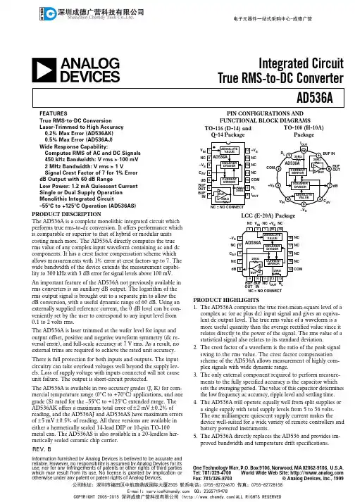
PIN CONFIGURATIONS AND FUNCTIONAL BLOCK DIAGRAMS TO-100 (H-10A) TO-116 (D-14) and Package Q-14 Package
The AD536A is a complete monolithic integrated circuit which performs true rms-to-dc conversion. It offers performance which is comparable or superior to that of hybrid or modular units costing much more. The AD536A directly computes the true rms value of any complex input waveform containing ac and dc components. It has a crest factor compensation scheme which allows measurements with 1% error at crest factors up to 7. The wide bandwidth of the device extends the measurement capability to 300 kHz with 3 dB error for signal levels above 100 mV. An important feature of the AD536A not previously available in rms converters is an auxiliary dB output. The logarithm of the rms output signal is brought out to a separate pin to allow the dB conversion, with a useful dynamic range of 60 dB. Using an externally supplied reference current, the 0 dB level can be conveniently set by the user to correspond to any input level from 0.1 to 2 volts rms. The AD536A is laser trimmed at the wafer level for input and output offset, positive and negative waveform symmetry (dc reversal error), and full-scale accuracy at 7 V rms. As a result, no external trims are required to achieve the rated unit accuracy. There is full protection for both inputs and outputs. The input circuitry can take overload voltages well beyond the supply levels. Loss of supply voltage with inputs connected will not cause unit failure. The output is short-circuit protected. The AD536A is available in two accuracy grades (J, K) for commercial temperature range (0°C to +70°C) applications, and one grade (S) rated for the –55°C to +125°C extended range. The AD536AK offers a maximum total error of ± 2 mV ± 0.2% of reading, and the AD536AJ and AD536AS have maximum errors of ± 5 mV ± 0.5% of reading. All three versions are available in either a hermetically sealed 14-lead DIP or 10-pin TO-100 metal can. The AD536AS is also available in a 20-leadless hermetically sealed ceramic chip carrier. REV. B
RL
25k⍀
BUF IN
25k⍀
AD536A
CURRENT MIRROR BUF
BUF OUT
SQUARER DIVIDER ABSOLUTE VALUE
dB
VIN –VS
CAV
NC = NO CONNECT
LCC (E-20A) Package
NC VIN NC +VS NC
3 2 1 20 19 18 17 16 25k⍀ CURRENT MIRROR 25k⍀ 11 12 13 15 14 ABSOLUTE VALUE
Information furnished by Analog Devices is believed to be accurate and reliable. However, no responsibility is assumed by Analog Devices for its use, nor for any infringements of patents or other rights of third parties which may result from its use. No license is granted by implication or otherwise under any patent or patent rights of Analog Devices.
a
FEATURES True RMS-to-DC Conversion Laser-Trimmed to High Accuracy 0.2% Max Error (AD536AK) 0.5% Max Error (AD536AJ) Wide Response Capability: Computes RMS of AC and DC Signals 450 kHz Bandwidth: V rms > 100 mV 2 MHz Bandwidth: V rms > 1 V Signal Crest Factor of 7 for 1% Error dB Output with 60 dB Range Low Power: 1.2 mA Quiescent Current Single or Dual Supply Operation Monolithic Integrated Circuit –55؇ C to +125؇ C Operation (AD536AS) PRODUCT DESCRIPTION
AD536A–SPECIFICATIONS (@ +25؇C, and ؎15 V dc unless otherwise noted)
Model Min TRANSFER FUNCTION CONVERSION ACCURACY Total Error, Internal Trim1 (Figure 1) vs. Temperature, TMIN to +70°C +70°C to +125°C vs. Supply Voltage dc Reversal Error Total Error, External Trim1 (Figure 2) ERROR VS. CREST FACTOR2 Crest Factor 1 to 2 Crest Factor = 3 Crest Factor = 7 FREQUENCY RESPONSE3 Bandwidth for 1% Additional Error (0.09 dB) VIN = 10 mV VIN = 100 mV VIN = 1 V ± 3 dB Bandwidth VIN = 10 mV VIN = 100 mV VIN = 1 V AVERAGlNG TlME CONSTANT (Figure 5) INPUT CHARACTERISTICS Signal Range, ± 15 V Supplies Continuous rms Level Peak Transient Input Continuous rms Level, ± 5 V Supplies Peak Transient Input, ± 5 V Supplies Maximum Continuous Nondestructive Input Level (All Supply Voltages) Input Resistance Input Offset Voltage OUTPUT CHARACTERISTICS Offset Voltage, VIN = COM (Figure 1) vs. Temperature vs. Supply Voltage Voltage Swing, ± 15 V Supplies ± 5 V Supply dB OUTPUT (Figure 13) Error, VlN 7 mV to 7 V rms, 0 dB = 1 V rms Scale Factor Scale Factor TC (Uncompensated, see Figure 1 for Temperature Compensation) IREF for 0 dB = 1 V rms IREF Range IOUT TERMINAL IOUT Scale Factor IOUT Scale Factor Tolerance Output Resistance Voltage Compliance BUFFER AMPLIFIER Input and Output Voltage Range Input Offset Voltage, RS = 25 k Input Bias Current Input Resistance Output Current Short Circuit Current Output Resistance Small Signal Bandwidth Slew Rate4 POWER SUPPLY Voltage Rated Performance Dual Supply Single Supply Quiescent Current Total VS , 5 V to 36 V, TMIN to TMAX TEMPERATURE RANGE Rated Performance Storage NUMBER OF TRANSISTORS 5 1 AD536AJ Typ V OUT = avg . (VIN )
ABSOLUTE VALUE 14 13 12 11 CURRENT MIRROR 25k⍀ BUF 25k⍀ 10 9 8
+VS NC NC NC COM RL IOUT
+VS COM
NC 2 AD536A –VS 3 CAV 4 dB 5 BUF OUT 6 BUF 7 IN
SQUARER DIVIDER
VIN 1
Integrated Circuit True RMS-to-DC Converter AD536A
PIN CONFIGURATIONS AND FUNCTIONAL BLOCK DIAGRAMS TO-100 (H-10A) TO-116 (D-14) and Package Q-14 Package
The AD536A is a complete monolithic integrated circuit which performs true rms-to-dc conversion. It offers performance which is comparable or superior to that of hybrid or modular units costing much more. The AD536A directly computes the true rms value of any complex input waveform containing ac and dc components. It has a crest factor compensation scheme which allows measurements with 1% error at crest factors up to 7. The wide bandwidth of the device extends the measurement capability to 300 kHz with 3 dB error for signal levels above 100 mV. An important feature of the AD536A not previously available in rms converters is an auxiliary dB output. The logarithm of the rms output signal is brought out to a separate pin to allow the dB conversion, with a useful dynamic range of 60 dB. Using an externally supplied reference current, the 0 dB level can be conveniently set by the user to correspond to any input level from 0.1 to 2 volts rms. The AD536A is laser trimmed at the wafer level for input and output offset, positive and negative waveform symmetry (dc reversal error), and full-scale accuracy at 7 V rms. As a result, no external trims are required to achieve the rated unit accuracy. There is full protection for both inputs and outputs. The input circuitry can take overload voltages well beyond the supply levels. Loss of supply voltage with inputs connected will not cause unit failure. The output is short-circuit protected. The AD536A is available in two accuracy grades (J, K) for commercial temperature range (0°C to +70°C) applications, and one grade (S) rated for the –55°C to +125°C extended range. The AD536AK offers a maximum total error of ± 2 mV ± 0.2% of reading, and the AD536AJ and AD536AS have maximum errors of ± 5 mV ± 0.5% of reading. All three versions are available in either a hermetically sealed 14-lead DIP or 10-pin TO-100 metal can. The AD536AS is also available in a 20-leadless hermetically sealed ceramic chip carrier. REV. B
RL
25k⍀
BUF IN
25k⍀
AD536A
CURRENT MIRROR BUF
BUF OUT
SQUARER DIVIDER ABSOLUTE VALUE
dB
VIN –VS
CAV
NC = NO CONNECT
LCC (E-20A) Package
NC VIN NC +VS NC
3 2 1 20 19 18 17 16 25k⍀ CURRENT MIRROR 25k⍀ 11 12 13 15 14 ABSOLUTE VALUE
Information furnished by Analog Devices is believed to be accurate and reliable. However, no responsibility is assumed by Analog Devices for its use, nor for any infringements of patents or other rights of third parties which may result from its use. No license is granted by implication or otherwise under any patent or patent rights of Analog Devices.
a
FEATURES True RMS-to-DC Conversion Laser-Trimmed to High Accuracy 0.2% Max Error (AD536AK) 0.5% Max Error (AD536AJ) Wide Response Capability: Computes RMS of AC and DC Signals 450 kHz Bandwidth: V rms > 100 mV 2 MHz Bandwidth: V rms > 1 V Signal Crest Factor of 7 for 1% Error dB Output with 60 dB Range Low Power: 1.2 mA Quiescent Current Single or Dual Supply Operation Monolithic Integrated Circuit –55؇ C to +125؇ C Operation (AD536AS) PRODUCT DESCRIPTION
AD536A–SPECIFICATIONS (@ +25؇C, and ؎15 V dc unless otherwise noted)
Model Min TRANSFER FUNCTION CONVERSION ACCURACY Total Error, Internal Trim1 (Figure 1) vs. Temperature, TMIN to +70°C +70°C to +125°C vs. Supply Voltage dc Reversal Error Total Error, External Trim1 (Figure 2) ERROR VS. CREST FACTOR2 Crest Factor 1 to 2 Crest Factor = 3 Crest Factor = 7 FREQUENCY RESPONSE3 Bandwidth for 1% Additional Error (0.09 dB) VIN = 10 mV VIN = 100 mV VIN = 1 V ± 3 dB Bandwidth VIN = 10 mV VIN = 100 mV VIN = 1 V AVERAGlNG TlME CONSTANT (Figure 5) INPUT CHARACTERISTICS Signal Range, ± 15 V Supplies Continuous rms Level Peak Transient Input Continuous rms Level, ± 5 V Supplies Peak Transient Input, ± 5 V Supplies Maximum Continuous Nondestructive Input Level (All Supply Voltages) Input Resistance Input Offset Voltage OUTPUT CHARACTERISTICS Offset Voltage, VIN = COM (Figure 1) vs. Temperature vs. Supply Voltage Voltage Swing, ± 15 V Supplies ± 5 V Supply dB OUTPUT (Figure 13) Error, VlN 7 mV to 7 V rms, 0 dB = 1 V rms Scale Factor Scale Factor TC (Uncompensated, see Figure 1 for Temperature Compensation) IREF for 0 dB = 1 V rms IREF Range IOUT TERMINAL IOUT Scale Factor IOUT Scale Factor Tolerance Output Resistance Voltage Compliance BUFFER AMPLIFIER Input and Output Voltage Range Input Offset Voltage, RS = 25 k Input Bias Current Input Resistance Output Current Short Circuit Current Output Resistance Small Signal Bandwidth Slew Rate4 POWER SUPPLY Voltage Rated Performance Dual Supply Single Supply Quiescent Current Total VS , 5 V to 36 V, TMIN to TMAX TEMPERATURE RANGE Rated Performance Storage NUMBER OF TRANSISTORS 5 1 AD536AJ Typ V OUT = avg . (VIN )