CS2540 灯珠数码管驱动芯片
- 格式:pdf
- 大小:568.36 KB
- 文档页数:8
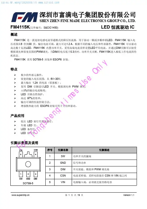
FM4115K(文件编号:S&CIC1450)LED恒流驱动IC概述FM4115K是一款连续电感电流导通模式的降压恒流源,用于驱动一颗或多颗串联LED。
FM4115K输入电压范围从6伏到30伏,输出电流可调,最大可达1.2A。
根据不同的输入电压和外部器件,FM4115K可以驱动高达数十瓦的LED。
FM4115K内置功率开关,采用高端电流采样设置LED平均电流,并通过DIM引脚可以接受模拟调光和很宽范围的PWM调光。
当DIM的电压低于0.3伏时,功率开关关断,FM4115K进入极低工作电流的待机状态。
FM4115K采用SOT89-5封装和ESOP8封装。
特点极少的外部元器件;很宽的输入电压范围:从6V~30V;最大输出1.2A的电流(铝基板);复用DIM引脚进行LED开关、模拟调光和PWM调光;±3%的输出电流精度;LED开路自然保护;高达97%的效率;输出可调的恒流控制方法;增强散热能力的ESOP8封装可用于大功率驱动。
产品应用低压LED射灯代替卤素灯;车载LED灯;LED备用灯;LED信号灯。
TongshengtimesUseOnlyFM4115K (文件编号:S&CIC1450)LED 恒流驱动ICESOP-8功能模块图F o rT o ng s he n g t im e sFM4115K (文件编号:S&CIC1450)LED 恒流驱动IC参数特性注1:最大极限值是指超出该工作范围,芯片有可能损坏。
推荐工作范围是指在该范围内,器件功能正常,但并不完全保证满足个别性能指标。
电气参数定义了器件在工作范围内并且在保证特定性能指标的测试条件下的直流和交流电参数规范。
对于未给定上下限值的参数,该规范不予保证其精度,但其典型值合理反映了器件性能。
注2:温度升高最大功耗一定会减小,这也是由T JMAX ,θJA ,和环境温度T A 所决定的。
最大允许功耗为:P DMAX =(T JMAX -T A )/θJA 或是极限范围给出的数字中比较低的那个值。
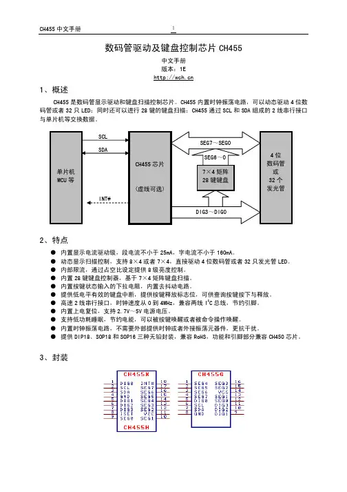
数码管驱动及键盘控制芯片CH455中文手册版本:1E1、概述CH455是数码管显示驱动和键盘扫描控制芯片。
CH455内置时钟振荡电路,可以动态驱动4位数码管或者32只LED;同时还可以进行28键的键盘扫描;CH455通过SCL和SDA组成的2线串行接口与单片机等交换数据。
2、特点●内置显示电流驱动级,段电流不小于25mA,字电流不小于160mA。
●动态显示扫描控制,支持8×4或者7×4,直接驱动4位数码管或者32只发光管LED。
●内部限流,通过占空比设定提供8级亮度控制。
●内置28键键盘控制器,基于7×4矩阵键盘扫描。
●内置按键状态输入的下拉电阻,内置去抖动电路。
●提供低电平有效的键盘中断,提供按键释放标志位,可供查询按键按下与释放。
●高速2线串行接口,时钟速度从0到4MHz,兼容两线I2C总线,节约引脚。
●内置上电复位,支持2.7V~5V电源电压。
●支持低功耗睡眠,节约电能,可以被按键唤醒或者被命令操作唤醒。
●内置时钟振荡电路,不需要外部提供时钟或者外接振荡元器件,更抗干扰。
●提供DIP18、SOP18和SOP16三种无铅封装,兼容RoHS,功能和引脚部分兼容CH450芯片。
3、封装封装形式宽度引脚间距封装说明订货型号DIP18 7.62mm 300mil 2.54mm 100mil 标准18脚双列直插CH455K SOP18 7.62mm 300mil 1.27mm 50mil 标准的宽18脚贴片CH455H SOP16 3.9mm 150mil 1.27mm 50mil 标准的16脚贴片CH455G4、引脚引脚号引脚名称类型引脚说明DIP18/SOP18 SOP1611 14 VCC 电源正电源,持续电流不小于150mA4 8 GND 电源公共接地,持续电流不小于150mA9、10 12、13 14、15 16 12、1315、161、23SEG0~SEG6三态输出及输入数码管的段驱动,高电平有效,键盘扫描输入,高电平有效,内置下拉17 4 SEG7 输出数码管的小数点段驱动输出,高电平有效,7段模式下的键盘中断输出,低电平有效1、5 6、75、910、11DIG0~DIG3输出数码管的字驱动,低电平有效,键盘扫描输出,高电平有效3 7 SDA 内置上拉开漏输出及输入2线串行接口的数据输入和输出,内置上拉电阻2 6 SCL 输入2线串行接口的数据时钟,内置上拉电阻18 无INT# 内置上拉开漏输出键盘中断输出,低电平有效8 无ISET 输入段电流上限调整,悬空为默认设置5、功能说明5.1. 一般说明本手册中的数据,以B结尾的为二进制数,以H结尾的为十六进制数,否则为十进制数,标注为x的位表示该位可以是任意值。
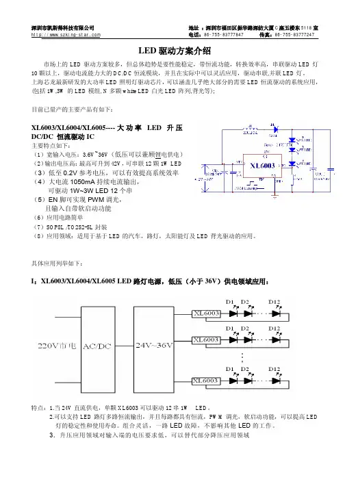
LED 驱动方案介绍市场上的LED 驱动方案较多,但总体趋势是要性能稳定,带恒流功能,转换效率高,串联驱动LED 灯10颗以上,驱动电流能力大的DC/DC 恒流模块,并且在实际中可以灵活应用,驱动串联,并联LED 灯。
上海芯龙最新研发的大功率LED 照明灯驱动芯片,可以涵盖几乎绝大部分的需要LED 恒流驱动的系统应用,(包括1W,3W 的LED 模组, N 多颗white LED 白光LED 阵列,背光等);目前已量产的主要产品有如下:XL6003/XL6004/XL6005----大功率LED 升压DC/DC 恒流驱动IC主要特点如下:(1)宽输入电压:3.6V~36V (低压可以兼顾锂电供电)(2)输出电压高:最高可升到42V ,可串联12颗1W LED(3)低至0.2V 参考电压,可以有效提高系统效率 (4)大电流1050mA 持续电流输出,可驱动1W~3W LED 12个串 (5)EN 脚可实现PWM 调光,且输入自带软启动功能(6)应用电路简单(7)SOP8L /TO252-5L 封装(8)应用领域:适用于基于LED 的汽车,路灯,太阳能灯及LED 背光驱动的应用。
具体应用列举如下:I :XL6003/XL6004/XL6005 LED 路灯电源,低压(小于36V )供电领域应用:特点:1.当24V 直流供电,单颗XL6003可以驱动12串1W LED 。
2.可以支持LED 路灯多路恒流输出,并且每路都具有恒流,PWM 调光,软启动功能,可以提高LED 灯的稳定性和使用寿命。
组合灵活,一路LED 故障,不影响其他LED 的工作。
3.升压应用领域对输入端的电压要求低,可以替代部分降压应用领域II :XL6003/XL6004/XL6005 太阳能LED 灯电源应用:0.5W~3W LED 灯太阳能LED 电源驱动方案60mW LED 阵列太阳能LED 电源驱动方案特点:1. XL6003/XL6004/XL6005是升压DC/DC 恒流驱动IC ,12V 蓄电池电压通过XL6003升压可以驱动12颗串联1W LED 灯。
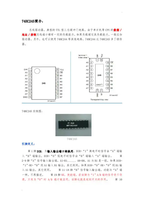
74HC245简介:总线驱动器,典型的TTL型三态缓冲门电路。
由于单片机等CPU的数据/地址/控制总线端口都有一定的负载能力,如果负载超过其负载能力,一般应加驱动器。
另外,也可以使用74HC244等其他电路,74HC244比74HC245多了锁存器。
74HC245实物图:74HC245引脚定义:第1脚DIR,为输入输出端口转换用,DIR=“1”高电平时信号由“A”端输入“B”端输出,DIR=“0”低电平时信号由“B”端输入“A”端输出。
第2-9脚“A”信号输入输出端,A1=B1、、、、、、A8=B8,A1与B1是一组,如果DIR=“1”OE=“0”则A1输入B1输出,其它类同。
如果DIR=“0”OE=“0”则B1输入A1输出,其它类同。
第11-18脚“B”信号输入输出端,功能与“A”端一样,不再描述。
第19脚OE,使能端,若该脚为“1”A/B端的信号将不导通,只有为“0”时A/B端才被启用,该脚也就是起到开关的作用。
第10脚GND,电源地。
第20脚VCC,电源正极。
TRUTH TABLE真值表Control Inputs 控制输入Operation 运行G DIRL L B 数据到A 总线L H A 数据到B 总线H X 隔开H=高电平 L=低电平×=不定Absolute Maximum Ratings绝对最大额定值Supply Voltage电源电压(VCC) -0.5 to -7.0V DC Input Voltage DIR and G pins (VIN) 直流输入电压方向和G引脚(输入电压)-1.5 to VCC -1.5V DC Input/Output Voltage (VIN, VOUT)直流输入/输出电压-0.5 to VCC -0.5V Clamp Diode Current 钳位二极管电流(ICD) ±20 mA DC Output Current直流输出电流,每个引脚(输出)±35 mA DC VCC or GND Current, per pin (ICC) ±70 mA Storage Temperature Range 储存温度范围(TSTG) -65℃ to -150℃Power Dissipation (PD)功耗(Note 3) 600 mW S.O. Package only 500 mW Lead Temperature (TL) (Soldering 10 seconds) 260℃【74HC245的作用:信号功率放大。
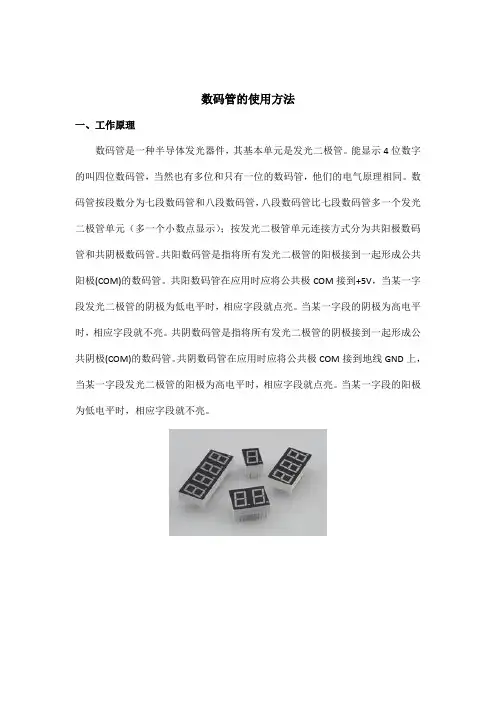
数码管的使用方法一、工作原理数码管是一种半导体发光器件,其基本单元是发光二极管。
能显示4位数字的叫四位数码管,当然也有多位和只有一位的数码管,他们的电气原理相同。
数码管按段数分为七段数码管和八段数码管,八段数码管比七段数码管多一个发光二极管单元(多一个小数点显示);按发光二极管单元连接方式分为共阳极数码管和共阴极数码管。
共阳数码管是指将所有发光二极管的阳极接到一起形成公共阳极(COM)的数码管。
共阳数码管在应用时应将公共极COM接到+5V,当某一字段发光二极管的阴极为低电平时,相应字段就点亮。
当某一字段的阴极为高电平时,相应字段就不亮。
共阴数码管是指将所有发光二极管的阴极接到一起形成公共阴极(COM)的数码管。
共阴数码管在应用时应将公共极COM接到地线GND上,当某一字段发光二极管的阳极为高电平时,相应字段就点亮。
当某一字段的阳极为低电平时,相应字段就不亮。
万联芯城-电子元器件采购网一直秉承着以良心做好良芯的服务理念,为广大客户提供一站式的电子元器件配单服务,客户行业涉及电子电工,智能工控,自动化,医疗安防等多个相关研发生产领域,所售电子元器件均为原厂渠道进货的原装现货库存。
只需提交BOM表,即可为您报价。
万联芯城同时为长电,顺络,先科ST等知名原厂的指定授权代理商,采购代理品牌电子元器件价格更有优势,欢迎广大客户咨询,点击进入万联芯城。
二、电气特性单位数码管有十个管脚,其中有8根是用来点亮a,b,c,d,e,f,dp 共8个发光二极管(原理中有介绍),3,8两个管脚为公共COM脚,它们相连通且作用相同,可接任意一根。
为了更清楚介绍,贴图如下:三、驱动方式静态驱动也称直流驱动。
静态驱动是指每个数码管的每一个段码都由一个单片机的I/O端口进行驱动,或者使用如BCD码二-十进制译码器译码进行驱动。
静态驱动的优点是编程简单,显示亮度高,缺点是占用I/O端口多,如驱动5个数码管静态显示则需要5×8=40根I/O端口来驱动,要知道一个89S51单片机可用的I/O端口才32个呢:),实际应用时必须增加译码驱动器进行驱动,增加了硬件电路的复杂性。
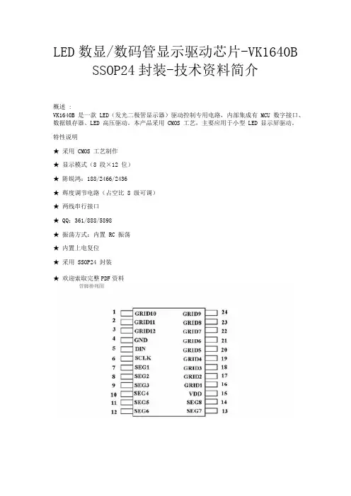
LED数显/数码管显示驱动芯片-VK1640B SSOP24封装-技术资料简介概述 :VK1640B 是一款 LED(发光二极管显示器)驱动控制专用电路,内部集成有 MCU 数字接口、数据锁存器、LED 高压驱动。
本产品采用 CMOS 工艺,主要应用于小型 LED 显示屏驱动。
特性说明★采用 CMOS 工艺制作★显示模式(8 段×12 位)★陈锐鸿:188/2466/2436★辉度调节电路(占空比 8 级可调)★两线串行接口★ QQ:361/888/5898★振荡方式:内置 RC 振荡★内置上电复位★采用 SSOP24 封装★欢迎索取完整PDF资料——————————————————————LCD/LED液晶控制器及驱动器系列芯片简介如下:RAM映射LCD控制器和驱动器系列:VK1024B 2.4~5.2V SEG*COM:6*4、6*3、6*2 偏置电压1/2 1/3 S0P-16VK1056B 2.4~5.2V SEG*COM:14*4、14*3/14*2偏置电压1/2 1/3 SOP/SSOP24 VK1072B 2.4~5.2V SEG*COM:18*4、18*3、18*2偏置电压1/2 1/3 SOP28VK1072C 2.4~5.2V SEG*COM:18*4、18*3、18*2偏置电压1/2 1/3 SOP28VK1072D 2.4~5.2V SEG*COM:18*4、18*3、18*2偏置电压1/2 1/3 SSOP28 VK1088B 2.4~5.2V SEG*COM:22*4、22*3、22*2 偏置电压1/2 1/3 QFN32(4*4) VK0192 2.4~5.2V 24seg*8com 偏置电压1/4 LQFP-44VK0256 2.4~5.2V 32seg*8com 偏置电压1/4 QFP-64VK0256B 2.4~5.2V 32seg*8com 偏置电压1/4 LQFP-64VK0256C 2.4~5.2V 32seg*8com 偏置电压1/4 LQFP-52VK1621 2.4~5.2V SEG*COM:32*4、32*3、32*2偏置电压1/2 1/3 LQFP44/48/SSOP48/SKY28/DICE裸片VK1622 2.4~5.5V 32seg*8com偏置电压1/4 LQFP44/48/52/64/QFP64/DICE裸片VK1623 2.4~5.2V 48seg*8com偏置电压1/4 LQFP-100/QFP-100/DICE裸片VK1625 2.4~5.2V 64seg*8com偏置电压1/4 LQFP-100/QFP-100/DICE 裸片VK1626 2.4~5.2V 48seg*16com偏置电压1/5 LQFP-100/QFP-100/DICE 裸片——————————————————————————————————高抗干扰LCD液晶控制器及驱动系列:VK2C21A 2.4~5.5V 20seg*4com 16*8 偏置电压1/3 1/4 I2C通讯接口 SOP-28VK2C21B 2.4~5.5V 16seg*4com 12*8 偏置电压1/3 1/4 I2C通讯接口 SOP-24VK2C21C 2.4~5.5V 12seg*4com 8*8 偏置电压1/3 1/4 I2C通讯接口 SOP-20VK2C21D 2.4~5.5V 8seg*4com 4*8 偏置电压1/3 1/4 I2C通讯接口 SOP-16VK2C22A 2.4~5.5V 44seg*4com 偏置电压1/2 1/3 I2C通讯接口 LQFP-52VK2C22B 2.4~5.5V 40seg*4com 偏置电压1/2 1/3 I2C通讯接口 LQFP-48VK2C23A 2.4~5.5V 56seg*4com 52*8 偏置电压1/3 1/4 I2C通讯接口 LQFP-64VK2C23B 2.4~5.5V 36seg*8com 偏置电压1/31/4 I2C通讯接口 LQFP-48VK2C24 2.4~5.5V 72seg*4com 68*8 60*16 偏置电压1/3 1/4 1/5 I2C通讯接口 LQFP-80超低功耗LCD液晶控制器及驱动系列:VKL060 2.5~5.5V 15seg*4com 偏置电压1/2 1/3 I2C通讯接口SSOP-24VKL128 2.5~5.5V 32seg*4com 偏置电压1/2 1/3 I2C通讯接口LQFP-44VKL144A 2.5~5.5V 36seg*4com 偏置电压1/2 1/3 I2C通讯接口TSSOP-48VKL144B 2.5~5.5V 36seg*4com 偏置电压1/21/3 I2C通讯接口QFN48L (6MM*6MM)静态显示LCD液晶控制器及驱动系列:VKS118 2.4~5.2V 118seg*2com 偏置电压 -- 4线通讯接口LQFP-128VKS232 2.4~5.2V 116seg*2com 偏置电压1/1 1/2 4线通讯接口LQFP-128内存映射的LED控制器及驱动器VK1628---通讯接口:STb/CLK/DIO 电源电压:5V(4.5~5.5V) 驱动点阵:70/52共阴驱动:10段7位/13段4位共阳驱动:7段10位按键:10x2 封装SOP28VK1629---通讯接口:STb/CLK/DIN/DOUT 电源电压:5V(4.5~5.5V) 驱动点阵:128共阴驱动:16段8位共阳驱动:8段16位按键:8x4 封装QFP44VK1629A---通讯接口:STb/CLK/DIO 电源电压:5V(4.5~5.5V) 驱动点阵:128共阴驱动:16段8位共阳驱动:8段16位按键:--- 封装SOP32VK1629B---通讯接口:STb/CLK/DIO 电源电压:5V(4.5~5.5V) 驱动点阵:112共阴驱动:14段8位共阳驱动:8段14位按键:8x2 封装SOP32VK1629C---通讯接口:STb/CLK/DIO 电源电压:5V(4.5~5.5V) 驱动点阵:120共阴驱动:15段8位共阳驱动:8段15位按键:8x1 封装SOP32VK1629D---通讯接口:STb/CLK/DIO 电源电压:5V(4.5~5.5V) 驱动点阵:96共阴驱动:12段8位共阳驱动:8段12位按键:8x4 封装SOP32VK1640---通讯接口: CLK/DIN 电源电压:5V(4.5~5.5V) 驱动点阵:128共阴驱动:8段16位共阳驱动:16段8位按键:--- 封装SOP28VK1640A---通讯接口: CLK/DIN 电源电压:5V(4.5~5.5V) 驱动点阵:128共阴驱动:8段16位共阳驱动:16段8位按键:--- 封装SSOP28VK1640B---通讯接口: CLK/DIN 电源电压:5V(4.5~5.5V) 驱动点阵:96 共阴驱动:8段12位共阳驱动:12段8位按键:--- 封装SSOP24VK1650---通讯接口: SCL/SDA 电源电压:5V(3.0~5.5V)共阴驱动:8段4位共阳驱动:4段8位按键:7x4 封装SOP16/DIP16VK1651---通讯接口: SCL/SDA 电源电压:5V(3.0~5.5V)共阴驱动:7段4位共阳驱动:4段7位按键:7x1 封装SOP16/DIP16VK1616---通讯接口: 三线串行电源电压:5V(3.0~5.5V)显示模式:7段4位按键:7x1 封装SOP16/DIP16VK1668---通讯接口:STb/CLK/DIO 电源电压:5V(4.5~5.5V) 驱动点阵:70/52共阴驱动:10段7位/13段4位共阳驱动:7段10位按键:10x2 封装SOP24VK6932---通讯接口:STb/CLK/DIN 电源电压:5V(4.5~5.5V) 驱动点阵:128共阴驱动:8段16位17.5/140mA 共阳驱动:16段8位按键:--- 封装SOP32VK16K33A/B/C---通讯接口:SCL/SDA 电源电压:5V(4.5V~5.5V)驱动点阵:128/96/64共阴驱动:16段8位/12段8位/8段8位共阳驱动:8段16位/8段12位/8段8位按键:13x3 10x3 8x3封装SOP20/SOP24/SOP28VK1618---带键盘扫描接口的LED驱动控制专用电路,内部集成有MCU数字接口、数据锁存器、键盘扫描等电路共阴驱动:5段7位/6段6位/7段5位/8段4位共阳驱动:7段5位/6段6位/5段7位/4段8位按键:5x1 封装SOP18/DIP18VK1S68C---LED驅動IC 10x7/13x4段位10段7位/11段6位共阴10x2按键,封装SSOP24VK1Q68D---LED驅動IC 10x7/13x4段位10段7位/11段6位共阴10x2按键,封装QFP24VK1S38A---LED驱动IC 8段×8位封装SSOP24VK1638--- LED驱动IC 共阴10段8位共阳8段10位封装SOP32——————————————————————————————————触摸触控IC系列简介如下:标准触控IC-电池供电系列:VKD223EB --- 工作电压/电流:2.0V-5.5V/5uA-3V 感应通道数:1 通讯接口最长响应时间快速模式60mS,低功耗模式220ms 封装:SOT23-6VKD223B --- 工作电压/电流:2.0V-5.5V/5uA-3V 感应通道数:1通讯接口最长响应时间快速模式60mS,低功耗模式220ms 封装:SOT23-6VKD233DB ---工作电压/电流:2.4V-5.5V/2.5uA-3V 1感应按键封装:SOT23-6 通讯接口:直接输出,锁存(toggle)输出低功耗模式电流2.5uA-3VVKD233DH ---工作电压/电流:2.4V-5.5V/2.5uA-3V 1感应按键封装:SOT23-6 通讯接口:直接输出,锁存(toggle)输出有效键最长时间检测16SVKD233DS ---工作电压/电流:2.4V-5.5V/2.5uA-3V 1感应按键封装:DFN6通讯接口:直接输出,锁存(toggle)输出低功耗模式电流2.5uA-3VVKD233DR ---工作电压/电流:2.4V-5.5V/1.5uA-3V 1感应按键封装:DFN6 通讯接口:直接输出,锁存(toggle)输出低功耗模式电流1.5uA-3VVKD233DG --- 工作电压/电流:2.4V-5.5V/2.5uA-3V 1感应按键封装:DFN6 通讯接口:直接输出,锁存(toggle)输出低功耗模式电流2.5uA-3VVKD233DQ --- 工作电压/电流:2.4V-5.5V/5uA-3V 1感应按键封装:SOT23-6通讯接口:直接输出,锁存(toggle)输出低功耗模式电流5uA-3VVKD233DM --- 工作电压/电流:2.4V-5.5V/5uA-3V 1感应按键封装:SOT23-6 (开漏输出)通讯接口:开漏输出,锁存(toggle)输出低功耗模式电流5uA-3VVKD232C--- 工作电压/电流:2.4V-5.5V/2.5uA-3V 感应通道数:2 封装:SOT23-6通讯接口:直接输出,低电平有效固定为多键输出模式,內建稳压电路——————————————————————————————————MTP触摸IC——VK36N系列抗电源辐射及手机干扰:VK3601L --- 工作电压/电流:2.4V-5.5V/4UA-3V3 感应通道数:1 1对1直接输出待机电流小,抗电源及手机干扰,可通过CAP调节灵敏封装:SOT23-6VK36N1D --- 工作电压/电流:2.2V-5.5V/7UA-3V3 感应通道数:1 1对1直接输出触摸积水仍可操作,抗电源及手机干扰,可通过CAP调节灵敏封装:SOT23-6VK36N2P --- 工作电压/电流:2.2V-5.5V/7UA-3V3 感应通道数:2 脉冲输出触摸积水仍可操作,抗电源及手机干扰,可通过CAP调节灵敏封装:SOT23-6VK3602XS ---工作电压/电流:2.4V-5.5V/60UA-3V 感应通道数:2 2对2锁存输出低功耗模式电流8uA-3V,抗电源辐射干扰,宽供电电压封装:SOP8VK3602K --- 工作电压/电流:2.4V-5.5V/60UA-3V 感应通道数:2 2对2直接输出低功耗模式电流8uA-3V,抗电源辐射干扰,宽供电电压封装:SOP8VK36N2D --- 工作电压/电流:2.2V-5.5V/7UA-3V3 感应通道数:2 1对1直接输出触摸积水仍可操作,抗电源及手机干扰,可通过CAP调节灵敏封装:SOP8VK36N3BT ---工作电压/电流:2.2V-5.5V/7UA-3V3 感应通道数:3 BCD码锁存输出触摸积水仍可操作,抗电源及手机干扰,可通过CAP调节灵敏封装:SOP8VK36N3BD ---工作电压/电流:2.2V-5.5V/7UA-3V3 感应通道数:3 BCD码直接输出触摸积水仍可操作,抗电源及手机干扰,可通过CAP调节灵敏封装:SOP8VK36N3BO ---工作电压/电流:2.2V-5.5V/7UA-3V3 感应通道数:3 BCD码开漏输出触摸积水仍可操作,抗电源及手机干扰封装:SOP8/DFN8(超小超薄体积)VK36N3D --- 工作电压/电流:2.2V-5.5V/7UA-3V3 感应通道数:3 1对1直接输出触摸积水仍可操作,抗电源及手机干扰封装:SOP16/DFN16(超小超薄体积)VK36N4B ---工作电压/电流:2.2V-5.5V/7UA-3V3 感应通道数:4 BCD输出触摸积水仍可操作,抗电源及手机干扰封装:SOP16/DFN16(超小超薄体积)VK36N4I---工作电压/电流:2.2V-5.5V/7UA-3V3 感应通道数:4 I2C输出触摸积水仍可操作,抗电源及手机干扰封装:SOP16/DFN16(超小超薄体积)VK36N5D ---工作电压/电流:2.2V-5.5V/7UA-3V3 感应通道数:5 1对1直接输出触摸积水仍可操作,抗电源及手机干扰封装:SOP16/DFN16(超小超薄体积)VK36N5B ---工作电压/电流:2.2V-5.5V/7UA-3V3 感应通道数:5 BCD输出触摸积水仍可操作,抗电源及手机干扰封装:SOP16/DFN16(超小超薄体积)VK36N5I ---工作电压/电流:2.2V-5.5V/7UA-3V3 感应通道数:5 I2C输出触摸积水仍可操作,抗电源及手机干扰封装:SOP16/DFN16(超小超薄体积)VK36N6D --- 工作电压/电流:2.2V-5.5V/7UA-3V3 感应通道数:6 1对1直接输出触摸积水仍可操作,抗电源及手机干扰封装:SOP16/DFN16(超小超薄体积)VK36N6B ---工作电压/电流:2.2V-5.5V/7UA-3V3 感应通道数:6 BCD输出触摸积水仍可操作,抗电源及手机干扰封装:SOP16/DFN16(超小超薄体积)VK36N6I ---工作电压/电流:2.2V-5.5V/7UA-3V3 感应通道数:6 I2C输出触摸积水仍可操作,抗电源及手机干扰封装:SOP16/DFN16(超小超薄体积)VK36N7B ---工作电压/电流:2.2V-5.5V/7UA-3V3 感应通道数:7 BCD输出触摸积水仍可操作,抗电源及手机干扰封装:SOP16/DFN16(超小超薄体积)VK36N7I ---工作电压/电流:2.2V-5.5V/7UA-3V3 感应通道数:7 I2C输出触摸积水仍可操作,抗电源及手机干扰封装:SOP16/DFN16(超小超薄体积)VK36N8B ---工作电压/电流:2.2V-5.5V/7UA-3V3 感应通道数:8 BCD输出触摸积水仍可操作,抗电源及手机干扰封装:SOP16/DFN16(超小超薄体积)VK36N8I ---工作电压/电流:2.2V-5.5V/7UA-3V3 感应通道数:8 I2C输出触摸积水仍可操作,抗电源及手机干扰封装:SOP16/DFN16(超小超薄体积)VK36N9I ---工作电压/电流:2.2V-5.5V/7UA-3V3 感应通道数:9 I2C输出触摸积水仍可操作,抗电源及手机干扰封装:SOP16/DFN16(超小超薄体积)VK36N10I ---工作电压/电流:2.2V-5.5V/7UA-3V3 感应通道数:10 I2C输出触摸积水仍可操作,抗电源及手机干扰封装:SOP16/DFN16(超小超薄体积)——————————————————————————————————1-8点高灵敏度液体水位检测IC——VK36W系列VK36W1D ---工作电压/电流:2.2V-5.5V/10UA-3V3 1对1直接输出水位检测通道:1可用于不同壁厚和不同水质水位检测,抗电源/手机干扰封装:SOT23-6备注:1. 开漏输出低电平有效2、适合需要抗干扰性好的产品应用VK36W2D ---工作电压/电流:2.2V-5.5V/10UA-3V3 1对1直接输出水位检测通道:2可用于不同壁厚和不同水质水位检测,抗电源/手机干扰封装:SOP8备注:1. 1对1直接输出 2、输出模式/输出电平可通过IO选择VK36W4D ---工作电压/电流:2.2V-5.5V/10UA-3V3 1对1直接输出水位检测通道:4可用于不同壁厚和不同水质水位检测,抗电源/手机干扰封装:SOP16/DFN16 备注:1. 1对1直接输出 2、输出模式/输出电平可通过IO选择VK36W6D ---工作电压/电流:2.2V-5.5V/10UA-3V3 1对1直接输出水位检测通道:6可用于不同壁厚和不同水质水位检测,抗电源/手机干扰封装:SOP16/DFN16 备注:1. 1对1直接输出2、输出模式/输出电平可通过IO选择VK36W8I ---工作电压/电流:2.2V-5.5V/10UA-3V3 I2C输出水位检测通道:8可用于不同壁厚和不同水质水位检测,抗电源/手机干扰封装:SOP16/DFN16。
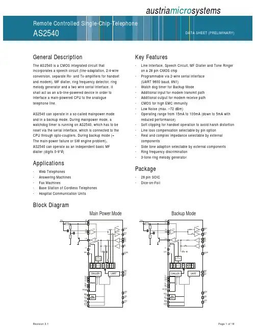
Data Sheet AS2540austria micro systemsaustria micro systemsGeneral DescriptionThe AS2540 is a CMOS integrated circuit that incorporates a speech circuit (line-adaptation, 2/4-wire conversion, separate Rx- and Tx-amplifiers for handset and modem), MF dialler, ring frequency detector, ring melody generator and a two wire serial interface. It shall act as an a/b-line-powered device in order to interface a main-powered CPU to the analogue telephone line.AS2540 can operate in a so-called mainpower mode and in a backup mode. During mainpower mode, a watchdog timer is running on AS2540, which has to be reset via the serial interface, which is connected to the CPU through opto-couplers. During backup mode (= The main-power failure or SW engine problem),AS2540 can operate as an independent basic MF dialler (digits 0-9*#)Applications-Web Telephones-Answering Machines-Fax Machines-Base Station of Cordless Telephones-Hospital Communication Units Key Features-Line Interface, Speech Circuit, MF Dialler and Tone Ringer on a 28 pin CMOS chip-Programmable via 2-wire serial interface(UART 9600 baud, 8N1)-Watch dog timer for Backup Mode-Additional input for modem transmit path-Additional output for modem receive path-CMOS for high EMC immunity-Low Noise (max. –72 dBm)-Operating range from 15mA to 100mA (down to 5mA with reduced performance)-Soft clipping for handset operation to avoid harsh distortion -Line loss compensation selectable by pin option-Real and complex impedance selectable by external components-Side tone adaption selectable by external components-Ring frequency discrimination-3-tone ring melody generatorPackage-28 pin SOIC-Dice-on-FoilBlock DiagramMain Power Mode Backup ModePin Description15RFD R ing F requency D iscriminationSchmitt trigger input for ring frequency discrimination. Disabled during off-hook.7LS L ine Current S ense InputInput for sensing the line current5LI L ine I nputInput used for power extraction and line current sensing6RI R eceive I nputInput for ac-separated receive signal2STB S ide T one B alance InputInput for side tone cancellation network3CS C urrent S hunt Control OutputN-channel open drain output to control the external high power shunt transistor for synthesising ac- anddc- impedance, modulation of line voltage and shorting the line during make periods of pulse dialling8CI C omplex I mpedance InputInput pin for the capacitor to program a complex impedance16DPn D ial P ulse OutputOpen drain output pulls low during break periods of pulse dialling and flash17EHS E lectronic H ook S witchSchmitt Trigger Input to detect an electronic off-hook.18MHS M anual H ook S witchSchmitt Trigger Input to detect a manual off-hook.19MODE D TMF L evel S election-4/-6dBm—>DLS open-6/-8dBm—>DLS-r1-8/-10dBm—>DLS-r2L ine L oss C ompensation Select Pin45mA-75mA—>LLC open20mA-50mA—>LLC-r3None—>LLC-r428MO Ring M elody O utputPDM output of the ring melody generator.11VDD V oltage D rain D rainPositive Power Supply4VSS V oltage S ource S ourceNegative Power Supply25OSC O scillator InputInput for ceramic resonator 3.58MHz.Recommended type: Murata CSA 3.58MG312AM or compatible12AGND A nalogue G roundSpecial ground for the internal amplifiers26RXD R eceive D ata InputSchmitt trigger input to serial interface27TXD T ransmit D ata OutputOpen drain output from serial interface20 21R1R2Keyboard R ows22 23 24C1C2C3Keyboard C olumns10ROT R eceive O utput to T ransformerOutput for driving a transformer with an ac impedance larger than 10kΩ1TIT T ransformer I nput from T ransformerSingle ended input for transformer9ROH R eceive O utput to H andsetOutput for driving a dynamic earpiece with an impedance from 150Ω to 300Ω13 14M2M1M icrophone InputsDifferential inputs for the microphone (electret)Functional DescriptionModes of operationThere are 4 possible modes:Idle ModeManual hook-switch and electronic hook-switch (e.g. relay) is open (MHS ∩ EHS = logical 0), no ring signal is applied, the oscillator is stopped, signalling via the serial interface is not possible.Ringing ModeAS2540 is supplied via the ring capacitor and external path, manual hook -switch and electronic hook-switch is open (MHS ∩ EHS = logical 0), the oscillator is running, a valid incoming ringing is signalled via the serial interface to the CPU. If the CPU does not reply the AS2540 switches into backup mode and sends a ring melody to the MO output.Backup ModeManual hook-switch and/or electronic hook-switch is closed (MHS ∪ EHS = logical 1), AS2540 is supplied with line current, the oscillator is running, the keyscan is enabled and the handset path is switched on, signalling via the serial interface is possible. After AS2540 has started dialling in backup mode, he must not be interrupted any more in order to ensure consistent dialling. A mode transition BM -> MPM is only possible before AS2540 has started dialling digits independently.Main Power ModeManual hook-switch and/or electronic hook-switch is closed, AS2540 is supplied with line current (MHS ∪ EHS = logical 1), the oscillator is running, the keyscan is disabled, AS2540 is controlled via the serial interface, handset path or monitor path or modem path is on, signalling via the serial interface is possible.Select Operation Mode<SetHandsetPath>SROH SROT & STIT <SetModemPath>SROT & STIT<SetMonitorPath>SROH & SROT STIT Example Main Power ModeStart-up in backup modeAs soon as AS2540 is supplied with line current, the external V dd capacitor will be charged up via the LI and VDD pin and after the V dd voltage has reached the operating level, the handset path of the speech circuit is switched on. This off-hook status is also signalled to the internal logic via the MHS or EHS pin in order to start the pinscan and subsequently set the country specific modes. Additionally a <LineEvent> message is sent to the CPU.Start-up in ring modeWhen a ringing signal is applied to the line, V dd of AS2540 is charged up via an external path. After V dd has reached the operating voltage the oscillator starts and AS2540 discriminates the ring frequency. After a valid ring frequency is applied on the RFD pin, the logic sends a<LineEvent> message is sent to the CPU and a watchdog timer is started. When the <LineEvent> message is not quit by the CPU before the watchdog timer has finished the countdown, AS2540 changes into backup mode and sends out a melody via the MO pin.DC conditionsThe normal operating mode is from 15mA to 100mA. An operating mode with reduced performance is from 5mA to 15mA. In the line hold range from 0mA to 5mA the device is in a power down mode and the voltage at LI is reduced to a maximum of 3.5VReceive pathThe gain of the LS —> ROH receive path is set to 2dB for ac-impedance 1000Ω. The receive input is the differentialsignal of RI and STB. During DTMF dialling a MF comfort tone is applied to ROH which is -30dB relative to the line level. The soft clip circuit limits the output voltage at ROH to 1V p. It prevents harsh distortion and acoustic shock.The gain of the LS —> ROT receive path is set to 0dB for ac-impedance 1000Ω. The receive input is the differential signal of RI and STB. The soft clip circuit is not active for this output.ModescanThe DTMF-level on the line and the function of the line loss compensation can be selected with the connection of the MODE-pin to the keyboard matrix. The MODE-pin is scanned once after each OFF-Hook transition.C3C2C1R2R1LLC Dtmf Level 45mA-75mA -6dBm XX45mA-75mA -8dBm X45mA-75mA -10dBm X20mA-50mA -6dBm X20mA-50mA-8dBm X X 20mA-50mA -10dBm XXNo LLC -6dBm X X No LLC -8dBm XXX No LLC-10dBmX indicates connection to pin modeSerial interfaceThe communication principle is derived from a standard UART: -Baud Rate9600-Start Bit1-Data Bits8-Parity None-Stop Bit1-LSB is transferred prior to MSBRx - messagesX MSB X d5d4d3d2d11LSBx x010101Digit 0Starts DTMF dialling of digit x x000011Digit 1Starts DTMF dialling of digit x x000101Digit 2Starts DTMF dialling of digit x x000111Digit 3Starts DTMF dialling of digit x x001001Digit 4Starts DTMF dialling of digit x x001011Digit 5Starts DTMF dialling of digit x x001101Digit 6Starts DTMF dialling of digit x x001111Digit 7Starts DTMF dialling of digit x x010001Digit 8Starts DTMF dialling of digit x x010011Digit 9Starts DTMF dialling of digit x x010111Digit *Starts DTMF dialling of digit x x000001Digit #Starts DTMF dialling of digit x x011001Digit A Starts DTMF dialling of digit x x011011Digit B Starts DTMF dialling of digit x x011101Digit C Starts DTMF dialling of digit x x011111Digit D Starts DTMF dialling of digit x x100001KeyReleased Stops Diallingx x101101SetDPn_HIGH Release pin Dpn (open drain) x x100011SetDPn_LOW Force pin DPn = VSSx x100101SetMask Force LI-Voltage to 1.2 Vx x100111ResetMaskx x101111SetTestmode FOR FACTORY TEST ONLY x x101001MuteON Mute Transmit pathx x101011MuteOFFx x110011SetHandsetPathx x111011SetMonitorPathx x110101SetModemPathx x110001RequestStatus AS2540 sends Status information x x110111reserved<LineEvent>x x111001reserved<LineEvent>x x111101reserved<LineEvent>x x111111reserved<LineEvent>Tx messages<Ack> messageb7 MSB b6b5b4b3b201LSB7643101valid ring signal detected001no ring signal101manual hook switch - off-hook (pin MHS)001manual hook switch - on-hook (pin MHS)101electronic hook switch - off-hook (pin EHS)001electronic hook switch - on-hook (pin EHS)Status of AS254000001no LLC comparator .....................00101LLC comparator 20mA (45mA) ...01001LLC comparator 26mA (51mA) ...01101LLC comparator 32mA (57mA) ... 10001LLC comparator 38mA (63mA) ... 10101LLC comparator 44mA (69mA) ... 11001LLC comparator 50mA (75mA) ...coded status of LLC comparator<Line Event> Messageb7 MSB b6b511111LSB76431111101valid ring signal detected0111101no ring signal1111101manual hook switch - off-hook (pin MHS)0111101manual hook switch - on-hook (pin MHS)1111101electronic hook switch - off-hook (pin EHS)0111101electronic hook switch - on-hook (pin EHS)Status of AS2540 ProtocolLine EventsAS2540 has 3 inputs, namely MHS (Manual Hook Switch), EHS (Electronic Hook Switch) and RFD (Ring Frequency Detector), which sense the state of the two hook-switches and discriminate an applied ring signal. The MHS is connected to the manual hook switch which is operated by the handset and the EHS is connected to an electronic hook switch which is operated by the CPU. Whenever the state of these inputs changes, AS2540 immediately sends <LineEvent> to the CPU after a debounce time. MHS and EHS up-debouncing lasts 15ms, down-debouncing lasts 85ms. RFD start to discriminate the ring frequency immediately but will send a <LineEvent> message with a delay of 102ms. A status change of MHS and EHS pins must not change the momentary selected path of the speech network.The <LineEvent>-message is sent without consideration of the momentary activities of AS2540 in order to meet PTT requirements (e.g. line break signalling). The code for the <LineEvent>-message is chosen with regard to the minimum current consumption in order to operate the optocouplers. Pending <Ack>-messages will be queued after the <LineEvent>-message. An already running transmissions of <Ack> will not be interrupted and<LineEvent> will be sent afterwards in this case.-Mode transitions Idle → BM → MPM → Idle AS2540 always starts up in backup mode and is prepared to act like an independent dialler. <LineEvent> is sent to the CPU and AS2540 remains in back-up mode until any valid message is sent from the CPU. This makes sure that a non-operable CPU does not disable basic dialling functions.-Mode transition MPM → BMA watchdog timer is started after <LineEvent> and is reset whenever AS2540 receives a message from the CPU via the serial interface. If the CPU does not send any further valid message within 2400ms, AS2540 goes back into back-up mode, immediately locks the UART and remains in backup mode till next on-hook.Dialling FunctionsDTMFThe DTMF generator provides 8 frequencies (in Hz):11697+120922697+133633697+147744770+120955770+133666770+147777852+120988852+133699852+1477*941+120900941+1336#941+1477The MF output levels are set to -4/-6dB which should allowefficient backup dialling under all line conditions. The TONE/PAUSE ratio is 90ms/90ms. The preemphasis between low group and high group frequencies is t.m.2.6dB.FLASH timingCPU can control the DPn pin and the MASK-mode ofAS2540 via serial interface.Tone RingerRing frequency discriminationThe ring frequency discrimination assures that only signals with a frequency between 13Hz and 70Hz are regarded as valid ring signals.When a valid ring signal is present for 102ms continuously, the ring melody generator is activated and remains active as long as a valid ring signal is present.Once the ring melody generator has started, the ring signal is continuously monitored and the ring melody generator is instantly turned off according to the momentary presence of a valid or invalid ring signal until next off-hook.Toner ringer melodyThe 3 basic melody frequencies are:-F1=880Hz-F2=1067Hz-F3=1333HzThe repetition rate is set to 4 which means that the sequence of F1, F2, F3, F1, F2, F3 is repeated 4 times within a second.Keyboard connectionsDouble contacts under keys 0-9*#: One contact is connected to AS2540, the other one to CPU.Electrical characteristicsElectrical characteristics are measured with the Test Circuit application. Typical mean values will not be tested.Absolute maximum ratingsPositive Supply Voltage-0.3V <= V DD <= 7V Input Current+/- 25mA Input Voltage (LS)-0.3V <= V in <= 10V Input Voltage (LI, CS)-0.3V <= V in <= 8V Input Voltage (STB, RI)-2V <= V in <= V DD+0.3V Digital Input Voltage-0.3V <= V in <= V DD+0.3V Electrostatic Discharge (HBM 1.5kΩ-100pF)+/- 800V Storage Temperature-65°C to +125°CRecommended operating conditionsSupply Voltage (generated internally) 3.6V <= V DD <= 5VOscillator FrequencyResonator Murata CSA 3.58MG312AM 3.58MHz Operating Temperature-15°C to +60°CDC characteristicsI Line=15mA w/o operation of SI through optocouplers, unless other specifiedI DD Operating Current Speech ModeSpeech Mode with SIMF DiallingLD Dialling, V DD=2.5VRing Mode, V DD=2.5V3542003005mAmAmAµAµAYNNNNV LI Line Voltage15mA<=I LINE<=100mA 4.2 4.5 4.8V Y I OL Output Current, Sink CS,DPn, MO TXD V OL=0.4VV OL=10mA110mAmANNI OH Output Current, Source MOV OH=V DD-0.4V-1mA NTransmit characteristicsA MTX Transmit GainM1/M2 —> LSZ AC(syn)=1000Ω+36.5+38+39.5dB YA TTX Transmit GainTIT —> LSZ AC(syn)=1000Ω+6.5+8+9.5dB Y THD Distortion V LS=0.25V RMS2%Y V AGC Soft Clip LevelM1/M2 —> LS at LS2.0V P NA SCO Soft Clip OverdriveM1/M220dB NZ IN Input ImpedanceM1/M2 - TIT20kΩNV NO Noise Output VoltageLST AMP=25°C-72dBmp Y RL Return Loss Z AC(syn)=1000Ω18dB Y Receive characteristicsA HRX Receive GainLS —> ROHZ AC(syn)=1000Ω+0.5+2+3.5dB YA TRX Receive GainLS —> ROT Z AC(syn)=1000Ω-3.5-2-0.5dB YYTHD Distortion V LS=0.25V RMS2%YV AGC Soft Clip LevelROH1V P NA SCO Soft Clip OverdriveROH10dB NV NO Noise Output VoltageROH - ROTT AMP=25°C-72dBmp Y Z IN Input Imp. RI8kΩN ST Sidetone V RI<=0.25V RMS24dB Y RL Return Loss Z AC(syn)=1000Ω18dB YLD characteristicst(td)Flash Duration DPN pin status can be directlycontrolled via serial interfaceDTMF characteristicsV MFlow Tone Level Low GroupLS-6dBm Y ∆V L-H Preemphasis L-H 2.0 2.6 3.2dB YUFC Unwanted FrequencyComponents 300Hz - 4.3kHz4.3kHz - 7kHz7kHz - 10kHz10kHz - 14kHz14kHz - 28.5kHz28.5kHz – 40kHz-40-46-52-58-70-80dBmdBmdBmdBmdBmdBmYYYYYY∆f Frequency Deviation 1.2%Y t(td)Tone Duration8082.385ms Y t(itp)Inter Tone Pause8082.385ms Y t(mo)Mute Overhang6ms Y V CT-H Comfort Tone (DTMF)ROH rel. to LS-30dB NRinger characteristicsf1Frequency 1770800830Hz Y f2Frequency 2102510671110Hz Y f3Frequency 3128013331385Hz Y f MIN Min. Det. Frequency121314Hz Y f MAX Max. Det. Frequency687075Hz Y t DT Detection Time Initially102ms NSerial Interfacet RXD-r RXD signal rise time V dd=4V,R Pull-up=1.2kΩ30µs N t RXD-f RXD signal fall time30µs NV dd/2V N V comp Input comparator level atRXDBR RXD RXD baud rate+/-2%9600bps N BR TXD TXD baud rate+/-2%9600bps YMiscellaneoust D Key Debouce Time15ms N t time-out Watch-dog Timer2400ms NTypical ApplicationTest CircuitILine28-pin plastic SOIC (suffix T)Max. Body Length18.1mm / 713milMax. Body Width7.6mm / 300milPitch 1.27mm / 50milPin-out1–TIT–28 2–STB–27 3–CS–26 4–VSS–25 5–LI–24 6–RI–23 7–LS–22 8–CI–21 9–ROH–20 10–ROT–19 11–VDD–18 12–AGD–17 13–M1–16 14–M2–15MarkingYYWWAAA Ordering InformationNumber Package DescriptionAS2540T SOIC28plastic small outline package -28 leads (suffix T)AS2540Q Dice-on-Foil diceDevices sold by austriamicrosystems AG are covered bythe warranty and patent identification provisions appearingin its Term of Sale. austriamicrosystems AG makes no warranty, express, statutory, implied, or by description regarding the information set forth herein or regarding the freedom of the described devices from patent infringement. austriamicrosystems AG reserves the right to change specifications and prices at any time and without notice. Therefore, prior to designing this product into a system, itis necessary to check with austriamicrosystems AG for current information. This product is intended for use in normal commercial applications. Applications requiring extended temperature range, unusual environmental requirements, or high reliability applications, such as military, medical life-support or life-sustaining equipmentare specifically not recommended without additional processing by austriamicrosystems AG for each application.CopyrightCopyright © 1997-2002, austriamicrosystems AG, Schloss Premstaetten, 8141 Unterpremstaetten, Austria-Europe. Trademarks Registered ®. All rights reserved. The material herein may not be reproduced, adapted, merged, translated, stored, or used without the prior written consentof the copyright owner.The information furnished here by austriamicrosystems AGis believed to be correct and accurate. However, austriamicrosystems AG shall not be liable to recipient or any third party for any damages, including but not limitedto personal injury, property damage, loss of profits, loss of use, interruption of business or indirect, special, incidentalor consequential damages, of any kind, in connection withor arising out of the furnishing, performance or use of the technical data herein. No obligation or liability to recipientor any third party shall arise or flow out of austriamicrosystems AG rendering of technical or other services.USA (east)austriamicrosystems USA, Inc.Suite 400, 8601 Six Forks RoadRaleigh, NC 27615, USAPhone: +1/919/676 5292Fax: +1/919/676 5305United Kingdomaustriamicrosystems UK, Ltd.Coliseum Business Centre, Watchmoor Park Camberley, Surrey, GU15 3YL, UKPhone: +44/1276/23 3 99Fax: +44/1276/29 3 53Japanaustriamicrosystems AGShin Yokohama Daini, Center Bldg. 10F3-19-5, Shin YokohamaKohoku-ku, Yokohama 222-0033, JapanPhone: +81/45/474 0962Fax: +81/45/472 9845Distributors & Representatives austriamicrosystems AG is represented by distributors in the following countries. Please contact your nearest regional sales office for the distributor address: Spain, Israel, Korea, Hong-Kong, Taiwan, Malaysia, Singapore, India, BrazilApplication SupportPlease contact your local sales office or your distributor.。
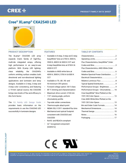
.C R E E .C o m /X L A m pCLD-DS67 Rev 7CCree ® XLamp ® CXA2540 LEDProDuCt DEsCriPtionThe XLamp ® CXA2540 LeD array expands Cree’s family of high‑flux, multi‑die integrated arrays, offering high performance in an easy‑to‑use platform. With XLamp LED lighting‑classreliability,theCXA2540’suniform emitting surface enables both directional and non‑directional lighting applications and luminaire and lamp designs. Available in 2‑step, 3‑step and 4‑step color consistency, and featuring a 19‑mm optical source, the CXA2540 brings new levels of flux and efficacy to this form factor.The CX Family LED Design Guide provides basic information on therequirements to use the CXA2540 LED successfully in luminaire designs.fEAturEs• Available in 4‑step, 3‑step and 2‑stepEasyWhite ® bins at 2700 K, 3000 K, 3500 K, 4000 K & 5000 K CCT and 4‑step EasyWhite bins at 5700 K & 6500 K CCT• Available in ANSI white bins at 4000 K, 5000 K, 5700 K & 6500 K CCT• Available in 70‑, 80‑, 90‑ and 93‑minimum CRI options• Forward voltage option: 36‑V class • 85 °C binning and characterization • Maximum drive current: 2100 mA • 115° viewing angle, uniform chromaticity profile • Top‑side solder connections • Thermocouple attach point• NEMA SSL‑3 2011 standard flux bins • Mechanical and optical footprint consistent with CXA2520 and CXA2530• RoHS‑ and REACh‑compliant • UL ® recognized component (E349212)tAbLE of ContEntsCharacteristics ............................................2Operating Limits ..........................................2Flux Characteristics, EasyWhite ® Order Codes and Bins...........................................3Flux Characteristics, ANSI White Order Codes and Bins ...........................................6Relative Spectral Power Distribution .........7Electrical Characteristics ............................7Relative Luminous Flux ...............................8Typical Spatial Distribution .........................9Performance Groups ‑ Brightness .............9Performance Groups ‑ Chromaticity .......10Cree EasyWhite ® Bins Plotted on the 1931 CIE Color Space ..............................13Cree ANSI White Bins Plotted on the 1931 CIE Color Space ..............................13Bin and Order Code Formats ...................14Mechanical Dimensions ..........................14Thermal Design ........................................15Notes ........................................................16Packaging . (17)ChArACtEristiCsoPErAting LiMitsThe maximum current rating of the CXA2540 is dependent on the case temperature (Tc) when the LED has reached thermal equilibrium under steady‑state operation. The graph shown below assumes that the system design employs good thermal management (thermal interface material and heat sink) and may vary when poor thermal management is employed. Please refer to the Mechanical Drawings section on page 14 for the location of the Tc measurement point.Notes • Cree maintains a tolerance of ±7% on flux and power measurements, ±0.005 on chromaticity (CCx, CCy) measurements and a tolerance of ±2 on CRImeasurements. See the Measurements section (page 16).• Cree XLamp CXA2540 LED order codes specify only a minimum flux bin and not a maximum. Cree may ship reels in flux bins higher than the minimumspecified by the order code without advance notice. Shipments will always adhere to the chromaticity bin restrictions specified by the order code.* Flux values @ 25 °C are calculated and for reference only.fLuX ChArACtEristiCs, EAsyWhitE ® orDEr CoDEs AnD bins (i f = 1100 mA, t J = 85 °C)The following table provides order codes for XLamp CXA2540 LEDs. For a complete description of the order code nomenclature, pleasesee the Bin and Order Code Formats section (page 14).Notes • Cree maintains a tolerance of ±7% on flux and power measurements, ±0.005 on chromaticity (CCx, CCy) measurements and a tolerance of ±2 on CRImeasurements. See the Measurements section (page 16).• Cree XLamp CXA2540 LED order codes specify only a minimum flux bin and not a maximum. Cree may ship reels in flux bins higher than the minimumspecified by the order code without advance notice. Shipments will always adhere to the chromaticity bin restrictions specified by the order code.*Flux values @ 25 °C are calculated and for reference only.fLuX ChArACtEristiCs, EAsyWhitE ® orDEr CoDEs AnD bins (i f = 1100 mA, t J = 85 °C) - ContinuedNotes • Cree maintains a tolerance of ±7% on flux and power measurements, ±0.005 on chromaticity (CCx, CCy) measurements and a tolerance of ±2 on CRImeasurements. See the Measurements section (page 16).• Cree XLamp CXA2540 LED order codes specify only a minimum flux bin and not a maximum. Cree may ship reels in flux bins higher than the minimumspecified by the order code without advance notice. Shipments will always adhere to the chromaticity bin restrictions specified by the order code.*Flux values @ 25 °C are calculated and for reference only.fLuX ChArACtEristiCs, EAsyWhitE ® orDEr CoDEs AnD bins (i f = 1100 mA, t J = 85 °C) - ContinuedNotes • Cree maintains a tolerance of ±7% on flux and power measurements, ±0.005 on chromaticity (CCx, CCy) measurements and a tolerance of ±2 on CRImeasurements. See the Measurements section (page 16).• Cree XLamp CXA2540 LED order codes specify only a minimum flux bin and not a maximum. Cree may ship reels in flux bins higher than the minimumspecified by the order code without advance notice. Shipments will always adhere to the chromaticity bin restrictions specified by the order code.* Flux values @ 25 °C are calculated and for reference only.fLuX ChArACtEristiCs, Ansi WhitE orDEr CoDEs AnD bins (i f = 1100 mA, t J = 85 °C)The following table provides order codes for XLamp CXA2540 LEDs. For a complete description of the order code nomenclature, pleasesee the Bin and Order Code Formats section (page 14).rELAtivE sPECtrAL PoWEr Distribution= 85 °C. The following graph is the result of a series of pulsed measurements at 1100 mA and TJ Array ELECtriCAL ChArACtEristiCsThe following graph is the result of a series of steady‑state measurements.rELAtivE LuMinous fLuXThe relative luminous flux values provided below are the ratio of:• Measurements of CXA2540 at steady‑state operation at the given conditions, divided by= 85 °C.• Flux measured during binning, which is a pulsed measurement at 1100 mA at TJFor example, at steady‑state operation of Tc = 55 °C, I= 1760 mA, the relative luminous flux ratio is 140% in the chart below. A CXA2540F= 1760 mA.LED that measures 4600 lm during binning will deliver 6440 lm (4600 * 1.4) at steady‑state operation of Tc = 55 °C, IFtyPiCAL sPAtiAL DistributionPErforMAnCE grouPs - brightnEss (i f = 1100 mA, t J = 85 °C)XLamp CXA2540 LEDs are tested for luminous flux and placed into one of the following bins.= 85 °C)PErforMAnCE grouPs - ChroMAtiCity (tJXLamp CXA2540 LEDs are tested for chromaticity and placed into one of the regions defined by the following bounding coordinates.PErforMAnCE grouPs - ChroMAtiCity (t= 85 °C) - ContinuedJPErforMAnCE grouPs - ChroMAtiCity (t J= 85 °C) - Continuedbin AnD orDEr CoDE forMAtsBin codes and order codes are configured as follows:order Code bin CodeMEChAniCAL DiMEnsionsDimensions are in mm.Tolerances unless otherwise specified: ±.13x° ± 1°Series = CXA25Chromaticity bin Vf classN0 = 36-V class Internal codeCRI Specification B = 70 min CRI H = 80 min CRI U = 90 min CRI Y = 93 min CRI Flux binPerformance classSeries = CXA25Internal code CRI Specification0 = Standard CRI H = 80 min CRI U = 90 min CRI Y = 93 min CRI Kit codeVf classN0 = 36-V class Performance class1.33.423.85±0.223.85±0.21.33.47.39.53.43.41.31.319.0±0.2 1.15±0.150.55±0.121.0±0.2TcthErMAL DEsignThe CXA family of LED arrays can include over a hundred different LED die inside one package, and thus over a hundred different junction temperatures (T J ). Cree has intentionally removed junction‑temperature‑based operating limits and replaced the commonplace maximum T J calculations with maximum ratings based on forward current (I F ) and case temperature (Tc). No additional calculations are required to ensure the CXA LED is being operated within its designed limits. Please refer to page 2 for the Operating Limit specification.There is no need to calculate for T J inside the package, as the thermal management design process, specifically from solder point (T SP ) to ambient (T a ), remains identical to any other LED component. For more information on thermal management of Cree XLamp LEDs, please refer to the Thermal Management application note . For CXA soldering recommendations and more information on thermal interface materials (TIM) and connection methods, please refer to the Cree XLamp CX Family LEDs soldering and handling document . The CX Family LED Design Guide provides basic information on the requirements to use Cree XLamp CXA LEDs successfully in luminaire designs.To keep the CXA2540 LED at or below the maximum rated Tc, the case to ambient temperature thermal resistance (R_c‑a) must be at or below the maximum R_c‑a value shown on the following graph, depending on the operating environment. The y‑axis in the graph is a base 10 logarithmic scale.As the figure at right shows, the R_c‑a value is the sum of the thermal resistance of the TIM (R_tim) plus the thermal resistance of the heat sink (R_hs).R_j-c Tc R_timR_hs TaR_j-c TcR_c-aTanotEsMeasurementsThe luminous flux, radiant power, chromaticity and CRI measurements in this document are binning specifications only and solely represent product measurements as of the date of shipment. These measurements will change over time based on a number of factors that are not within Cree’s control and are not intended or provided as operational specifications for the products. Calculated values are provided for informational purposes only and are not intended as specifications.Pre-Release Qualification testingPlease read the LED Reliability Overview for details of the qualification process Cree applies to ensure long‑term reliability for XLamp LEDs and details of Cree’s pre‑release qualification testing for XLamp LEDs.Lumen MaintenanceCree now uses standardized IES LM‑80‑08 and TM‑21‑11 methods for collecting long‑term data and extrapolating LED lumen maintenance. For information on the specific LM‑80 data sets available for this LED, refer to the public LM‑80 results document.Please read the Long‑Term Lumen Maintenance application note for more details on Cree’s lumen maintenance testing and forecasting. Please read the Thermal Management application note for details on how thermal design, ambient temperature, and drive current affect the LED junction temperature.rohs ComplianceThe levels of RoHS restricted materials in this product are below the maximum concentration values (also referred to as the threshold limits) permitted for such substances, or are used in an exempted application, in accordance with EU Directive 2011/65/EC (RoHS2), as implemented January 2, 2013. RoHS Declarations for this product can be obtained from your Cree representative or from the Product Documentation sections of .rEACh ComplianceREACh substances of very high concern (SVHCs) information is available for this product. Since the European Chemical Agency (ECHA) has published notice of their intent to frequently revise the SVHC listing for the foreseeable future, please contact a Cree representative to insure you get the most up‑to‑date REACh SVHC Declaration. REACh banned substance information (REACh Article 67) is also available upon request.uL® recognized ComponentLevel 4 enclosure consideration. The LED package or a portion thereof has been investigated as a fire and electrical enclosure per ANSI/ UL 8750.vision AdvisoryWARNING: Do not look at an exposed lamp in operation. Eye injury can result. For more information about LEDs and eye safety, please refer to the LED Eye Safety application note.PACkAgingCree CXA2540 LEDs are packaged in trays of 20. Five trays are sealed in an anti‑static bag and placed inside a carton, for a total of 100 LEDs per carton. Each carton contains 100 LEDs from the same performance bin.Dimensions are in inches.Tolerances: ±.13x° ±1°.375.38PATENT LABEL IS LOCATEDON UNDERSIDE OF COVERLABEL WITH CREE BIN CODE, QUANTITY, LOT #LABEL WITH CREE BIN CODE, QUANTITY, LOT #LABEL WITH CREE BINCODE, QUANTITY, LOT #LABEL WITH CREE BINCODE, QUANTITY, LOT #BAGLABEL WITH CREE BIN CODE, QUANTITY, LOT #。
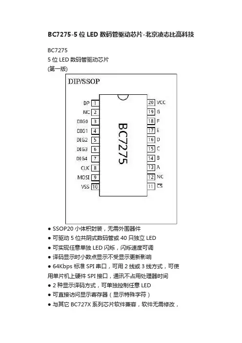
BC7275-5位LED数码管驱动芯片-北京凌志比高科技BC72755位LED数码管驱动芯片(第一版)● SSOP20小体积封装,无需外围器件● 可驱动5位共阴式数码管或40只独立LED● 可实现任意单独LED闪烁,闪烁速度可调● 译码显示时小数点显示不受显示更新影响● 64Kbps 标准SPI串口,可用2线或3线方式,可使用单片机上硬件SPI接口,通讯不占用处理器时间● 2种显示译码方式,可单独控制任意LED● 可直接访问显示寄存器(显示特殊字符)● 与其它BC727X系列芯片软件兼容,软件无需修改,即可用于其它BC727X芯片摘要BC7275具有5位数码管显示管理功能。
因为支持段寻址,可以独立地控制每一个显示段,故也可用于最多40个独立的LED驱动。
BC7275支持闪烁显示功能,且闪烁速度可调,可以独立控制每一段的闪烁,在使用独立的LED指示灯时,非常有用。
BC7275内部提供译码功能,用户可以直接向译码寄存器写入数值,而得到相应数字显示。
译码显示时,该位的小数点显示不受影响,用户只需更新显示数据,而无需考虑小数点的问题,尤其对于将小数点用作单独指示灯的用户,使用非常简便。
同时,也支持直接写入显示寄存器,可以完成一些特殊字符的显示。
BC7275采用串行接口,可以直接与标准SPI接口连接,通讯速率可达64Kbps,用户可以充分利用微处理器上硬件SPI接口资源,当使用中断方式时,可使显示部分的通讯几乎不占用主程序时间。
BC7275的SPI接口可以接为2线或三线方式。
三线方式时,可以通过CS 片选信号,在一个SPI总线上使用多个器件,而在MCU I/O口资源紧张时,片选CS线可以直接接地,其内部独特的SPI口计时复位逻辑可以使得即便没有片选信号的接口清零功能,也可以保障通讯不会出错。
极限参数:(注:超出所列范围有可能造成器件永久损坏)储存温度-65至+150°C工作温度-40至+85°C任意脚对地电压-0.5至6.0V电特性:(除特别说明外,T A=25°C, Vcc=5.0V)参数最小值典型值最大值单位备注电源电压 2.7 5.0 5.5V工作电流 4.9mA无LED负载时输入低电平 1.4V输入高电平 3.7V当Vcc=3V时,为1.9V输出低电平0.1V输出高电平 4.4V显示扫描周期15mS引脚说明:名称序号说明DP1小数点段驱动DIG0-DIG43,4,5,6,7位驱动,分别接数码管的共阳端CLK8SPI串行输入时钟端,最大时钟频率64KHz,空闲时高电平MOSI9SPI口数据输入端,接MCU的SPI口数据输出端GND10接地端CS11片选端,低电平有效A段-G段段驱动A-G13,14,15,16,17,18,19VCC20正电源端,电压范围2.7-5.5V内部寄存器BC7275内部具有18个寄存器,包括5个显示寄存器,以及13个特殊寄存器。
4位数码管驱动芯片4位数码管驱动芯片是一种集成电路芯片,用于控制和驱动四位数码管显示器。
它通常包含多个功能模块,如扫描驱动、段选驱动、亮度调节等,以完成对数码管显示的控制。
4位数码管驱动芯片的核心功能是实现对4个数码管的控制和驱动。
它往往具备以下特点和功能:1. 扫描驱动:可以通过扫描方式实现对多位数码管的驱动。
通过扫描驱动的方式,可以轮流控制每个数码管的选通,从而实现多位数码管的显示。
2. 段选驱动:对于每个数码管的每个段(例如A、B、C、D、E、F、G等),能够通过相应控制信号的输入,实现对特定段的亮灭控制。
这样可以根据需要显示不同的数字、字母或符号。
3. 亮度调节:可以通过外部控制信号,调节数码管的亮度。
通常使用PWM(脉冲宽度调制)技术来实现亮度的调节。
4. 时钟控制:数码管的刷新速度需要一个时钟信号来驱动,4位数码管驱动芯片可以内部产生相应的时钟信号,也可以通过外部输入时钟信号来控制。
5. 输入控制:芯片通常提供多个输入引脚,用以接收外部控制信号,实现对数码管的控制和显示。
6. 常用功能和显示模式支持:该芯片通常支持常用的显示模式,例如静态显示模式、动态扫描显示模式、按键扫描模式等,以满足不同场景下的需求。
7. 多数字管级联:该芯片通常支持多位数码管的级联。
通过级联,可以按照需要来扩展显示位数,并通过芯片的控制实现对多位数码管的统一控制。
总之,4位数码管驱动芯片是一种专门用于控制和驱动4位数码管显示器的集成电路芯片。
它具备扫描驱动、段选驱动、亮度调节、时钟控制以及常用功能和显示模式支持等功能,可以满足各种场景下的数码管显示需求。
4位半数码管驱动ic4位半数码管驱动IC是一种常用的电子元件,用来控制和驱动4位数码管的显示。
它在电子制造业中扮演着重要的角色,广泛应用于各种计时器、测量仪器、电子钟表等设备中。
本文将从工作原理、特点、应用领域等方面,综合介绍4位半数码管驱动IC的相关知识。
首先,我们来了解一下4位半数码管驱动IC的工作原理。
它基于集成电路技术,内部集成了多个逻辑门、锁存器、驱动器等功能模块。
通过外部控制电路的输入信号,可以实现对数码管的控制。
具体而言,它可以根据输入的数据信号,通过逻辑运算和锁存操作,将对应的数字码输出到数码管的对应位置上,实现数字的显示。
4位半数码管驱动IC具有很多特点。
首先,它体积小,功耗低,结构紧凑,便于集成到各种电子设备中。
其次,它具有较高的工作稳定性和可靠性,能够长时间保持数码管的正常显示。
另外,它还具有广泛的工作电压范围和电流驱动能力,可以适应不同的工作环境和需求。
4位半数码管驱动IC在各个领域具有广泛的应用。
在计时器方面,它可以用于电子钟表、秒表、倒计时器等设备中,实现时间的精确显示和计时功能。
在测量仪器方面,它可以被用作数字电压表、电流表、频率计等设备中,方便用户进行数据的读取和显示。
此外,它还可以应用于数码温度计、数码计数器等各种仪器设备中。
对于DIY爱好者和电子爱好者来说,4位半数码管驱动IC也是非常有用的。
通过自己搭建电路,可以将它用于各种个性化的小制作中,如数字时钟、计数器等,达到独特的效果。
总而言之,4位半数码管驱动IC是一种非常重要的电子元件,在电子制造业和各种设备中拥有广泛的应用。
它的工作原理基于集成电路技术,具有体积小、功耗低、工作稳定等特点。
无论是在计时器、测量仪器,还是在个人制作方面,它都能发挥重要的作用。
希望通过本文的介绍,读者能够更加了解和认识这一独特的IC元件,为电子制作和应用提供指导和参考。
数码管驱动芯片有哪些数码管是一种显示设备,它是由多个发光二极管组成的。
为了驱动数码管的显示,需要使用特定的驱动芯片。
下面是一些常见的数码管驱动芯片:1. TM1637:TM1637是一种常用的4位数码管驱动芯片,适用于控制共阳或共阴数码管。
它具有简单的接口和丰富的功能,可以轻松实现数字、字母、符号的显示和控制。
2. TM1650:TM1650是一种集成了键盘扫描和数码管驱动功能的芯片。
它可以同时驱动4位数码管,并且具有内置的键盘扫描功能,可直接与开关矩阵连接,实现灵活的控制。
3. MAX7219:MAX7219是一种广泛使用的8位数码管驱动器,具有独特的串行接口。
它可以同时驱动8位共阳或共阴数码管,并且可以级联多个芯片,实现更多数码管的显示。
4. HT1621:HT1621是一种针对液晶数码管设计的驱动芯片,可以同时驱动4位数码管,同时支持多种显示模式和字符设置。
它具有低功耗特性和简单易用的接口。
5. CD4543:CD4543是一种BCD-7段数码管驱动芯片,适用于显示0-9数字和部分字母。
它具有直接BCD码输入和简单的复位功能。
6. CD4511:CD4511是一种BCD-7段数码管驱动芯片,适用于显示0-9数字和部分字母。
它具有多种输入模式和BCD码转换功能。
7. HT1622:HT1622是一种驱动静态和多功能数码管显示的专用控制器,兼容于HT1621。
它具有低功耗和扫描速度快的特点。
8. MBI5168:MBI5168是一种高亮度LED数码管驱动芯片,适用于控制共阳数码管。
它具有高驱动电流能力和优秀的亮度调节范围。
除了这些常见的数码管驱动芯片外,还有许多其他型号和品牌的芯片可供选择。
根据不同的应用场景和需求,选择合适的数码管驱动芯片非常重要。
led驱动芯片大全LED驱动芯片是指用于控制和驱动LED灯的电子元件。
随着LED技术的不断发展,LED驱动芯片也得到了广泛的应用。
下面将介绍一些常见的LED驱动芯片。
1. LM317: 这是一款常见的线性稳压器芯片,可用于驱动小功率的LED灯。
它具有良好的稳定性和低噪音特性。
2. PT4115: 这是一款高效的恒流LED驱动芯片,可用于驱动中功率的LED灯。
它具有宽输入电压范围、高达97%的转换效率和短路保护功能。
3. XL6009: 这是一款升压型DC-DC转换芯片,可用于驱动高亮度LED灯。
它具有宽输入电压范围、高达94%的转换效率和过流保护功能。
4. WS2812: 这是一款数字式LED驱动芯片,可用于驱动彩色LED灯。
它具有内置控制电路和存储器,能够实现多种色彩和灯效的变换。
5. TLC5940: 这是一款多路PWM输出型LED驱动芯片,可用于驱动多个LED灯。
它具有16路独立控制的PWM输出和电流控制功能。
6. AL9910: 这是一款高精度电流调节型LED驱动芯片,可用于驱动大功率LED灯。
它具有高达97%的转换效率和电流模式调光功能。
7. LT3754: 这是一款降压型DC-DC转换和恒流LED驱动芯片,可用于驱动多个串联LED灯。
它具有宽输入电压范围和高达97%的转换效率。
8. MAX16822: 这是一款高效、同步型的恒流LED驱动芯片,可用于驱动大功率LED灯。
它具有高达97%的转换效率和短路保护功能。
9. HV9961: 这是一款高压恒流LED驱动芯片,可用于驱动串联LED灯。
它具有宽输入电压范围、高达96%的转换效率和短路保护功能。
10. ILD600: 这是一款恒流LED驱动芯片,可用于驱动小功率LED灯。
它具有宽输入电压范围、过温保护和短路保护功能。
以上是一些常见的LED驱动芯片,它们具有不同的特点和适用范围。
在选择LED驱动芯片时,需要根据LED灯的功率和特性来进行选择,并注意选用符合安全标准的产品。
4位半数码管驱动ic
摘要:
1.半数码管驱动ic的基本概念
2.4位半数码管驱动ic的特点
3.4位半数码管驱动ic的应用领域
4.4位半数码管驱动ic的市场前景
正文:
半数码管驱动ic是一种专门用于驱动数码管的集成电路,它能将数字信号转换为驱动数码管所需的电信号,从而实现数码管的显示。
在众多半数码管驱动ic中,4位半数码管驱动ic以其独特的优势得到了广泛应用。
首先,4位半数码管驱动ic的特点在于其具有较高的集成度和较低的功耗。
它能同时驱动4位共阴极数码管,减少了外部元件的数量,简化了电路设计。
此外,由于采用了先进的工艺技术,4位半数码管驱动ic的功耗大大降低,从而延长了设备的续航时间。
其次,4位半数码管驱动ic具有较高的兼容性和稳定性。
它可以与各种类型的数码管相匹配,从而方便了用户的选择和使用。
同时,4位半数码管驱动ic具有较强的抗干扰能力,能在恶劣的电磁环境中稳定工作,保证了显示效果的可靠性。
在应用领域方面,4位半数码管驱动ic广泛应用于各种电子设备中,如计时器、计数器、显示屏等。
通过使用4位半数码管驱动ic,这些设备可以实现高亮度、低功耗、长寿命的显示效果,提高了设备的性能和用户体验。
总之,随着科技的不断进步和市场需求的日益增长,4位半数码管驱动ic 的市场前景十分广阔。
VK16K33是一种带按键扫描接口的数码管或点阵LED驱动控制专用芯片概述:VK16K33是一种带按键扫描接口的数码管或点阵LED驱动控制专用芯片,内部集成有数据锁存器、键盘扫描、LED 驱动模块等电路。
数据通过I2C通讯接口与MCU通信。
SEG脚接LED阳极,GRID脚接LED阴极,可支持16SEGx8GRID的点阵LED显示面板。
最大支持13×3的按键。
内置上电复位电路,整体闪烁频率可设置,可通过命令进入待机模式,采用SOP20/SOP24/SOP28三种封装形式。
特点:•工作电压 3.0-5.5V•内置 RC振荡器•陈锐鸿:188.2466.2436• QQ:361.888.5898•最大16个SEG脚,8个GRID脚 (封装不同SEG脚数量不同)• SEG脚只能接LED阳极,GRID脚只能接LED阴极• I2C通讯接口,I2C从机地址可通过IO脚选择• 16级整体亮度可调•最大13×3的按键扫描按键显示复用需硬件电路配合支持组合键需要电路配合)•读/写地址自动加1•内置显示RAM为16x8位•内置上电复位电路•整体闪烁频率可设置•通过命令进入待机模式•驱动电流大,适合高亮显示场合•封装:SOP28(300mil)(18.00mm×7.50mm PP=1.27mm)SOP24(300mil)(15.40mm×7.50mm PP=1.27mm)SOP20(300mil)(12.80mm×7.50mm PP=1.27mm)——————————————————————————————————内存映射的LED控制器及驱动器VK1628---通讯接口:STb/CLK/DIO 电源电压:5V(4.5~5.5V) 驱动点阵:70/52共阴驱动:10段7位/13段4位共阳驱动:7段10位按键:10x2 封装SOP28VK1629---通讯接口:STb/CLK/DIN/DOUT 电源电压:5V(4.5~5.5V) 驱动点阵:128共阴驱动:16段8位共阳驱动:8段16位按键:8x4 封装QFP44VK1629A---通讯接口:STb/CLK/DIO 电源电压:5V(4.5~5.5V) 驱动点阵:128共阴驱动:16段8位共阳驱动:8段16位按键:--- 封装SOP32VK1629B---通讯接口:STb/CLK/DIO 电源电压:5V(4.5~5.5V) 驱动点阵:112共阴驱动:14段8位共阳驱动:8段14位按键:8x2 封装SOP32VK1629C---通讯接口:STb/CLK/DIO 电源电压:5V(4.5~5.5V) 驱动点阵:120共阴驱动:15段8位共阳驱动:8段15位按键:8x1 封装SOP32VK1629D---通讯接口:STb/CLK/DIO 电源电压:5V(4.5~5.5V) 驱动点阵:96共阴驱动:12段8位共阳驱动:8段12位按键:8x4 封装SOP32VK1640---通讯接口: CLK/DIN 电源电压:5V(4.5~5.5V) 驱动点阵:128共阴驱动:8段16位共阳驱动:16段8位按键:--- 封装SOP28VK1640A---通讯接口: CLK/DIN 电源电压:5V(4.5~5.5V) 驱动点阵:128共阴驱动:8段16位共阳驱动:16段8位按键:--- 封装SSOP28VK1640B---通讯接口: CLK/DIN 电源电压:5V(4.5~5.5V) 驱动点阵:96 共阴驱动:8段12位共阳驱动:12段8位按键:--- 封装SSOP24VK1650---通讯接口: SCL/SDA 电源电压:5V(3.0~5.5V)共阴驱动:8段4位共阳驱动:4段8位按键:7x4 封装SOP16/DIP16VK1651---通讯接口: SCL/SDA 电源电压:5V(3.0~5.5V)共阴驱动:7段4位共阳驱动:4段7位按键:7x1 封装SOP16/DIP16VK1616---通讯接口: 三线串行电源电压:5V(3.0~5.5V)显示模式:7段4位按键:7x1 封装SOP16/DIP16VK1668---通讯接口:STb/CLK/DIO 电源电压:5V(4.5~5.5V) 驱动点阵:70/52共阴驱动:10段7位/13段4位共阳驱动:7段10位按键:10x2 封装SOP24VK6932---通讯接口:STb/CLK/DIN 电源电压:5V(4.5~5.5V) 驱动点阵:128共阴驱动:8段16位17.5/140mA 共阳驱动:16段8位按键:--- 封装SOP32VK16K33A/B/C---通讯接口:SCL/SDA 电源电压:5V(4.5V~5.5V)驱动点阵:128/96/64共阴驱动:16段8位/12段8位/8段8位共阳驱动:8段16位/8段12位/8段8位按键:13x3 10x3 8x3封装SOP20/SOP24/SOP28VK1618---带键盘扫描接口的LED驱动控制专用电路,内部集成有MCU数字接口、数据锁存器、键盘扫描等电路共阴驱动:5段7位/6段6位/7段5位/8段4位共阳驱动:7段5位/6段6位/5段7位/4段8位按键:5x1 封装SOP18/DIP18VK1S68C---LED驅動IC 10x7/13x4段位10段7位/11段6位共阴10x2按键,封装SSOP24VK1Q68D---LED驅動IC 10x7/13x4段位10段7位/11段6位共阴10x2按键,封装QFP24VK1S38A---LED驱动IC 8段×8位封装SSOP24VK1638--- LED驱动IC 共阴10段8位共阳8段10位封装SOP32 ——————————————————————————————————LCD/LED液晶控制器及驱动器系列芯片简介如下:RAM映射LCD控制器和驱动器系列:VK1024B 2.4~5.2V SEG*COM:6*4、6*3、6*2 偏置电压1/2 1/3 S0P-16VK1056B 2.4~5.2V SEG*COM:14*4、14*3/14*2偏置电压1/2 1/3 SOP/SSOP24VK1072B 2.4~5.2V SEG*COM:18*4、18*3、18*2偏置电压1/2 1/3 SOP28VK1072C 2.4~5.2V SEG*COM:18*4、18*3、18*2偏置电压1/2 1/3 SOP28VK1072D 2.4~5.2V SEG*COM:18*4、18*3、18*2偏置电压1/2 1/3 SSOP28 VK1088B 2.4~5.2V SEG*COM:22*4、22*3、22*2 偏置电压1/2 1/3 QFN32(4*4) VK0192 2.4~5.2V 24seg*8com 偏置电压1/4 LQFP-44VK0256 2.4~5.2V 32seg*8com 偏置电压1/4 QFP-64VK0256B 2.4~5.2V 32seg*8com 偏置电压1/4 LQFP-64VK0256C 2.4~5.2V 32seg*8com 偏置电压1/4 LQFP-52VK1621 2.4~5.2V SEG*COM:32*4、32*3、32*2偏置电压1/2 1/3 LQFP44/48/SSOP48/SKY28/DICE裸片VK1622 2.4~5.5V 32seg*8com偏置电压1/4 LQFP44/48/52/64/QFP64/DICE裸片VK1623 2.4~5.2V 48seg*8com偏置电压1/4 LQFP-100/QFP-100/DICE裸片VK1625 2.4~5.2V 64seg*8com偏置电压1/4 LQFP-100/QFP-100/DICE 裸片VK1626 2.4~5.2V 48seg*16com偏置电压1/5 LQFP-100/QFP-100/DICE 裸片——————————————————————————————————高抗干扰LCD液晶控制器及驱动系列:VK2C21A 2.4~5.5V 20seg*4com 16*8 偏置电压1/3 1/4 I2C通讯接口 SOP-28VK2C21B 2.4~5.5V 16seg*4com 12*8 偏置电压1/3 1/4 I2C通讯接口 SOP-24VK2C21C 2.4~5.5V 12seg*4com 8*8 偏置电压1/3 1/4 I2C通讯接口 SOP-20VK2C21D 2.4~5.5V 8seg*4com 4*8 偏置电压1/3 1/4 I2C通讯接口 SOP-16VK2C22A 2.4~5.5V 44seg*4com 偏置电压1/2 1/3 I2C通讯接口 LQFP-52VK2C22B 2.4~5.5V 40seg*4com 偏置电压1/2 1/3 I2C通讯接口 LQFP-48VK2C23A 2.4~5.5V 56seg*4com 52*8 偏置电压1/3 1/4 I2C通讯接口 LQFP-64VK2C23B 2.4~5.5V 36seg*8com 偏置电压1/31/4 I2C通讯接口 LQFP-48VK2C24 2.4~5.5V 72seg*4com 68*8 60*16 偏置电压1/31/4 1/5 I2C通讯接口 LQFP-80超低功耗LCD液晶控制器及驱动系列:VKL060 2.5~5.5V 15seg*4com 偏置电压1/21/3 I2C通讯接口SSOP-24VKL128 2.5~5.5V 32seg*4com 偏置电压1/21/3 I2C通讯接口LQFP-44VKL144A 2.5~5.5V 36seg*4com 偏置电压1/21/3 I2C通讯接口TSSOP-48VKL144B 2.5~5.5V 36seg*4com 偏置电压1/21/3 I2C通讯接口QFN48L (6MM*6MM)静态显示LCD液晶控制器及驱动系列:VKS118 2.4~5.2V 118seg*2com 偏置电压 -- 4线通讯接口LQFP-128VKS232 2.4~5.2V 116seg*2com 偏置电压1/1 1/2 4线通讯接口LQFP-128 ——————————————————————————————————触摸触控IC系列简介如下:标准触控IC-电池供电系列:VKD223EB --- 工作电压/电流:2.0V-5.5V/5uA-3V 感应通道数:1 通讯接口最长响应时间快速模式60mS,低功耗模式220ms 封装:SOT23-6VKD223B --- 工作电压/电流:2.0V-5.5V/5uA-3V 感应通道数:1通讯接口最长响应时间快速模式60mS,低功耗模式220ms 封装:SOT23-6VKD233DB ---工作电压/电流:2.4V-5.5V/2.5uA-3V 1感应按键封装:SOT23-6 通讯接口:直接输出,锁存(toggle)输出低功耗模式电流2.5uA-3VVKD233DH ---工作电压/电流:2.4V-5.5V/2.5uA-3V 1感应按键封装:SOT23-6 通讯接口:直接输出,锁存(toggle)输出有效键最长时间检测16SVKD233DS ---工作电压/电流:2.4V-5.5V/2.5uA-3V 1感应按键封装:DFN6通讯接口:直接输出,锁存(toggle)输出低功耗模式电流2.5uA-3VVKD233DR ---工作电压/电流:2.4V-5.5V/1.5uA-3V 1感应按键封装:DFN6 通讯接口:直接输出,锁存(toggle)输出低功耗模式电流1.5uA-3VVKD233DG --- 工作电压/电流:2.4V-5.5V/2.5uA-3V 1感应按键封装:DFN6 通讯接口:直接输出,锁存(toggle)输出低功耗模式电流2.5uA-3VVKD233DQ --- 工作电压/电流:2.4V-5.5V/5uA-3V 1感应按键封装:SOT23-6通讯接口:直接输出,锁存(toggle)输出低功耗模式电流5uA-3VVKD233DM --- 工作电压/电流:2.4V-5.5V/5uA-3V 1感应按键封装:SOT23-6 (开漏输出)通讯接口:开漏输出,锁存(toggle)输出低功耗模式电流5uA-3VVKD232C--- 工作电压/电流:2.4V-5.5V/2.5uA-3V 感应通道数:2 封装:SOT23-6通讯接口:直接输出,低电平有效固定为多键输出模式,內建稳压电路——————————————————————————————————MTP触摸IC——VK36N系列抗电源辐射及手机干扰:VK3601L --- 工作电压/电流:2.4V-5.5V/4UA-3V3 感应通道数:1 1对1直接输出待机电流小,抗电源及手机干扰,可通过CAP调节灵敏封装:SOT23-6VK36N1D --- 工作电压/电流:2.2V-5.5V/7UA-3V3 感应通道数:1 1对1直接输出触摸积水仍可操作,抗电源及手机干扰,可通过CAP调节灵敏封装:SOT23-6VK36N2P --- 工作电压/电流:2.2V-5.5V/7UA-3V3 感应通道数:2 脉冲输出触摸积水仍可操作,抗电源及手机干扰,可通过CAP调节灵敏封装:SOT23-6VK3602XS ---工作电压/电流:2.4V-5.5V/60UA-3V 感应通道数:2 2对2锁存输出低功耗模式电流8uA-3V,抗电源辐射干扰,宽供电电压封装:SOP8VK3602K --- 工作电压/电流:2.4V-5.5V/60UA-3V 感应通道数:2 2对2直接输出低功耗模式电流8uA-3V,抗电源辐射干扰,宽供电电压封装:SOP8VK36N2D --- 工作电压/电流:2.2V-5.5V/7UA-3V3 感应通道数:2 1对1直接输出触摸积水仍可操作,抗电源及手机干扰,可通过CAP调节灵敏封装:SOP8VK36N3BT ---工作电压/电流:2.2V-5.5V/7UA-3V3 感应通道数:3 BCD码锁存输出触摸积水仍可操作,抗电源及手机干扰,可通过CAP调节灵敏封装:SOP8VK36N3BD ---工作电压/电流:2.2V-5.5V/7UA-3V3 感应通道数:3 BCD码直接输出触摸积水仍可操作,抗电源及手机干扰,可通过CAP调节灵敏封装:SOP8VK36N3BO ---工作电压/电流:2.2V-5.5V/7UA-3V3 感应通道数:3 BCD码开漏输出触摸积水仍可操作,抗电源及手机干扰封装:SOP8/DFN8(超小超薄体积)VK36N3D --- 工作电压/电流:2.2V-5.5V/7UA-3V3 感应通道数:3 1对1直接输出触摸积水仍可操作,抗电源及手机干扰封装:SOP16/DFN16(超小超薄体积)VK36N4B ---工作电压/电流:2.2V-5.5V/7UA-3V3 感应通道数:4 BCD输出触摸积水仍可操作,抗电源及手机干扰封装:SOP16/DFN16(超小超薄体积)VK36N4I---工作电压/电流:2.2V-5.5V/7UA-3V3 感应通道数:4 I2C输出触摸积水仍可操作,抗电源及手机干扰封装:SOP16/DFN16(超小超薄体积)VK36N5D ---工作电压/电流:2.2V-5.5V/7UA-3V3 感应通道数:5 1对1直接输出触摸积水仍可操作,抗电源及手机干扰封装:SOP16/DFN16(超小超薄体积)VK36N5B ---工作电压/电流:2.2V-5.5V/7UA-3V3 感应通道数:5 BCD输出触摸积水仍可操作,抗电源及手机干扰封装:SOP16/DFN16(超小超薄体积)VK36N5I ---工作电压/电流:2.2V-5.5V/7UA-3V3 感应通道数:5 I2C输出触摸积水仍可操作,抗电源及手机干扰封装:SOP16/DFN16(超小超薄体积)VK36N6D --- 工作电压/电流:2.2V-5.5V/7UA-3V3 感应通道数:6 1对1直接输出触摸积水仍可操作,抗电源及手机干扰封装:SOP16/DFN16(超小超薄体积)VK36N6B ---工作电压/电流:2.2V-5.5V/7UA-3V3 感应通道数:6 BCD输出触摸积水仍可操作,抗电源及手机干扰封装:SOP16/DFN16(超小超薄体积)VK36N6I ---工作电压/电流:2.2V-5.5V/7UA-3V3 感应通道数:6 I2C输出触摸积水仍可操作,抗电源及手机干扰封装:SOP16/DFN16(超小超薄体积)VK36N7B ---工作电压/电流:2.2V-5.5V/7UA-3V3 感应通道数:7 BCD输出触摸积水仍可操作,抗电源及手机干扰封装:SOP16/DFN16(超小超薄体积)VK36N7I ---工作电压/电流:2.2V-5.5V/7UA-3V3 感应通道数:7 I2C输出触摸积水仍可操作,抗电源及手机干扰封装:SOP16/DFN16(超小超薄体积)VK36N8B ---工作电压/电流:2.2V-5.5V/7UA-3V3 感应通道数:8 BCD输出触摸积水仍可操作,抗电源及手机干扰封装:SOP16/DFN16(超小超薄体积)VK36N8I ---工作电压/电流:2.2V-5.5V/7UA-3V3 感应通道数:8 I2C输出触摸积水仍可操作,抗电源及手机干扰封装:SOP16/DFN16(超小超薄体积)VK36N9I ---工作电压/电流:2.2V-5.5V/7UA-3V3 感应通道数:9 I2C输出触摸积水仍可操作,抗电源及手机干扰封装:SOP16/DFN16(超小超薄体积)VK36N10I ---工作电压/电流:2.2V-5.5V/7UA-3V3 感应通道数:10 I2C输出触摸积水仍可操作,抗电源及手机干扰封装:SOP16/DFN16(超小超薄体积)——————————————————————————————————1-8点高灵敏度液体水位检测IC——VK36W系列VK36W1D ---工作电压/电流:2.2V-5.5V/10UA-3V3 1对1直接输出水位检测通道:1可用于不同壁厚和不同水质水位检测,抗电源/手机干扰封装:SOT23-6备注:1. 开漏输出低电平有效2、适合需要抗干扰性好的产品应用VK36W2D ---工作电压/电流:2.2V-5.5V/10UA-3V3 1对1直接输出水位检测通道:2可用于不同壁厚和不同水质水位检测,抗电源/手机干扰封装:SOP8备注:1. 1对1直接输出 2、输出模式/输出电平可通过IO选择VK36W4D ---工作电压/电流:2.2V-5.5V/10UA-3V3 1对1直接输出水位检测通道:4可用于不同壁厚和不同水质水位检测,抗电源/手机干扰封装:SOP16/DFN16 备注:1. 1对1直接输出 2、输出模式/输出电平可通过IO选择VK36W6D ---工作电压/电流:2.2V-5.5V/10UA-3V3 1对1直接输出水位检测通道:6可用于不同壁厚和不同水质水位检测,抗电源/手机干扰封装:SOP16/DFN16 备注:1. 1对1直接输出2、输出模式/输出电平可通过IO选择VK36W8I ---工作电压/电流:2.2V-5.5V/10UA-3V3 I2C输出水位检测通道:8可用于不同壁厚和不同水质水位检测,抗电源/手机干扰封装:SOP16/DFN16。