Circuit Envelope Simulation
- 格式:ppt
- 大小:495.50 KB
- 文档页数:14
10Helpful Hints for using the HP Advanced Design SystemHINTSCONTENTSLearning to “Drive” Using the Keyboard (3)Using Templates or Copying Examples for More Efficient Simulation Set-up andData Display (4)Saving Mouse Clicks when Opening Projects (5)Renaming Ports on Schematics before Generating Subcircuits (6)Enabling Easy Display of Data (7)Efficiently Calculate Circuit Envelope Simulation Data (8)Using Short Cuts when Generating Schematics (9)Replacing MDS Wire Labels and Series IV Test Points with Node Names (10)Using New and Improved Data Display Capabilities (11)Managing Projects (12)Learning to “Drive” Using the KeyboardHINT1When you first learn to “drive”a software program, it is usu-ally easiest to use the mouse.As you become more of an expert user, however, it can often be faster to use the key-board to execute commands.Also, heavy software users who rely too much on mouse opera-tions run the risk of developing repetitive strain injuries.The HP Advanced Design Sys-tem has many built-in hot keys (Alt+f , for example, opens the File menu), and you can cus-tomize hot keys to perform operations that you use fre-quently .In the Options menu of the Main window or of a design window , the commandMenu/Toolbar Configurationopens the Customization dia-log box where you can custom-ize both hot keys and the tool bar configuration. In the Main window , you can customize Main window operations; in a design window , you can cus-tomize hot keys for that type of design (schematic and layout are set independently).Hot key suggestions for editing schematics:f for View All d for Redraw View z for Zoom Area 2 for Zoom Out x2e for Edit Component Param.t for Draw (insert) Text w for Component Wire (draw-ing wires between components)m for Move & Disconnect (inmost cases, this is preferable to the Move command, which causes wires to remain con-nected)ctrl+o for View/ Push Into Hier-archyUse F7 to launch simulations,and the escape key to termi-nate commands.F5 moves component text.After moving a component, it remains selected. To deselect it, just click on a blank spot in the schematic.Figure 1.Setting Schematic HotKeysall of the *.dds files in the example project are dis-played.8.Select the example.dds fileyou want to display , and open it.9.Copy and paste desiredplots, equations, etc., from the example.dds file into your data display window .Openingan Example Schematic from within a Project1.In a schematic window ,choose Window > Schematic .2.In the new Schematic win-dow , choose File > Open .3.In the Open Design dialogbox, click Browse .4.Traverse the directory treeto find the desired project and design.3.If you know the exampleproject path, you can type it in and skip the remain-ing steps. If you do not, go to the Main window and choose File >Copy Project .4.On the From Project: line,click on the Examples but-ton and then the Browse button.5.Traverse the examplesdirectory tree until the project that contains the data display that you want is entered in the Selection field of the Copy From File Browse dialog box.6.Clear the Filter field of theOpen data display dialog box.7.Highlight the exampleselection in the Copy From File Browse dialog box, and paste it into the Filter field of the Open data display dialog box. Append the suf-fix *.dds in this field, andWhen you set up a simulation, never start from scratch if you can avoid it.Often the fastest way to set up a simu-lation is to copy a schematic from an example or from another project.You can use any saved schematic or data display window as a template,including those in the program’s examples directory .You can also open a separate schematic window and display a schematic from an example or a different project.Viewing a Data DisplayUse the following steps to view a data display from an example file when you already have a data display open:1.In a Data Display window , chooseFile >New and open a new data dis-play window .2.In the new data display window ,choose File > Open.3.Define the directory, then click Filter todisplay the projects in4.Select a project,File > Copy Project7.Keep hierarchyin copy.8.Copy the project.6.Enter a name,5.To have the copy placed in a different directory than the original, click the desireddirectory type and Browse .Unless you specify a different directory , the copy is placed in the same directory as the project that was copied.2.Click Browse.1.Click the desired directory type.Figure 1.The Basics of Copying FilesHINT2Using Templates or Copying Examples for More EfficientSimulation Set-up and Data DisplaySaving Mouse Clicks when Opening ProjectsHINT3You can have the programreopen design windows for you when you reopen a project:1.In the Main Preferencesdialog box, select SaveProject Status on Exit(default is unselected).2.When you change projectsor exit the program, leave the design window(s) open that you want to see when you reopen the project.The next time you open the project, the last designs that where open will open automat-ically , saving you several mouse clicks.Figure 1.Saving Open DesignWindowsSelect this OptionHINT4Renaming Ports on Schematics before Generating SubcircuitsFigure 1.Schematic with Named PortsFigure 2. SymbolDesigners often use subcircuits to keep simulation set-ups easy to read. When you gener-ate a symbol for a subcircuit,you must place a port on the schematic at any input or out-put point, and the program provides the ports with default names (P1, P2, and so on).If you change the default names (to something moredescriptive such as Input, Out-put, Vplus, Vminus, for exam-ple), the names you give the ports appear on the subcircuit symbol when it is created. You may have to move the names on the symbol view so they do not overlap, but having the names on the symbol make it easier to correctly wire the sub-circuit into a higher-level cir-cuit.Enabling Easy Display of Data HINT5Using the shortest possiblevariable names in a data dis-play makes it easier to displaydata when you want to changedatasets. For example, after aharmonic balance simulation,instead of entering the equa-tion:Spectrum=dBm(SmampHBtest.HB1.HB1.HB.Vout)just enter the equation:Spectrum=dBm(Vout)This way, to display a spectrumusing a different dataset, allyou have to do is change thedataset name in the defaultdataset window. Using com-plete variable names (as in thefirst equation above)is neces-sary when you want to displaythe results of two differentsimulations simultaneously.ing Short Variable NamesHINT6Efficiently CalculateCircuit Envelope Simulation DataFigure ing an IntermediateVariableWhen doing calculations with or displaying Circuit Envelope data, calculations are much faster if you define an interme-diate variable. For example, if you simulate an amplifier with a digitally-modulated input signal in order to calculate the adjacent-channel power ratio or plot a trajectory diagram,you must extract the resulting fundamental frequencycomponent, which is a function of time. For example, to see the resulting output spectrum near the fundamental fre-quency ,use the following equations:Voutfund=Vout[1]Spectrum=dBm(0.5*fs(Voutfund,,,,,"Kaiser”))Trajectory=vs(imag(Voutfund),real(Voutfund))This will lead to faster data display calculations than using Vout[1] directly in all of the expressions.HINT Using Short Cuts whenGenerating Schematics7When you create a schematic,there are a couple techniquesthat can help speed things up:1.Copy components that youhave already placed on theschematic, rather thanplacing new ones (usingthe menus or palettes)each time.2.Enter component namesin the Component Historywindow. For example, typeR for resistor, and pressEnter. Then place the com-ponent in the schematic.You must type in the exactname of the component youwant; remember that ADSis case sensitive.3.Because the ComponentHistory window keeps alist of the components youplace in the schematic(after initially opening thewindow), if you see that aparticular component isClick here to display the drop-down list already in the schematic,you can click thedown-arrow next to theComponent History win-dow, select the desiredcomponent, and insert thepart in the schematic.ponent History Window with List of Placed ComponentsHINT8Replacing MDS Wire Labels and Series IV Test Points with Node NamesFigure 1.IF Output Schematic with NodeNamesWhere MDS uses wire labels to identify node voltages that are to be output to a dataset, and Series IV uses test points to identify node voltages to be used in calculations, theHP Advanced Design System uses node names.To insert a node name:1.Either select the “nodename” icon, which looks like a resistor with a rect-angle below it, or choose the command,Component >Node Name .2.Type in the name youwould like to attach to a particular node.3.Select a component pin.When placing a node name, you must select a component pin. In the HP Advanced Design Sys-tem 1.0, you cannot place node names on a wire,although this is anenhancement under con-sideration for a future release.DeletingYou do not delete a node name the same way you delete other components. Use the menu command:Edit >Component >Remove Node NameRenamingOnce you place a node name,you cannot edit its name. To change the name, simply insert a new node name with the desired name to the same node.Using New and ImprovedData Display CapabilitiesHINT9Data display has beenimproved over MDS and SeriesIV, although not all capabilitiesin MDS and Series IV areavailable in the first release ofthe HP Advanced Design Sys-tem. Some nice featuresinclude:•You can use markerread-outs in equations.For example, filter band-width or third-order inter-cept point of a mixer can becalculated from markerreadouts.•You can view matrices ofdata in tabular format,two-dimensions at a time.•To facilitate viewingresults, you can scrollthrough long lists of dataand plots.•Refer to the examples file/Tutorial/express_meas_prjfor many interesting anduseful ways to manipulatesimulation results.•When you run a swept sim-ulation, such as CircuitEnvelope, the node volt-ages and other variablesoutput to the dataset aremulti-dimensional. Use thewhat function to see theindependent variables andtheir dimensionality.Figure1.Plots from ConstEVM.ddsin/examples/RF_Board/NADC_PA_prj Figure 2. Using the whatFunctionUse ModelA basic HP Advanced Design System use model is as follows:1.You create a schematic andthen run a simulation,which generates a dataset.The dataset is written into the data directory with a .ds suffix.2.You open a data displaywindow to view the results of the simulation.3.After viewing the simula-tion results, you may save the data display window as a .dds file.Some users find it easiest to keep schematic,dataset, and data display names identical. This way ,it is easy to determine which simulation set-up was used to generate a par-ticular data display .HINT10Managing ProjectsHP Advanced Design System projects are organized as shown in this exam-ple (CDMAsrc_prj ):DataSrcTest.dds RevLinkSrc.dds dataDataSrcTest.ds RevLinkSrc.ds mom_dsn networksDataSrcTest.ael, etc.RevLinkSrc.ael, etc.synthesis verificationThere are other files as well, and they are documented in the program manu-als.Simulation data Designs Momentum data DSP synthesis DRC dataCurrent project directoryThis area displays any hierarchy in the current project.Current directory pathThe Mainwindow displays the directories that are created for a new projecfCategorizing DesignsWhat do you do if you decide that the numerous schematics in a particular project need to be categorized into subdirecto-ries for better organization?The program does not allow subdirectories in the networks directory , so something else must be done. Here are two solutions:•In the Main window , copy the project (File > Copy Project ), and deleteunwanted designs from the new project (File > Delete Design ).To delete unwanteddatasets, use the Data Dis-play window command File >Delete Dataset .If you have subcircuits that you want to be able to access from two projects,but you do not want to keep two copies, select File >Open then FileInclude >Remove Projects to enable you to access designs in project B from project A.•Alternatively , you can cre-ate a new project and just copy designs from the orig-inal project into the new one (Copy Design in the Main window).You will have to use an operating system file man-ager to move or copydatasets and data display files.Figure 1.A Typical Directory/go/hpeesof Data subject to change.The Competitive AdvantageHP EEsof’s EDA tools are developed for today’s designers building tomorrow’s communications products. From DSP and RFIC design to device modeling andconsulting services, HP EEsof offers a full array of design tools to streamline your product development process.For more information, call the local HP sales office below or the nearest listing in your telephone directory.United StatesHewlett-Packard CompanyTest and Measurement Organization 5301 Stevens Creek Blvd., Bldg. 51L-SC Santa Clara, CA 95052-8059tel: (800)452-4844 (tool free)CanadaHewlett-Packard Canada Ltd.5150 Spectrum WayMississauga, Ontario L4W 5G1tel: (905) 206-4725EuropeHewlett-PackardEuropean Market Centre P .O. Box 9991180 AZ Amsteelveen The Netherlands tel: (31) 20-547-9900JapanHewlett-Packard Japan Ltd.Measurement Assistance Center 9-1, Takakura-Cho, Hachioje-Shi,Tokyo 192, Japan tel: (905) 206-4725Latin America Hewlett-PackardLatin American Region Headquarters 5200 Blue Lagoon Drive, 9th Floor Miami, Florida 33126 U.S.A.tel: (305) 267-4245/4220Asia PacificHewlett-Packard Asia Pacific Ltd.17-21 /F Shell Tower, Times Square 1 Matheson Street, Causeway Bay Hong Kongtel: (852) 2599-7889fax: (852) 2506-9233Australia/New ZealandHewlett-Packard Australia Ltd.31-41 Joseph StreetBlackburn, Victoria 3130Australiatel: (800) 629-485 (toll free)fax: (61-3) 9899-372。

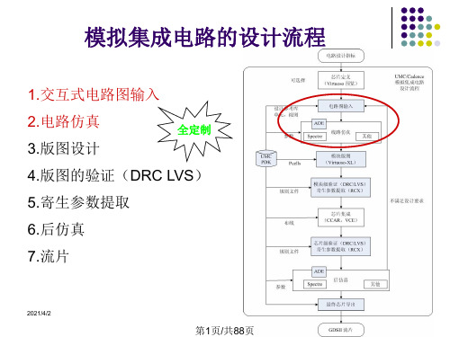
ADS软件的使⽤⼿册编写及应⽤_1_ADS软件的使⽤⼿册编写及应⽤⼀.关于ADS软件⼀)ADS中的projects当⽤户对ADS中的designs进⾏建⽴,模拟和分析以完成设计任务时,将会产⽣⼀定量的数据,⽽projects正是对这些数据进⾏⾃动的组织和存储。
⼀个project包括:电路(circuit),版⾯(layout),模拟(simulation),分析(analysis)以及由于⽤户建⽴的designs和projects之间的连结⽽产⽣的designs的输出信息。
使⽤ADS的主窗⼝可以建⽴或打开projects。
当⽤户登陆ADS时,主窗⼝将被打开。
⼆)ADS中的designsADS中的designs是⽤来存储⽤户为完成设计任务⽽⽣成的原理图及版⾯设计信息。
⼀个designs包括:⼀个单独的原理图或电路图,或者包括若⼲原理图或电路图嵌⼊式的包含于⼀个单独的design中。
所有的designs都可以直接从主窗⼝打开或者从design窗⼝打开。
在⼀个design窗⼝中,⽤户可以做以下事情:建⽴或修改电路图和布线图增加变量和等式配置电路元件和模拟控制器制定版⾯,选择参数添加注释以及例证从电路中产⽣版⾯(版⾯中产⽣电路图)三)ADS中的模拟ADS软件提供模拟控制器功能,以便⽤户可以添加或配置模拟来测试⽤户的设计。
对于DSP设计来说,当⼀个模拟/射频设计仿真需要⼀个或多个不同的控制器时,就需要⼀个数据流控制器。
⽤户可以⾃⼰添加合适的控制器,也可以插⼊⼀个包含合适控制器的模板(template)。
模拟控制器的分类:1.数据流控制器:在使⽤Agilent Ptolemy模拟器时,⽤来控制混合同步数字信号来进⾏数字信号处理。
适⽤于所有的DSP设计。
2.DC :是射频/模拟电路设计模拟的基本控制器,提供拓扑检测和直流分析的功能。
适⽤于所有的射频/模拟设计。
3.AC:获得⼩信号转换参数,如电压增益,电流增益,线性电压或电流噪声。

仿真⼀般原则【转贴】感谢原创作者!电路仿真,⽆论在ADS还是spectreRF/spectre中,某种类型电路(譬如mixer、LNA、VCO等)原本该选择什么类型仿真(譬如Tran、PSS、HB、Env等)就先选择那种类型仿真,得到想要的结果(譬如噪声、频谱、增益、S参数等)。
但是,⼀种情况,遇到仿真时间过长(譬如⼏天,以致⽆法容忍)的时候,不妨尝试另⼀种仿真类型,譬如Tran仿真消耗时间太长,那么可以考虑Env,PSS仿真时间过长也以考虑Env。
当然,这种情况下,还应该考虑仅仿真所需数据,不需要观察输出的数据点应当在仿真之初就设置不要,譬如PSP和PAC的噪声仿真差异。
另外⼀种情况,当常规类型仿真⽆法收敛的时候,不妨尝试另⼀种仿真类型,譬如PSS在信号源是数字调制的电路中或者输⼊信号源是周期的但输出却杂乱⽆章的电路中,PSS或失效或效率低下,此时,选择Env可能奏效,最坏情况下再选择Tran(最多牺牲时间)也应该满⾜要求。
注意每种类型仿真都有其适应的条件(譬如PSS的周期性和近似线性、Env的频谱占有率⾼但是空隙⼤),满⾜这个条件,则仿真⾼效率运⾏;不满⾜,即便满负荷运⾏完毕,也得不到想要观察的数据。
仿真只是⼀个⼯具,在熟练应⽤⼯具的基础上,不沉溺于⼯具本⾝,但是也不强调⼯具⽆⽤论。
电路、系统理论掌握是基础、是根本,⼯具起到辅助作⽤。
适当的了解⼯具运⾏原理,知其所以然,会使其⽤起来更为得⼼应⼿,⽆论仿真中遇到什么问题都能果断推测源头所在,⽽不是盲⽬改电路或者改仿真设置。
我以为,⼯具应⽤的最⾼境界,就是看完⼀个电路,能估计出某种合适的仿真需要花费多久时间,最为致效。
这就需要知道电路中计算⽅程的数量、计算机本⾝硬件开销、仿真算法的重复次数以致满⾜收敛误差。
通常不需要了解这么多。
spectreRF Summary1. Noise FigureQPSS and QPnoise:当输⼊出现两个⼤的⼲扰信号的时候,⽤此分析来决定NF;PSS and Pnoise:当输⼊没有⼲扰信号存在的时候,⽤此分析来决定NF;PSS and PSP:即可奏效;SP:即可奏效;2. HarmonicsPSS:单纯的基于输⼊的点频来输出频谱成分(区别于输⼊扫描),即可以单⼀输⼊频率,⼜可以多个输⼊频率(在信号源中设置即可),都将产⽣指定数量的谐波成分,分析各次谐波、交调结果。
实验九、最终系统和电路仿真概述这是最后一个实验,把课程中的所有电路放在一起:放大器和滤波器。
它们代替了在前面实验中使用的特性(behavioral)系统模型。
任务●在系统中为1900MHz放大器构造一个子电路。
●使用Smart Simulation Wizard(灵活仿真魔术棒)。
●建立一个具有GSM源的谐波平衡仿真,并对它进行仿真。
●用CDMA源建立并运行一个CE仿真。
●运用一个数据显示例子,对ACPR和功率谱进行仿真。
●编程Marker sliders(游标)来规范(customize)数据显示。
●选作:具有最少指示的联合仿真。
目录1.为库创建最终Amp_1900子电路 (148)2.用灵活仿真魔术棒(Smart Simulation Wizard)对AMP_1900进行仿真 (149)3.创建一个由扫描LO的HB(谐波平衡)最终原理图和方程 (153)4.谐波平衡(HB)最终仿真:具有本振功率和噪音扫描的双音分析 (155)5.查看NF,Conv Gain,dbm_out和IF gain并作图 (157)6.最终的包络仿真:CDMA源 (157)7.打开一个DDS的例子,对ACPR和功率谱作图 (158)8.用一个编程的游标(marker slider)作频谱图 (160)9.选作:RF特性系统的联合仿真 (162)步骤1.为库创建最终AMP_1900子电路a.用一个新名AMP_1900保存最后的放大器电路包络设计(ckt_env_gsm),这个原理图将成为一个你的系统任务中要用到最终的放大器设计。
b.如图所示.删去所有的仿真控制元件、变量、源等。
设置Vdc=5V。
在File>Design Parameters中将元件实例名改为AMP_1900,符号名为SYM_Amplifier。
同时,确定放置端口连结器(port connector)1和2到输入输出端。
检查电路并保存和关闭AMP_1900设计。
.SNNOISERuns periodic AC noise analysis on nonautonomous circuits in a large-signal periodic steady state..SNNOISE output insrc frequency_sweep [N1, +/-1]+ [LISTFREQ=(freq1 [freq2 ... freqN ]|none|all]) [LISTCOUNT=num ]+ [LISTFLOOR=val ] [LISTSOURCES=on|off].HBAC / .SNACRuns periodic AC analysis on circuits operating in a large-signal periodic steady state..HBAC frequency_sweep .SNAC frequency_sweep.HBXF / .SNXFCalculates transfer function from the given source in the circuit to the designated output..HBXF out_var frequency_sweep .SNXF out_var frequency_sweep.PTDNOISECalculates the noise spectrum and total noise at a point in time..PTDNOISE output TIME=[val |meas |sweep ] +[TDELTA=time_delta ] frequency_sweep+[listfreq=(freq1 [freq2 ... freqN ]|none|all)] [listcount=num ]+[listfloor=val ] [listsources=on|off]RF OptionsSIM_ACCURACY=x Sets and modifies the size of the time steps. The higher the value, thegreater the accuracy; the lower the value, the faster the simulation runtime. Default is 1.TRANFORHB=n 1 Forces HB analysis to recognize or ignore specific V/I sources, 0 (default) ignores transient descriptions of V/I sources.HBCONTINUE=n Specifies whether to use the sweep solution from the previous simulation as the initial guess for the present simulation. 0 restarts each simulation in a sweep from the DC solution, 1 (default) uses the previous sweep solution as the initial guess.HBSOLVER=n Specifies a preconditioner for solving nonlinear circuits. 0 invokes the direct solver. 1 (default) invokes the- matrix-free Krylov solver. 2 invokes the two-level hybrid time-frequency domain solver.SNACCURACY=n Sets and modifies the size of the time steps. The higher the value, the greater the accuracy; the lower the value, the faster the simulation runtime. Default is 10.SAVESNINIT=”filename ” Saves the operating point at the end of SN initialization.LOADSNINIT=”filename ” Loads the operating point saved at end of SN initialization.Output Commands.BIASCHK .MEASURE .PRINT .PROBEFor details about all commands and options, see the HSPICE ® Reference Manual: Commands and Control Options.Synopsys Technical Publications 690 East Middlefield Road Mountain View, CA 94043Phone (650) 584-5000 or (800) Copyright ©2017 Synopsys, Inc. All rights reserved.Signal Integrity Commands.LINCalculates linear transfer and noise parameters for a general multi-port network..LIN [sparcalc [=1|0]] [modelname=modelname ] [filename=filename ]+ [format=selem|citi|touchstone|touchstone2] [noisecalc [=1|0]]+ [gdcalc [=1|0]] [dataformat=ri|ma|db]+ [listfreq=(freq1 [freq2 ... freqN ]|none|all)] [listcount=num ]+ [listfloor=val ] [listsources=1|0|yes|no].STATEYEPerforms Statistical Eye Diagram analysis..STATEYE T=time_interval Trf=rise_fall_time [Tr=rise_time ] + [Tf=fall_time ] Incident_port=idx1[, idx2, … idxN ]+ Probe_port=idx1[, idx2, … idxN ] [Tran_init=n_periods ] + [V_low=val ] [V_high=val ] [TD_In=val ] [TD_PROBE=val ]+ [T_resolution=n ] [V_resolution=n ] [VD_range=val ]+ [EDGE=1|2|4|8] [MAX_PATTERN=n ] [PATTERN_REPEAT=n ] + [SAVE_TR=ascii] [LOAD_TR=ascii] [SAVE_DIR=string ]+ [IGNORE_Bits=n ] [Tran_Bit_Seg=n ]+ [MODE=EDGE|CONV|TRAN] [XTALK_TYPE = SYNC|ASYNC|DDP|NO|ONLY]+ [Unfold_Length=n ] [TXJITTER_MODE = 1|2]RF Analysis Commands.ACPHASENOISEHelps interpret signal and noise quantities as phase variables for accumulated jitter for closed-loop PLL analysis..ACPHASENOISE output input [interval ] carrier=freq+ [listfreq=(freq1 [freq2 ... freqN ]|none|all)][listcount=num ]+ [listfloor=val ] [listsources=1|0].HBRuns periodic steady state analysis with the single and multitone Harmonic Balance algorithm..HB TONES=F1[,F2,…,FN ] [SUBHARMS=SH ] [NHARMS=H1[,H2,…,HN ]]+ [INTMODMAX=n ] [SWEEP parameter_sweep ].SNRuns periodic steady state analysis using the Shooting Newton algorithm..SN TRES=Tr PERIOD=T [TRINIT=Ti ] [MAXTRINITCYCLES=integer ]+ [SWEEP parameter_sweep ] [NUMPEROUT=val ].SN TONE=F1 [TRINIT=Ti ] NHARMS=N [MAXTRINITCYCLES=integer ]+ [NUMPEROUT=val ] [SWEEP parameter_sweep ].HBOSC / .SNOSCPerforms analysis on autonomous oscillator circuits..HBOSC TONE=F1 NHARMS=H1+ PROBENODE=N1,N2,VP [FSPTS=NUM,MIN,MA X]+ [SWEEP parameter_sweep ] [SUBHARMS=I ] [STABILITY=-2|-1|0|1|2].SNOSC TONE=F1 NHARMS=H1 [TRINIT=Ti ]+ [OSCTONE=N ] [MAXTRINITCYCLES=N ]+ [SWEEP parameter_sweep ].PHASENOISEInterprets signal / noise quantities as phase variables for accumulated jitter in closed-loop PLL analysis..PHASENOISE output frequency_sweep [method= 0|1|2]+ [listfreq=(freq1 [freq2 ... freqN ]|none|all)] [listcount=num ]+ [listfloor=val ] [listsources=1|0] [carrierindex=int ].HBNOISEPerforms cyclo-stationary noise analysis on circuits in a large-signal periodic steady state..HBNOISE output insrc parameter_sweep [N1, N2, ..., NK ,+/-1]+ [LISTFREQ=(freq1 [freq2 ... freqN ]|none|all]) [LISTCOUNT=num ]+ [LISTFLOOR=val ] [LISTSOURCES=on|off].NOISERuns noise analysis in frequency domain..NOISE v(out ) vin [interval ] [listckt[=1|0]]+ [listfreq=freq1 [freq2 ... freqN ]|none|all]) [listcount=num ]+ [listfloor=val ] [listsources=1|0|yes|no]] [listtype=1|0].ALTERReruns a simulation using different parameters and data from a specified sequence or block. The .ALTER block can contain element commands and .AC, .ALIAS, .DATA, .DC, .DEL LIB, .HDL, .IC (initial condition), .INCLUDE, .LIB, .MODEL, .NODESET, .OP, .OPTION, .PARAM, .TEMP, .TF, .TRAN, and .VARIATION commands..ALTER title_string.DCPerforms DC analyses..DC var1 START=start1 STOP=stop1 STEP=incr1Parameterized Sweep.DC var1 start1 stop1 incr1 [SWEEP var2 type np start2 stop2].DC var1 START=[par_expr1] STOP=[par_expr2] STEP=[par_expr3]Data-Driven Sweep.DC var1 type np start1 stop1 [SWEEP DATA=datanm (Nums )].DC DATA=datanm [SWEEP var2 start2 stop2 incr2].DC DATA=datanm (Nums )Monte Carlo Analysis.DC var1 start1 stop1 incr1 [SWEEP MONTE=MCcommand ].DC MONTE=MCcommand.OPCalculates the operating point of the circuit..OP format_time format_time ... [interpolation].PARAMDefines parameters. Parameters are names that have associated numeric values or functions..PARAM ParamName = RealNumber | ‘AlgebraicExpression’ | DistributionFunction (Arguments ) | str(‘string’) | OPT xxx (initial_guess, low_limit, upper_limit )Monte Carlo Analysis.PARAM mcVar = UNIF(nominal_val , rel_variation [, multiplier ]) | AUNIF(nominal_val , abs_variation [, multiplier ])| GAUSS(nominal_val , rel_variation , num_sigmas [, multiplier ]) | AGAUSS(nominal_val , abs_variation , num_sigmas [, multiplier ]) | LIMIT(nominal_val , abs_variation ).STOREStarts creation of checkpoint files describing a running process during transient analysis..STORE [file=checkpoint_file ] [time=time1]+ [repeat=checkpoint_interval ].TEMPPerforms temperature analysis at specified temperatures..TEMP t1 [t2 t3 ...].TRANPerforms a transient analysis.Single-Point Analysis.TRAN tstep1 tstop1 [START=val ] [UIC]Multipoint Analysis.TRAN tstep1 tstop1 [tstep2 tstop2 ... tstepN tstopN ]+ RUNLVL =(time1 runlvl1 time2 runlvl2...timeN runlvlN )+ [START=val ] [UIC] [SWEEP var type np pstart pstop ]Monte Carlo Analysis.TRAN tstep1 tstop1 [tstep2 tstop2 ... tstepN tstopN ]+ [START=val ] [UIC] [SWEEP MONTE=MCcommand ]Invoking HSPICESimulation Modehspice [-i] input_file [-o [output_file ]] [-hpp] [-mt #num ][-gz] [-d] [-case][-hdl filename ] [-hdlpath pathname ] [-vamodel name ]Distributed-Processing Modehspice [-i] input_file [-o [output_file ]] -dp [#num ][-dpconfig [dp_configuration_file ]] [-dplocation [NFS|TMP][-merge]Measurement Modehspice -meas measure_file -i wavefile -o [output_file ]Help Modehspice [-h] [-doc] [-help] [-v]Argument Descriptions-i input_file Specifies the input netlist file name.-o output_file Name of the output file. HSPICE appends the extension .lis.-hpp Invokes HSPICE Precision Parallel.-mt #num Invokes multithreading and specifies the number of processors. Works best when -hpp is used.-gz Generates compression output on analysis results for these output types: .tr#, .ac#, .sw#, .ma#, .mt#, .ms#, .mc#, and .print*.-d (UNIX) Displays the content of .st0 files on screen while running HSPICE.-case Enable case sensitivity.-hdl filename Specifies a Verilog-A file.-hdlpath pathname Specifies the search path for Verilog-A files.-vamodel name Specifies the cell name for Verilog-A definitions.-dp #num -dpconfig dpconfig_file -dplocation [NFS|TMP] Invokesdistributed processing and specifies number of processes, the configuration file for DP, and the location of the output files.-merge Merge the output files in the distributed-processing mode.-meas measure_file Calculates new measurements from a previous simulation.-h Outputs the command line help message.-doc Opens the PDF documentation set for HSPICE (requires Adobe Acrobat Reader or other PDF document reader).-help Invokes the online help system (requires a Web browser).-v Outputs HSPICE version information.HSPICE is fully integrated with the Synopsys® Custom Compiler™ Simulation and Analysis Environment (SAE). See the Custom Compiler™ Simulation and Analysis Environment User Guide .To use the HSPICE integration to the Cadence® Virtuoso® Analog Design Environment, go to /$INSTALLDIR/interface/ and follow the README instructions.Analysis Commands.ACPerforms AC analyses.Single / Double Sweep.AC type np fstart fstop.AC type np fstart fstop [SWEEP var+ [START=]start [STOP=]stop [STEP=]incr ].AC type np fstart fstop [SWEEP var type np start stop ]Sweep Using Parameters.AC type np fstart fstop [SWEEP DATA=datanm (Nums )].AC DATA=datanm.AC DATA=datanm [SWEEP var [START=]start [STOP=]stop [STEP=]incr ].AC DATA=datanm [SWEEP var type np start stop ]Monte Carlo Analysis.AC type np fstart fstop [SWEEP MONTE=MCcommand ].LSTBInvokes loop stability analysis..LSTB [lstbname ] mode=[single|diff|comm + vsource=[vlstb |vlstbp,vlstbn ]Data-Driven Sweep.TRAN DATA=datanm.TRAN DATA=datanm [SWEEP var type np pstart pstop ].TRAN tstep1 tstop1 [tstep2 tstop2 ... tstepN tstopN ]+ [START=val ] [UIC] [SWEEP DATA=datanm (Nums )]Time Window-based Speed/Accuracy Tuning by RUNLVL.TRAN tstep tstop [RUNLVL=(time1 runlvl1...timeN runlvlN )]Circuit Block-based Speed/Accuracy Tuning by RUNLVL.TRAN tstep tstop+ [INST=inst_exp1 RUNLVL=(time11 runlvl11...time1N runlvl1N )]+ [SUBCKT=subckt_exp2 RUNLVL=(time21 runlvl21...time2N runlvl2N )]Time Window-based Temperature Setting.TRAN tstep tstop [tempvec=(t1 Temp1 t2 Temp2 t3 Temp3...)+[tempstep=val ]].TRANNOISEActivates transient noise analysis to compute the additional noise variables over a standard .TRAN analysis..TRANNOISE output [METHOD=MC] [SEED=val ] [SAMPLES=val ] [START=x ]+ [AUTOCORRELATION=0|1|off|on] [FMIN=val ] [FMAX=val ] [SCALE=val ]+ [PHASENOISE=0|1|2] [JITTER=0|1|2] [REF=srcName ] [PSD=0|1]HSPICE Options.OPTION opt1 [opt2 opt3 …]opt1 opt2 … Specify input control options.General OptionsALTCC=n Enables reading the input netlist once for multiple .ALTER statements. Default is 0.LIS_NEW=x Enables streamlining improvements to the *.lis file. Default is 0. SCALE=x Sets the element scaling factor. Default is 1.POSTTOP=n Outputs instances up to n levels deep. Default is 0.POSTLVL=n Limits data written to the waveform file to the level of nodes specified by n .POST=n Saves results for viewing by an interactive waveform viewer. Default is 0.PROBE=n Limits post-analysis output to only variables specified in .PROBE and .PRINTstatements. Default is 0.RC Reduction OptionsSIM_LA=name Starts linear matrix (RC) reduction to the PACT, PI, or LNE algorithm. Defaultis off.Transient OptionsAUTOSTOP=n Stops transient analysis after calculating all TRIG-TARG, FIND-WHEN, andFROM-TO measure functions. Default is 0.METHOD=name Sets numerical integration method for a transient analysis to GEAR, or TRAP(default), or BDF.RUNLVL=n Controls the speed and accuracy trade-off; where n can be 1 through 6. The higher the value, the greater the accuracy; the lower the value, the faster the simulation runtime. Default is 3.Variability and Monte Carlo Analysis.AC .DC .TRAN .MEASURE .MODEL .PARAM .ACMATCHCalculates the effects of variations on the AC transfer function, with one or more outputs..ACMatch Vm(n1) Vp(n1) Vr(n1) Vi(n1) Vm(n1,n2) Im(Vmeas ).DCMATCHCalculates the effects of variations on the DC operating point, with one or more outputs..DCMatch V(n1) V(n1,n2) I(Vmeas )。
Agilent EEsof EDAAdvanced Design SystemFor Designs that Live Up to Your Dreams“We were pleasantly surprised to learn that Agilent EEsof EDA offers affordable choic-es for growing compa-nies like us. They set the standard for high-frequency design soft-ware and have the broadest range of simu-lation capabilities. I'm confident that we have chosen a toolset that can expand with us as we grow.” Steven J. Bennett Vice President of Research andDevelopment, UnityWireless SystemsIn Gary Smith EDA’s 2009 market share report, Agilent EEsof wasrecognized as the leading provider of RF Design and Simulation tools.For designs that live up to your dreams,choose software that lives up to your designsAs technology and competition acceler-ate, so do the challenges of getting to market first, with better, smaller, and fast-er products. Today, it is critical for engi-neers to be productive and effective. Efficiently exploring different design pos-sibilities requires powerful tools and meth-odologies.Agilent understands these challenges first-hand. Our diverse electronic products and test and measurement businesses include designers of RF and microwave semiconductor products such as duplex-ers, filters, mixers, and RFICs. Our own fabrication facilities include Si and GaAs processes for manufacturing circuits and components such as mixers, attenuators, prescalers, switches, and power amplifier ICs – all used extensively in today’s sophisticated communications products. Our EDA business grew out of an internal need to improve the design process for RF and microwave test instrumentation. The business quickly grew to division sta-tus, with a long history of innovation that continues today, including many patented technologies and current patents pending. With the introduction of the Touchstone linear simulator more than 20 years ago, Agilent EEsof EDA has led the develop-ment of new high-frequency EDA technol-ogies such as Harmonic Balance and Circuit Envelope simulators, RF/analog/baseband co-simulation and behavioralMost popular high-frequency design softwareAdvanced Design System (ADS) is the industry leader in high-frequency design. It supports system and RF design engineers developing all types of RF designs, from simple to the most complex, from RF/microwave modules to integrated MMICs for communications and aerospace/defense applications. With a complete set of simulation technologies ranging from frequencyand time-domain circuit simulation to electromagnetic field simulation, ADS lets designers fully characterize and optimizedesigns. The single, integrated design environment provides system and circuit simulators, along with schematic capture, layout, and verification capability – elimi-nating the stops and starts associated with changing design tools mid-cycle. Agilent EEsof EDA offers a wide variety of flexible plans to work within your budget. Time-based licenses and limited-term packages are available to get you the tools you need today. As your design needs grow, you can add simulators,models, and libraries as you require them.models. It is technology that has proven its robustness and lasting value over time.More focus on design – less on learningTime-to-market pressures often don’t accommodate learning a new software package. To help designers get to first-cut design results, ADS supplies over 300 examples or start from templates. ADS supplies over 300 examples, accessed through a powerful search engine. Each example gives instructions for using ADS, enabling you to focus on the design, and not on the design tool.Data display for the big pictureIf your simulation results do not allow you to see at a glance how your design is performing, you’re losing productivity. The strong data analysis and display technology in ADS lets you view results in the many ways you may want tosee them. Post processing capabilitiesDesignGuides for expert helpAgilent EEsof EDA has more than a dozen industry experts using theirexperience and best practices to create application-oriented ADS DesignGuides. DesignGuides make the job of circuit design easier, faster, and more consistent with wizards, pre-configured set-ups and displays, and step-by-step instructions. Complete design applications such as amplifiers, filters, mixers, microstripcircuits, RF systems, Bluetooth, and ultra-wideband designs, to name just a few, give you easy access to the power of ADSwithout taking time to learn from scratch.“I collaborate with Agilent EEsof EDA because they have the largest customer base to potentially benefit from my expertise. The open architecture of the ADS platform makes it easy for application specialists like me to develop DesignGuides. The time I put into a DesignGuide is time saved in engineering cycles.”Dr. Michael Jensen Professor of Electrical Engineering, Brigham Young University and Vice President of AJ Design GroupDesignGuides and templates in ADS make displaying simulation results easy.The ADS optimization cockpit provides an interactive environment with multiple optimization variables, interactive tuning and progress controls. Achieve the best performance while gaining design insight of the optimized variables versus the goals.let you manipulate data using custom expressions, view data on different plots, and change specifications, all without re-simulating.Design Libraries for easier wireless designFor cutting-edge wireless design, ADS Design Libraries help get emerging wire-less products to market faster. By building the latest signal formats into ADS, you can spend your time on new design ideas, not on researching the standards. Design Libraries contain pre-configured schemat-ics, data displays, and test benches to help you verify designs against measure-ments defined in the wireless standards specifications.The widest choice in models– from Process Design Kits to custom extractionDesign kits for foundry process compatibilityAgilent works with top foundries around the world to develop and support process design kits for RFIC and MMIC design in ADS. Kits are maintained by the foundry,so you can be sure they provide the most accurate and up-to-date models for their latest process, as well as the most com-prehensive design automation features.High-quality models for accuracyAccurate models are a prerequisite for any successful design flow. Without good models, designers can’t make progress or have confidence in their simulation results.ADS has models for every microwave and RF design application:• RF System models provide gain blocks, mixers, filters, modulators and demodu-lators, PLL components, and passive elements for accurate and easy system design.• All the major component vendorsprovide up-to-date component libraries specifically for ADS.• Component libraries have over 100,000 parts. Many contain auto-layout capa-bilities for creating a layout directly from schematic for design rule check-ing or planar EM simulation.• Design Libraries contain models for the latest communication standard modu-lation formats, including 3GPP LTE, HSPA, Mobile/Fixed WiMAX™, DTMB, CMMB, WVAN, CDMA, GSM, DTV, 802.11n, TD-SCDMA, WLAN, W-CDMA, CDMA2000/1xEV, EDGE, WiMedia.Several options allow you to develop cus-tomized models that meet your specific device and product requirements:• Advanced Model Composer, based on a patented technology, uses EM simulation to create accurate passive models that have the simulation speed advantages of analytical models.• Verification Model Extractor creates system-level behavioral models from device-level circuit designs for faster system-level verification.• Analog Model Development Kit gener-ates user-defined circuit and system models for integrating proprietary behavioral models.• Verilog-A compiler allows the simula-tion of custom device models and behavioral models in Verilog-A format.Agilent also provides modeling systems to develop accurate device model extrac-tions.“ADS is an important toolset to support. It has the widest usage among our customer base and within TriQuint.”Eli Reese Director ofDesign Engineering at TriQuint Semiconductorin Richardson, Texas.AC/S-Parameters High Speed Interconnect LibraryHarmonic BalanceCo-Simulation with 3rd Party Simulators Agilent Ptolemy Timed Synchronous DataflowCircuit EnvelopeTransient ConvolutionMomentumP h y s i c a lN u m e r i cT i m eF r e q u e n c yAdvanced Model ComposerFinite ElementADS Simulation TechnologyAdvancing TechnologyD o m a i nIndustry-leading simulation technology – circuit to system, simple to complexSimulator technology handles size, complexity, with easeDesigning circuits for different functional blocks often requires an array of simula-tion technologies. ADS offers the most complete set of simulation technologies available today in a single software pack-age. Combined, they enable you to fully characterize and optimize designs under varied conditions without simulator-imposed limitations on accuracy, depth, or detail. The result is a design that can exceed performance requirements and be manufactured at high volumes.Simulator highlights:• For system-level simulation, Agilent Ptolemy is the only commercially available timed synchronous data flow co-simulate with the analog and RF simulators, allowing you to see the effects that circuit-level blocks have on system-level results, for a true mixed-signal analysis.• When it was introduced in the early 1980s, Harmonic Balance was the first commercially available simulator of its kind. Over time, it has developed into the most advanced frequency-domain simulator for fast analysis of nonlinear circuits. Today, it can handle large-scale ICs with thousands of transistors. It also simulates digital frequency-divider circuits using the Transient Assisted Harmonic Balance capability.• C ircuit Envelope is a patented ADS innovation that enables accurate analy-sis of time-varying carriers directly in the frequency domain. Only Circuit Envelope simulates time-varying signal response at the system level, allowingdirect and easy optimization of circuit performance. Key applications include modulator/ demodulator response, synthesizer hopping analysis, phase-lock-loop-based automatic frequency control response, oscillator stability and warm up, and automatic gain control/phase-lock-loop response to complex signals.• The RF System simulator contains a unique RF system budget analysis feature that lets you examine more than 40 system measurements such as third-order intercept, 1dBc, and noise figure for each component in the high-level system.The time-based Transient/Convolution simulator accounts for frequency- domain effects such as coupled transmission lines.ADS Layout information is combined with the Momentum substrate definition to produce a 3D spatial representation of circuit geometries.Co-simulation with LayoutComponents allows you toincorporate layout artwork inthe schematic environmentto enable concurrent analy-sis of circuit performancealong with critical physicaleffects.The Physical Connectivity Engine check connectivity fea-ture allows you to highlight any trace or interconnect. Itthen highlights all overlapping metal.From the spark of an idea to a verified design –Agilent EEsof EDA is committed to providing the most complete design flow. Where gaps exist that give designers pain and take up their time, we round out our product line and solutions to bridge them. Physical design predicts performanceAccurate implementation of physical design is important for predicting hard-ware performance. ADS includes a com-prehensive physical design environment specifically geared for high-frequency layout design and verification. It hostsa number of capabilities such as design synchronization with schematic, a physi-cal connecivity engine, integrated EM simulators, and a design rule checker (DRC). Layout allows designers to fully characterize artwork and improves the ability to catch errors prior to production. Physical Connectivity EngineWhen it comes to high-frequency design,traditional LVS tools often limit intercon-nect options to simple traces. Agilent’sPhysical Connectivity Engine lets you useany custom shape to build interconnects.The engine runs in the background andextracts interconnect information fromtraces, paths, vias, and custom polygons,in real time, allowing you to perform anumber of interconnect checks withoutlaunching a separate utility. The PhysicalConnectivity Engine also allows you toverify real-time-connectivity graphically onyour layout, providing a true representa-tion of interconnects. Better interconnectrepresentations reduce design uncertaintybefore prototyping, so you can be confi-dent that what you design in schematic iswhat you represent in layout.Momentum & FEM Simulatorfor EM AnalysisBoth Agilent’s Momentum and FiniteElement Method (FEM) simulators arefully integrated with the ADS layoutenvironment. Momentum is the leading3D planar electromagnetic (EM) simulatorused for multi-layer IC and PC Boardanalysis. The FEM simulator is based onfull 3D EM technology that can handle3D arbitrary shaped structures suchas connectors, conical shape vias andsolder balls/bumps where z-dimensionalchanges appear in the structure. Bothsimulators generate accurate EM modelsthat can be used directly with ADS circuitsimulators.Agilent’s X-parameters* represent a new category of nonlinear network parameters for high-frequency design. They are applicable to both large-signal and small-signal condi-tions, and for linear and nonlinear components.– with no break in the flowConnected SolutionsDesign verification using today’s complex communications signal formats is a chal-lenge. Designs can be analyzed early in simulation, and they can be verified later, after all of the hardware returns from fabrication – but designers don’t have the luxury of waiting for all of the hardware. They need an intermediate level of verification to cut overall design time and reduce risk.Agilent’s connected solutions allow verification very early in the prototyping cycle for applications ranging fromemerging wireless communications prod-ucts to aerospace/defense by integrating ADS with Agilent test instruments such as signal generators and signal analyzers to enable new design and verification capabilities. This unique combination allows the sharing of signals, measure-ments, algorithms, and data seamlessly between the virtual software and physical hardware domains. Designers use this linkage to simulate and evaluate design trade-offs and what-ifs and then turn the simulated signal into an RF test signal on the bench f or hardware test. Conversely, designers can take themeasured output signal from the DUT and bring it into ADS for additional analysis in the simulation environment.Design flow integration – partners for complete successAt Agilent EEsof EDA we align with key EDA vendors and frameworks to provide enhanced solutions that complement your investment. The open and flexible ADS environment ensures that a wide range of design flows is supported. For example, if your design flow is based on a Cadence, Mentor or Zuken flow, Agilent EEsof EDA supports these frameworks with integra-tion products using industry-standard formats. Our expanding list of partners goes well beyond standard relationships and is part of an ongoing effort to provide best-in-class tools and technology that work the way you work best—in anintegrated environment.New X-Parameter GeneratorX-parameter models are fast, cascadable,nonlinear behavioral models thataccurately account for frequency mixing and impedance mismatch. X-parameters fulfill a long standing need from the high-frequency design community for nonlinear behavioral models that can be created from measurement or simulation with the same speed and convenience as the well known linear S-parameters. The X-Parameter Generator enables MMIC,RF-SIP and RF module design houses to provide their customers with an accurate,pre-prototype model of their nonlinear devices (e.g. power amplifiers, front-end modules and transceivers) to further enable concurrent design and secureearly design wins.“Agilent’s design software and test hardware accelerates our design verification,giving us the confidence to begin prototyping”Eric HansenPresident and CEO of Innovative Wireless TechnologiesApplication Areas– from RF to microwave, from circuit to system,Microwave/MMIC design Reduce costs and get to market fast, and first. This is the challenge that MMIC designers face. ADS rises to this chal-lenge, making MMIC design faster and easier than ever before. ADS supports a complete, front-to-back flow by incorpo-rating Layout and all of the ADS simula-tion technologies (system, circuit, and electromagnetic) in a single, integrated design flow. All of today’s leading GaAs foundries actively maintain component design kits that support the powerful ADS simulation technologies.In microwave circuit design, the circuit and physical designs must be closely linked. ADS allows you to start a MMIC design in either the layout or schematic environment. The design synchronization engine controls and tracks design updates and supports multiple design synchronization modes to match your methodology.The ADS Layout components feature adds a new dimensionto MMIC design.You can bring alayout directly intothe schematicenvironment to giveyou access to EMsimulators withinyour circuit design.Or, you can bringin a DUT board –characterized bynetwork analyzermeasurements orby EM simulation– for concurrentmodeling of thedesign whileaccounting forboard or packagingeffects. Signal integrity/high-speed digital designSignal integrity is a major concern forengineers of high-data-rate designs, suchas Infiniband, PCI Express, and RapidIO.Meeting the demand for increasinglyfast circuits with high clock speeds is aconstant challenge. High-frequency ana-log effects such as reflection, cross talk,ground bounce, and propagation delaysthrough interconnects adversely affectsignal quality and timing performance.ADS has the right simulation tools andlibraries, including a multi-layer intercon-nect library that enables you to accuratelymodel and analyze high-speed intercon-nect problems before fabrication, resultingin lower development costs and fastertime to market.RFIC designAs today’s wireless and wireline applica-tions increase in frequency and speed,RFIC design engineers need access toaccurate and efficient high-frequencysimulation tools. Shorter product life-cycles and global competition continue toadd pressure for quality product designs.Agilent EEsof EDA has the most compre-hensive set of simulation tools, models,and verification features to increase therobustness of your RFIC designs.If your designs are based on the Cadenceflow, you can access Agilent’s powerfulfrequency-domain simulation technolo-gies directly from within the Cadenceenvironment using Agilent’s GoldenGate.Circuit netlists from the Cadence environ-ment can also be brought into ADS foranalysis using Dynamic Link. Either way,you’ve got the power to efficiently designRFICs with high performance and yield forcapitalizing on market opportunities.The Complete MMIC ADS Desktop Design Flow enable front-to-back design and simulation to physical design, verification and manufacturing.from board to package to RFIC – ADS is the tool of choiceCommunications system designToday, the complexities of system design are greater than ever. Designers working with recent and emerging wireless stan-dards such as 3GPP LTE, HSPA, Mobile/ Fixed WiMAX™, DTMB, CMMB, WVAN, CDMA, GSM, DTV, 802.11n, TD-SCDMA, WLAN, W-CDMA, CDMA2000/1xEV, EDGE, WiMedia, need to reduce design turns and get to market quickly with a complete system that satisfies the needs of RF/analog and baseband applications. Aerospace/defense industry designers also need quick design turns and rapid design verification when specifications are incomplete and measurements are highly specialized.Wireless communications product system designs must be partitioned into their baseband and RF portions. For the RF portion, ADS provides more behavioral models than any other EDA vendor – more than 1800 models in all. ADS design and model libraries are preconfigured for simulation and contain the most complete set of measurements available. When additional measurements are required, Connected Solutions fills the gap with signal generation, sharing, and analysis via instrument-software links.In aerospace/defense, Agilent’s con-nected solutions are particularly useful for extending the standard measurements provided by Agilent’s test instruments by combining them with ADS and its exten-sive library of behavioral models. RF Board designToday’s high-frequency RF board designerwants few board re-spins and high-yield designs. The integrated system,circuit, and EM simulators, Layout, andpowerful optimizers in ADS help increaseproductivity and efficiency, validating yourhigh-yield designs prior to manufacturing.Our focus on design flow integrationmeans that ADS works with your otherframework integration products, such asMentor, Cadence and Zuken.Integration also means that the ADSLayout tool is linked to the schematicenvironment. This back-annotating link,coupled with our integrated EM simulator,allows you to account for physical effectsthat could significantly affect designperformance. The Physical ConnectivityEngine detects wiring information that isso important to a correct layout, and feedsit to the interconnect checking featuresin ADS for an accurate representation oflayout interconnects.A growing list of up-to-date componentlibraries is available for ADS RF boarddesign. Agilent, component vendors, andmodeling companies regularly updatethese libraries, and we provide downloadaccess to them via the Agilent EEsof EDAweb site.An ever growing list of component vendorsprovide libraries for ADS. (Several of theseare offered by Modelithics, Inc.)• On Semiconductors• Panasonic• Philips• Polyfet• Presidio Components Inc.• Samsung• Samtec• SAMYOUNG• Skyworks• Taiyo Yuden• Temwell• TDK• Thin Film Technology (TFT)• Toko• Toshiba• Transcom• VishayGetting the most from ADSWorld-class supportyou need to ensure that support will be there when and where you need it. Agilent EEsof EDA has dedicated support engineers in many countries to provide you with local language support, including English, Japanese, Korean, Mandarin, French, German, and Dutch. Phone sup-port is available Monday through Friday, worldwide.of the way. They include software and user manual updates via download or on CD-ROM, worldwide technical support via telephone, fax, e-mail, and the worldwide web.In a world where not only your product goes international, but often your design team is also distributed across continents,Knowledge CenterIn the Knowledge Center, Maintenance Service Releases – with updates to previ-ously released software versions – are available for download. A tracking feature allows you to submit and manage your support cases and related defect and enhancement requests. A robust search function lets you quickly find available solutions and sort through them by date,popularity, or user ratings. The Knowledge Center also contains product discussion forums where you can converse with other users, support engineers, and product developers, along with recorded Technical Info Sessions and introductory e-Learning Short Courses.The Agilent EEsof EDA support web site, featuring the Agilent EEsof Knowledge Center, is an around-the-clock resource for designers. The Knowledge Centercontains thousands of support documents and hundreds of downloadable examples created by support engineers to supple-ment the ADS application examples and documentation.Agilent Technologies is committed to customer satisfaction. We are dedicated to providing the right software, support, and consulting solutions to increase your engineering productivity and advance your long-term success. Whether you are a novice or experienced user, Agilent EEsof EDA’s customer support offerings are designed to help you every step11Achieve business results faster with help from the expertsEvery design team’s flow has aspects that are unique. To save time and get indi-vidual attention focused on your particular design needs, take advantage of Agilent EEsof EDA’s consulting services. We offer complete consulting in MMIC, RFIC, RF board/module, or system-level design.• Device Modeling – We can quickly characterize and extract industry-stan-dard models for your device, and then (optionally) provide test structure and device layout design services.• P rocess Design Kits – Let us create or extend your custom PDK elements or libraries.• C onnected Solutions – Get start-up training in simulation plus instrumenta-tion set-up for X-parameters, 3G, LTE.• Simulation Assistance – Eliminate trial and error. Get expert coaching and learn best practices for complex circuits or systems.• Design Process Consulting – Let us perform an analysis of your design flow and make recommendations that will save you time and money.– with support, training, servicesTrainingHaving a good working knowledge of your EDA software can save precious time in the design cycle. Increased productivity and added expertise can contribute directly to your job satisfaction and to your company’s bottom line.Agilent EEsof EDA training offers a full range of classroom courses, as well as live and self-paced e-learning courses that teach the use of EDA software in a wide variety of applications. Live classes are conducted by experienced design engineers and focus on in-depth software operation and design examples, as well as covering introductory and advanced microwave, RF, System, and signal integrity design techniques. Self-paced e-learning courses allow you to set your own timetable. If you can’t travel to a regularly scheduled class and have agroup of designers who can benefit from a common class, your field sales represen-tative can arrange an on-site class.“I really appreciate the Agilent EEsof EDA training class.The presentation of ADS capabilities,such as how to simulate an entire communication link and integrate RF with Ptolemy, is excellent.”Peter DenneyRF/Antenna Engineer,Harris CorporationFor more information on AgilentTechnologies’ products, applications or services, please contact your local Agilent office. The complete list is available at:/find/contactus Americas Canada (877) 894 4414 Brazil (11) 4197 3500Mexico 01800 5064 800 United States (800) 829 4444Asia Pacific Australia 1 800 629 485China 800 810 0189Hong Kong 800 938 693India 1 800 112 929Japan 0120 (421) 345Korea 080 769 0800Malaysia 1 800 888 848Singapore 1 800 375 8100Taiwan 0800 047 866Other AP Countries (65) 375 8100 Europe & Middle East Belgium 32 (0) 2 404 93 40 Denmark 45 70 13 15 15Finland 358 (0) 10 855 2100France 0825 010 700**0.125 €/minuteGermany 49 (0) 7031 464 6333 Ireland 1890 924 204Israel 972-3-9288-504/544Italy39 02 92 60 8484Netherlands 31 (0) 20 547 2111Spain 34 (91) 631 3300Sweden0200-88 22 55United Kingdom 44 (0) 118 9276201For other unlisted Countries:/find/contactusRevised: October 14, 2010Product specifications and descriptions in this document subject to change without notice.© Agilent Technologies, Inc. 2001-2010Printed in USA, November 9, 20105988-3326EN/find/adsGet what you need today, with an eye to what you’ll need tomorrowExtensible design suites let you begin with a front-to-back solution that fits your budget, adding capabilities as you need them. ADS products range from eco-nomical foundation toolsets to advanced,comprehensive suites. Time-basedlicenses and limited-term packages also are available to give you the tools youneed just when you need them.ADS BundleIntegral to ADS CorePre-configured Element capabilities Provide powerful cost-effective functionalityADS Bundles come in different sizes and configurations to suit your design needsADS EnvironmentSimulators Design GuidesInstrument ConnectivityLayout ElementHarmonic Balance Element Momentum G2 ElementADS Product StructureThe flexible product structure of ADS lets you begin with pre-configured bundles and add capabilities as you need them.。