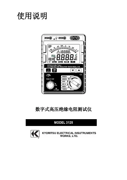
共立5410中文使用说明书
- 格式:pdf
- 大小:580.11 KB
- 文档页数:14
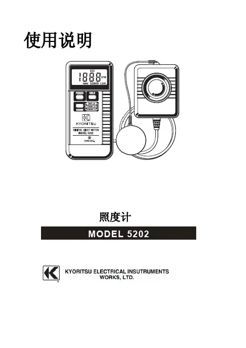
使用说明照度计MODEL 52021、特征●数据保留功能●受光传感器和仪器显示本体分离。
●偏斜调整功能。
●高照度测试。
●大型LCD显示,便于清晰读取数据。
2、规格●受光传感器:硅光电二极管●显示:最大值1999 的3 1/2 数字LCD显示屏,低电量显示,过量程显示:“OL”●测试量程刻度:0.1~19990Lux●测试量程选择:200/2000/20000Lux℃℃23±5●电池消耗:约2mA●响应速度:2.5次/秒●斜入受光特性:30°±3% 60°±10% 90°±30%●操作温湿度:0~50/℃℃低于80%R.H(无结露)●保存温湿度:-10~60/℃℃低于70%R.H(无结露)●电源:电池9V NEDA1604,IEC6F22,JIS 006P●尺寸:仪器本体 148mm×71mm×36 mm;受光部 85mm×67mm×32 mm●重量:仪器和受光部 约270g(包括电池)●附件:仪器本体;受光部;9V电池(安装);说明书;皮质盒3、面板各部分名称:1、LCD显示屏2、电源ON/OFF开关3、数据保留开关4、量程开关5、偏斜调整开关6、受光传感器7、受光传感器盖4、测试方法4.1 电源ON按下“POWER”开关打开照度计。
4.2 选择适当量程按“RANGE”开关选择200,2000,20000Lux。
4.3 偏斜调整若显示屏不能显示零,为了取得精确数据,请使用螺丝刀调整“ZERO ADJ.”使LCD显示000。
4.4 受光操作取下受光传感器的盖子。
将受光传感器放置于被测光源的测试点。
仪器将自动进行测试。
显示读数稳定后读取测试值。
(注意:为了提高读数的精确度,请尽量将受光传感器放置于垂直面向测试光源的位置。
4.5 数据保持操作使用者可保留当前读数并可按“HOLD”键使数据固定在LCD显示屏上。
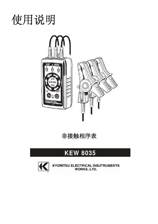
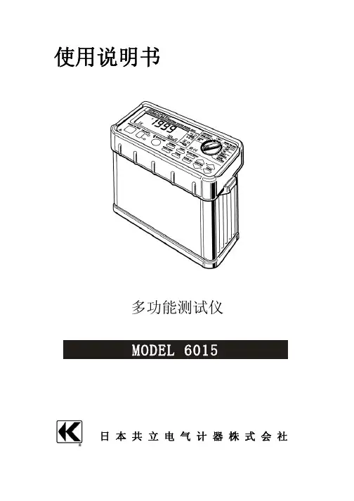
使用说明书多功能测试仪MODEL 6015目录1. 安全测试2. 介绍3. 仪表布局3.1 前面板3.2 测试端3.3 后面板3.4 测试线3.5 液晶显示屏4. 性能规格4.1 一般特性4.1.1 接地电阻4.1.2 绝缘电阻4.1.3 导通4.1.4 电源电压4.1.5 RCD4.1.6 回路阻抗4.1.7 PSC4.1.8 接地故障4.1.9 相序4.1.10 一般规格5. 测试5.1 一般说明5.1.1 旋转功能开关5.1.2 测试按钮5.1.3 膜式开关按钮5.1.4 接地电压触垫5.2 测试前安全检查步骤6. 导通测试6.1 仪表布局6.2 测试步骤7. 绝缘测试7.1 绝缘电阻的本质7.1.1 电容性电流7.1.2 传导电流7.1.3 表面泄漏电流7.1.4 总泄漏电流7.1.5 对压敏设备的损坏7.2 测量准备7.3 绝缘测试8.电源电压测量9. 回路阻抗测试9.1 电压测量9.1.1 故障回路电阻9.1.2 自动过热切断9.1.3 回路电阻测试9.2 回路阻抗测量9.3 三相设备回路阻抗10. 预期短路电流(PSC)测试10.1 预期短路电流10.2 测量预期短路电流11. 故障电流测试12. RCD测试12.1 RCD测试目的12.2 RCD测试方式12.3 RCD测试12.4 RCD测试辅助保护12.5 缓发型RCD测试时间12.6 测试直流灵敏RCD12.7 自动测量步骤13. 接地电阻测试13.1 标准的接地电阻测量13.2 检查重叠电阻区13.3 接地电阻测量14. 相序测量15. 存储功能—存储,清除,打印15.1 存储结果15.2 存储15.3 清除编号15.4 删除存储数据15.5 打印信息16. 更换电池17. 更换保险丝1 安全测试电是危险的,如果不够谨慎和缺乏安全性,将有可能造成伤害或死亡。
对待电,通常我们要保持高度的谨慎。
如果你不确定如何进行测量,请停止测量,并向专业人员咨询。

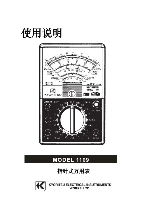
使用说明MODEL 1109指针式万用表目录1. 安全警告2. 特点3. 规格4. 各部件名称5. 测试准备工作6. 测试方法6-1 DC电压测试6-2 AC 电压测试6-3 低频输出 (dB) 测试6-4 AC 输出电压测试(使用输出端口)6-5 DC 电流测试6-6 15A AC 电流测试6-7 电阻测试6-8 端口间电流 LI, 端口间电压 LV 的测试6-9 晶体管h FE的测试7. 保险丝与电池的更换8. 其他1.安全警告●按国际安全规格IEC414标准进行设计和试验。
●为了避免触电等事故,正确使用仪器,使用前请阅读本说明书。
●本说明书使用危险和注意标志来表示使用中必须注意的事项,请仔细阅读。
危险是指避免引起触电等事故的注意事项,注意是指避免损坏仪器的注意事项。
●为确保安全请遵守以下注意事项。
(1) 测试前请确认选择了适当的测试量程。
特别是使用电流量程和电阻量程时请注意不要测试电压。
(2) AC15A端口和-COM端口插入测试线的状态时请不要测试电压。
(3) 电流测试中,测试棒离开回路时,测试棒与回路间可能产生高压。
请保证两者确实连接。
(4) 请将测试线的插头全车插入端口。
(5) 各量程上,请勿施加超过该量程的最大刻度值的电量。
(6) 测试物连接测试线的状态下,请勿更换量程。
(7) 测试仪的端口和接地间请勿施加超过AC/DC1000V的电压。
(8) 请勿在易燃场所测试(特别是电流测试)。
若产生火花容易导致爆炸。
(9) 使用中,测试仪本体和测试线若发现龟裂或金属部分暴露,请停止使用。
(10)更换电池,保险丝而打开后盖时,请先将测试线取下,量程开关设置为OFF。
(11)使用后请将量程开关设置为OFF。
(12)除了更换电池,保险丝之外请勿打开后盖。
(13)请使用指定保险丝。
(14)请勿测试250V以上工业用电力线。
(15)请勿长期放置于高温多湿,结露的场所和直射阳光下。
(16)请勿在超过50°温度的场所放置。
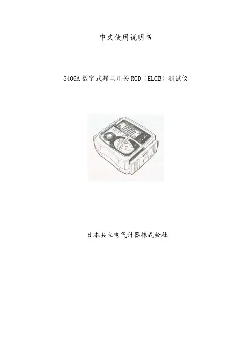
中文使用说明书5406A数字式漏电开关RCD(ELCB)测试仪日本共立电气计器株式会社目录1.警告2.操作说明3.特点4.技术规格5.测试6.测试7.维护8.携带1.警告1.1本仪器须由受过正规训练的、合格的技术人员进行操作,并在本手册规定的条件下使用。
由于用户使用不当、或违反本手册以及安全操作规定造成的设备损坏,共立公司(Kyoritsu )将不负责任何责任。
1.2使用前请仔细阅读并领会操作指南中所规定的内容。
使用本设备时请务必遵守相关的规定。
1.3本仪器可以放心使用。
然而,任何的安全措施均无法保障由于错误使用造成的对设备或人员的损害。
对于使用者而言,如果使用中麻痹大意或缺乏必要的操作训练,可能会因为自身原因造成在使用本设备时被电击或受到其它伤害。
1.4请仔细地、完整地阅读本手册。
1.5进行测量前请仔细检查量程开关以及所有的接线。
不要直接接触裸露的导线、接头或电路中任何标有“有电”(LIVE)的部分。
2.特性2.1 测试直流(DC)Sensitive断路器。
*2.2 本设备由微处理器控制,保证了最高的精度和可靠性。
2.3 触发时间数字显示。
2.4 常值电流源电路保证了主电压的波动将不会影响读数的精度。
测试电流与主电压相独立。
2.5 三个氖管用于检测连线状态。
2.6 结构紧凑、重量轻且易于使用。
2.7 弹性包装易于携带常用配件。
2.8 零点交错(Zero cross)电路保证了在0度和180度相位时进行测试。
在上述两点可以测出最小(最佳)和最大(最差)触发时间。
2.9 最大触发时间读数2000毫秒。
3.介绍3.1 5406A使用最新的微处理器技术,从而保证了产品的最佳性能及精度。
3.2 独立常值电流控制*常值电流电路保证了即使在230伏电压波动±10%的情况下仍能正确、稳定的读数。
3.3 DC Sensitive断路器*当5406A被设定为直流模式时,该仪器将测量30mA DC Sensitive断路器。
Single Channel, 16-Bit, Serial Input,Current Source DAC Preliminary Technical Data AD5410/AD5420Rev. PrEInformation furnished by Analog Devices is believed to be accurate and reliable. However, noresponsibility is assumed by Analog Devices for its use, nor for any infringements of patents or other rights of third parties that may result from its use. Specifications subject to change without notice. No license is granted by implication or otherwise under any patent or patent rights of Analog Devices. T rademarks and registered trademarks are the property of their respective owners. One Technology Way, P.O. Box 9106, Norwood, MA 02062-9106, U.S.A. Tel: 781.329.4700 Fax: 781.461.3113 ©2008 Analog Devices, Inc. All rights reserved.FEATURES12/16-Bit Resolution and MonotonicityCurrent Output Ranges: 4–20mA, 0–20mA or 0–24mA 0.1% typ Total Unadjusted Error (TUE)5ppm/°C Output DriftFlexible Serial Digital InterfaceOn-Chip Output Fault DetectionOn-Chip Reference (10 ppm/°C Max)Asynchronous CLEAR FunctionPower Supply (AV DD) Range10.8V to 60 V; AD5410/AD5420ACPZ10.8V to 40V; AD5410/AD5420AREZOutput Loop Compliance to AV DD – 2.5 V Temperature Range: -40°C to +85°CTSSOP and LFCSP PackagesAPPLICATIONSProcess ControlActuator ControlPLC GENERAL DESCRIPTIONThe AD5410/AD5420 is a low-cost, precision, fully integrated 12/16-bit converter offering a programmable current source output designed to meet the requirements of industrial process control applications.The output current range is programmable to 4mA to 20 mA, 0mA to 20mA or an over range function of 0mA to 24mA. The output is open circuit protected and can drive inductive loads of 1H. The device is specified to operate with a power supply range from 10.8 V to 40VAD5410/AD5420AREZ) or 10.8V to 60V(AD5410/AD5420ACPZ). Output loop compliance is 0 V to AV DD – 2.5 V.The flexible serial interface is SPI and MICROWIRE compatible and can be operated in 3-wire mode to minimize the digital isolation required in isolated applications.The device also includes a power-on-reset function ensuring that the device powers up in a known state and an asynchronous CLEAR pin which sets the output to the low end of the selected current range.The total output error is typically ±0.1% FSR.Table 1. Related DevicesPart Number DescriptionAD5422 Single Channel, 16-Bit, SerialInput Current Source andVoltage Output DACAD5412 Single Channel, 12-Bit, SerialInput Current Source andVoltage Output DACAD5410 Single Channel, 12-Bit, SerialInput Current Source DACAD5410/AD5420Preliminary Technical DataRev. PrE | Page 2 of 30TABLE OF CONTENTSFeatures..............................................................................................1 Applications.......................................................................................1 General Description.........................................................................1 Revision History...............................................................................2 Functional Block Diagram..............................................................3 Specifications.....................................................................................4 AC Performance Characteristics................................................6 Timing Characteristics................................................................7 Absolute Maximum Ratings............................................................9 ESD Caution..................................................................................9 Pin Configuration and Function Descriptions...........................10 Typical Performance Characteristics...........................................11 Terminology....................................................................................16 Theory of Operation......................................................................17 Architecture.................................................................................17 Serial Interface............................................................................17 power-up state.............................................................................21 Transfer Function.......................................................................21 Data Register...............................................................................21 Control Register..........................................................................21 RESET register............................................................................22 Status register..............................................................................22 Features............................................................................................23 fault alert......................................................................................23 Asynchronous Clear (CLEAR).................................................23 Internal Reference......................................................................23 External current setting resistor...............................................23 Digital Power Supply..................................................................23 External boost function.............................................................23 digital Slew rate control.............................................................24 I OUT Filtering Capacitors (LFCSP PAckage)............................25 Applications Information..............................................................26 driving inductive loads..............................................................26 Transient voltage protection.....................................................26 Layout Guidelines.......................................................................26 Galvanically Isolated Interface.................................................26 Microprocessor Interfacing.......................................................26 Thermal and supply considerations.........................................27 Outline Dimensions.......................................................................28 Ordering Guide.. (28)REVISION HISTORYPrE – Preliminary Version. May 2, 2008Preliminary Technical DataAD5410/AD5420Rev. PrE | Page 3 of 30FUNCTIONAL BLOCK DIAGRAMI OUT LATCH SCLK SDIN SDOCCAGNDCLEAR FAULT BOOSTREFOUT REFIN CLEAR SELECT R SETDV CC DGND**LFCSP PackageFigure 1.AD5410/AD5420Preliminary Technical DataRev. PrE | Page 4 of 30SPECIFICATIONSAV DD = 10.8V to 40V/60V 1, AGND = DGND = 0 V , REFIN= +5 V external; DV CC = 2.7 V to 5.5 V , R L = 300Ω, H L = 50mH; all specifications T MIN to T MAX , 0 to 24 mA range unless otherwise noted. Table 2.Parameter Value 2 Unit Test Conditions/Comments Output Current Ranges 0 to 24 mA 0 to 20 mA 4 to 20 mAACCURACYResolution 12 Bits AD5410 16 Bits AD5420 Total Unadjusted Error (TUE) ±0.3 % FSR max Over temperature, supplies, and time, typically 0.1% FSRTUE TC 3±5 ppm/°C typ Relative Accuracy (INL) ±0.024 % FSR max AD5410 ±0.012 % FSR max AD5420 Differential Nonlinearity (DNL) ±1 LSB max Guaranteed monotonic Offset Error ±0.05 % FSR max Offset Error Drift ±5 ppm FSR/°C typ Gain Error ±0.05 % FSR max @ 25°C, error at other temperatures obtained using gainTCGain TC 3±8 ppm FSR/°C max Full-Scale Error 0.05 % FSR max @ 25°C, error at other temperatures obtained using gainTCFull-Scale TC 3±8 ppm FSR/°COUTPUT CHARACTERISTICS 3Current Loop Compliance Voltage AVDD - 2.5 V max Output Current Drift vs. Time TBD ppm FSR/500 hr typ TBD ppm FSR/1000 hr typ Resistive Load 1200 Ω max Inductive Load 1 H max DC PSRR 1 µA/V max Output Impedance 50 MΩ typREFERENCE INPUT/OUTPUTReference Input 3Reference Input Voltage 5 V nom ±1% for specified performance DC Input Impedance 30 kΩ min Typically 40 kΩ Reference Range 4 to 5 V min to V max Reference Output Output Voltage 4.998 to 5.002 V min to V max @ 25°C Reference TC ±10 ppm/°C maxOutput Noise (0.1 Hz to 10 Hz)318 µV p-p typ Noise Spectral Density 3 120 nV/√Hz typ @ 10 kHzOutput Voltage Drift vs. Time 3±40 ppm/500 hr typ ±50 ppm/1000 hr typ Capacitive Load TBD nF max Load Current 5 mA typ Short Circuit Current 7 mA typLine Regulation 310 ppm/V typ Load Regulation 3 TBD ppm/mAThermal Hysteresis 3TBD ppmDIGITAL INPUTS 3DV CC = 2.7 V to 5.5 V, JEDEC compliant V IH , Input High Voltage 2 V min V IL , Input Low Voltage 0.8 V maxPreliminary Technical Data AD5410/AD54201 Maximum supply for the AD5410/AD5420BREZ is 40V, Maximum supply for the AD5410/AD5420BCPZ is 60V2 Temperature range: -40°C to +85°C; typical at +25°C.3 Guaranteed by design and characterization, not production tested.Rev. PrE | Page 5 of 30AD5410/AD5420 Preliminary Technical DataAC PERFORMANCE CHARACTERISTICSAV DD = 10.8V to 40V/60V1, AGND = DGND = 0 V, REFIN= +5 V external; DV CC = 2.7 V to 5.5 V, R L = 300Ω, H L = 50mH;all specifications T MIN to T MAX, 0 to 24 mA range unless otherwise noted.Table 3.Parameter2Unit Test Conditions/CommentsDYNAMIC PERFORMANCEOutput Current Settling Time TBD µs typ To 0.1% FSR , L = 1HTBD µs typ To 0.1% FSR , L < 1mHAC PSRR TBD dB 200mV 50/60 Hz sinewavesuperimposed on power supply voltage1 Maximum supply for the AD5410/AD5420BREZ is 40V, Maximum supply for the AD5410/AD5420BCPZ is 60V2 Guaranteed by design and characterization, not production tested.Rev. PrE | Page 6 of 30Preliminary Technical DataAD5410/AD5420Rev. PrE | Page 7 of 30TIMING CHARACTERISTICSAV DD = 10.8V to 40V/60V 1, AGND = DGND = 0 V , REFIN= +5 V external; DV CC = 2.7 V to 5.5 V , R L = 300Ω, H L = 50mH; all specifications T MIN to T MAX , 0 to 24 mA range unless otherwise noted. Table 4.Parameter 2, 3, 4 L imit at T MIN , T MAX Unit DescriptionWrite Modet 1 33 ns min SCLK cycle time t 2 13 ns min SCLK low time t 3 13 ns min SCLK high time t 4 13 ns min LATCH delay time t 5 40 ns min LATCH high time t 5 5 µs min LATCH high time (After a write to the CONTROL register) t 6 5 ns min Data setup time t 7 5 ns min Data hold time t 8 40 ns min LATCH low time t 9 20 ns min CLEAR pulsewidth t 10 5 µs max CLEAR activation timeReadback Modet 11 82 ns min SCLK cycle time t 12 33 ns min SCLK low time t 13 33 ns min SCLK high time t 14 13 ns min LATCH delay time t 15 40 ns min LATCH high time t 16 5 ns min Data setup time t 17 5 ns min Data hold time t 18 40 ns min LATCH low time t 19 40 ns max Serial output delay time (C L SDO 5 = 15pF) t 20 33 ns max LATCH rising edge to SDO tri-stateDaisychain Modet 21 82 ns min SCLK cycle time t 22 33 ns min SCLK low time t 23 33 ns min SCLK high time t 24 13 ns min LATCH delay time t 25 40 ns min LATCH high time t 26 5 ns min Data setup time t 27 5 ns min Data hold time t 28 40 ns min LATCH low time t 29 40 ns max Serial output delay time (C L SDO 5 = 15pF)1 Maximum supply for the AD5410/AD5420AREZ is 40V, Maximum supply for the AD5410/AD5420ACPZ is 60V 2Guaranteed by characterization. Not production tested. 3All input signals are specified with t R = t F = 5 ns (10% to 90% of DV CC ) and timed from a voltage level of 1.2 V. 4See Figure 2, Figure 3, and Figure 4. 5C L SDO = Capacitive load on SDO output.AD5410/AD5420Preliminary Technical DataRev. PrE | Page 8 of 30SCLKLATCHSDINCLEAROUTPUTFigure 2. Write Mode Timing DiagramSCLKLATCHSDINSDOSELECTED REGISTER DATA CLOCKED OUTFIRST 8 BITS ARE DON’T CARE BITSFigure 3. Readback Mode Timing DiagramSCLKSDINSDOLATCHFigure 4. Daisychain Mode Timing DiagramPreliminary Technical DataAD5410/AD5420Rev. PrE | Page 9 of 30ABSOLUTE MAXIMUM RATINGST A = 25°C unless otherwise noted.Transient currents of up to 100 mA do not cause SCR latch-up. Table 5.Parameter Rating AV DD to AGND, DGND −0.3V to 60V DV CC to AGND, DGND −0.3 V to +7 V Digital Inputs to AGND, DGND −0.3 V to DV CC + 0.3 V or 7 V(whichever is less)Digital Outputs to AGND, DGND −0.3 V to DV CC + 0.3 V or 7V(whichever is less)REFIN/REFOUT to AGND, DGND −0.3 V to +7 V I OUT to AGND, DGND −0.3V to AV DD AGND to DGND -0.3V to +0.3V Operating Temperature Range Industrial −40°C to +851°C Storage Temperature Range −65°C to +150°C Junction Temperature (T J max) 125°C 24-Lead TSSOP Package θJA Thermal Impedance 42°C/W 40-Lead LFCSP Package θJA Thermal Impedance 28°C/W Power Dissipation (T J max – T A )/ θJA Lead Temperature JEDEC Industry StandardSoldering J-STD-020Stresses above those listed under Absolute Maximum Ratings may cause permanent damage to the device. This is a stress rating only; functional operation of the device at these or any other conditions above those indicated in the operationalsection of this specification is not implied. Exposure to absolute maximum rating conditions for extended periods may affect device reliability.ESD CAUTION1Power dissipated on chip must be de-rated to keep junction temperature below 125°C. Assumption is max power dissipation condition is sourcing 24mA into Ground from AV DD with a 3mA on-chip current.Preliminary Technical DataAD5410/AD5420Rev. PrE | Page 10 of 30PIN CONFIGURATION AND FUNCTION DESCRIPTIONSSELECT R SETNCREFOUT DV CC NC I OUTAV DDD G N G N G N CG N DA V D D N CN CCV C CNC NC DV CC SELECT CCBOOST NCNC I OUT N R S E NC A G N CN N R E F I R E F O U CAP2CAP1Figure 5. TSSOP Pin ConfigurationFigure 6. LFCSP Pin ConfigurationPreliminary Technical DataAD5410/AD5420TYPICAL PERFORMANCE CHARACTERISTICSFigure 7. Integral Non Linearity vs. CodeFigure 8.Differential Non Linearity vs. CodeFigure 9. Total Unadjusted Error vs. CodeFigure 10. Integral Non Linearity vs. TemperatureFigure 11. Differential Non Linearity vs. TemperatureFigure 12. Integral Non Linearity vs. SupplyAD5410/AD5420Preliminary Technical DataFigure 13. Differential Non Linearity vs. Supply VoltageFigure 14. Integral Non Linearity vs. Reference VoltageFigure 15. Differential Non Linearity vs. Reference VoltageFigure 16. Total Unadjusted Error vs. Reference VoltageFigure 17. Total Unadjusted Error vs. Supply VoltageFigure 18. Offset Error vs. TemperaturePreliminary Technical DataAD5410/AD5420Figure 19. Gain Error vs. TemperatureFigure 20. Voltage Compliance vs. TemperatureFigure 21. I OUTvs. Time on Power-upFigure 22. I OUTvs. Time on Output EnabledFigure 23. DI CC vs.Logic Input VoltageFigure 24. AI DD vs AV DDAD5410/AD5420Preliminary Technical DataFigure 25. DV CC Output Voltage vs. DI CCLoad CurrentFigure 26. Refout Turn-on TransientFigure 27. Refout Output Noise (0.1Hz to 10Hz Bandwidth)Figure 28. Refout Output Noise (100kHz Bandwidth)Figure 29. Refout Line TransientFigure 30. Refout Load TransientPreliminary Technical Data AD5410/AD5420Figure 31. Refout Histogram of Thermal Hysteresis Figure 32. Refout Voltage vs. Load CurrentAD5410/AD5420 Preliminary Technical Data TERMINOLOGYRelative Accuracy or Integral Nonlinearity (INL)For the DAC, relative accuracy, or integral nonlinearity (INL), is a measure of the maximum deviation, in LSBs, from a straight line passing through the endpoints of the DAC transfer function. A typical INL vs. code plot can be seen in Figure 7 Differential Nonlinearity (DNL)Differential nonlinearity (DNL) is the difference between the measured change and the ideal 1 LSB change between any two adjacent codes. A specified differential nonlinearity of ±1 LSB maximum ensures monotonicity. This DAC is guaranteed monotonic by design. A typical DNL vs. code plot can be seen in Figure 8.MonotonicityA DAC is monotonic if the output either increases or remains constant for increasing digital input code. The AD5724R/AD5734R/AD5754R are monotonic over their full operating temperature range.Full-Scale ErrorFull-Scale error is a measure of the output error when full-scale code is loaded to the DAC register. Ideally, the output should be full-scale − 1 LSB. Full-scale error is expressed in percent offull-scale range (% FSR).Zero-Scale TCThis is a measure of the change in zero-scale error with a change in temperature. Zero-scale error TC is expressed in ppm FSR/°C. Gain ErrorThis is a measure of the span error of the DAC. It is the deviation in slope of the DAC transfer characteristic from ideal expressed in % FSR. A plot of gain error vs. temperature can be seen in Table TBDGain TCThis is a measure of the change in gain error with changes in temperature. Gain Error TC is expressed in ppm FSR/°C. Total Unadjusted ErrorTotal unadjusted error (TUE) is a measure of the output error taking all the various errors into account, namely INL error, offset error, gain error, and output drift over supplies, temperature, and time. TUE is expressed in % FSR.Current Loop Voltage ComplianceThe maximum voltage at the I OUT pin for which the output currnet will be equal to the programmed value.Power Supply Rejection Ratio (PSRR)PSRR indicates how the output of the DAC is affected by changes in the power supply voltage.Reference TCReference TC is a measure of the change in the reference output voltage with a change in temperature. It is expressed in ppm/°C. Line RegulationLine regulation is the change in reference output voltage due to a specified change in supply voltage. It is expressed in ppm/V. Load RegulationLoad regulation is the change in reference output voltage due to a specified change in load current. It is expressed in ppm/mA. Thermal HysteresisThermal hysteresis is the change of reference output voltage after the device is cycled through temperatures from +25°C to −40°C to +85°C and back to +25°C. This is a typical value from a sample of parts put through such a cycle. See Table TBDfor a histogram of thermal hysteresis.TCOOHYSOVVV__C)25(−°=6__10C)25(C)25()(×°−°=OTCOOHYSO VVVppmVwhere:V O(25°C) = V O at 25°CV O_TC = V O at 25°C after temperature cycleAD5410/AD5420 Preliminary Technical Data THEORY OF OPERATIONThe AD5410/AD5420 is a precision digital to current loopoutput converter designed to meet the requirements ofindustrial process control applications. It provides a highprecision, fully integrated, low cost single-chip solution forgenerating current loop outputs. The current ranges availableare; 0 to 20mA, 0 to 24mA and 4 to 20mA, The desired outputconfiguration is user selectable via the CONTROL register.ARCHITECTUREThe DAC core architecture of the AD5410/AD5420 consists oftwo matched DAC sections. A simplified circuit diagram isshown in Figure 33. The 4 MSBs of the 12/16-bit data word aredecoded to drive 15 switches, E1 to E15. Each of these switchesconnects 1 of 15 matched resistors to either ground or thereference buffer output. The remaining 8/12 bits of the data-word drive switches S0 to S11 of a 8/12-bit voltage mode R-2Rladder network.V REFV OUT 8/12-BIT R-2R LADDER FOUR MSBs DECODED INTO15 EQUAL SEGMENTSFigure 33. DAC Ladder StructureThe voltage output from the DAC core is converted to a current (see diagram, Figure 34) which is then mirrored to the supply rail so that the application simply sees a current source output with respect to ground.I OUTDDFigure 34. Voltage to Current conversion circuitry Reference BuffersThe AD5410/AD5420 can operate with either an external or internal reference. The reference input has an input range of 4 V to 5 V, 5 V for specified performance. This input voltage is then buffered before it is applied to the DAC.SERIAL INTERFACEThe AD5410/AD5420 is controlled over a versatile 3-wire serial interface that operates at clock rates up to 30 MHz. It is compatible with SPI®, QSPI™, MICROWIRE™, and DSP standards.Input Shift RegisterThe input shift register is 24 bits wide. Data is loaded into the device MSB first as a 24-bit word under the control of a serial clock input, SCLK. Data is clocked in on the rising edge of SCLK. The input register consists of 8 control bits and 16 data bits as shown inAD5410/AD5420 Preliminary Technical DataTable 7. The 24 bit word is unconditionally latched on the rising edge of LATCH. Data will continue to be clocked in irrespective of the state of LATCH, on the rising edge of LATCH the data that is present in the input register will be latched, in other words the last 24 bits to be clocked in before the rising edge of LATCH will be the data that is latched. The timing diagram for this operation is shown in Figure 2.Preliminary Technical Data AD5410/AD5420 Table 7. Input Shift Register Format*ADDITIONAL PINS OMITTED FOR CLARITYFigure 35. Daisy Chaining the AD5410/AD5420AD5410/AD5420Preliminary Technical DataDaisy-Chain OperationFor systems that contain several devices, the SDO pin can be used to daisy chain several devices together as shown in Figure 35. This daisy-chain mode can be useful in system diagnostics and in reducing the number of serial interface lines. Daisychain mode is enabled by setting the DCEN bit of the CONTROL register. The first rising edge of SCLK that clocks in the MSB of the dataword marks the beginning of the write cycle. SCLK is continuously applied to the input shift register. If more than 24 clock pulses are applied, the data ripples out of the shift register and appears on the SDO line. This data is valid on the rising edge of SCLK having been clocked out on the previous falling SCLK edge. By connecting the SDO of the first device to the SDIN input of the next device in the chain, a multidevice interface is constructed. Each device in the system requires 24 clock pulses. Therefore, the total number of clock cycles must equal 24 × N , where N is the total number of AD5410/AD5420 devices in the chain. When the serial transfer to all devices is complete, LATCH is taken high. This latches the input data in each device in the daisy chain. The serial clock can be a continuous or a gated clock.A continuous SCLK source can only be used if LATCH is taken high after the correct number of clock cycles. In gated clock mode, a burst clock containing the exact number of clock cycles must be used, and LATCH must be taken high after the final clock to latch the data. See Figure 4 for a timing diagram.Readback OperationReadback mode is invoked by setting the address word and read address as shown in Table 9 and Table 10 when writing to the input register. The next write to the AD5410/AD5420 should be a NOP command which will clock out the data from the previously addressed register as shown in Figure 3.By default the SDO pin is disabled, after having addressed the AD5410/AD5420 for a read operation, a rising edge on LATCH will enable the SDO pin in anticipation of data being clocked out, after the data has been clocked out on SDO, a rising edge on LATCH will disable (tri-state) the SDO pin once again. To read back the data register for example, the following sequence should be implemented:1. Write 0x020001 to the AD5410/AD5420 input register.This configures the part for read mode with the data register selected.2. Follow this with a second write, a NOP condition, 0x000000During this write, the data from the register is clocked out on the SDO line.Table 9. Input Shift Register Contents for a read operationMSB LSB D23 D22 D21 D20 D19 D18 D17 D16 D15 D14 D13 D12 D11 D10 D9 D8 D7 D6 D5 D4 D3 D2 D1 D00 0 0 0 0 0 1 0 X X X X X X X X X X X X X XReadAddressTable 10. Read Address DecodingRead Address Function00 Read Status Register 01 Read Data Register 10 Read Control RegisterPOWER-UP STATEOn power-up of the AD5410/AD5420, the power-on-reset circuit ensures that all registers are loaded with zero-code, as such the output will be disabled (tri-state). TRANSFER FUNCTIONFor the 0 to 20mA, 0 to 24mA and 4 to 20mA current output ranges the output current is respectively expressed as;DmAINOUT×⎥⎦⎤⎢⎣⎡=220DmAINOUT×⎥⎦⎤⎢⎣⎡=224mADmAINOUT4216+×⎥⎦⎤⎢⎣⎡=where:D is the decimal equivalent of the code loaded to the DAC. N is the bit resolution of the DAC.DATA REGISTERThe DATA register is addressed by setting the control word of the input shift register to 0x01. The data to be written to the DATA registeris entered in positions D15 to D4 for the AD5410 and D15 to D0 for the AD5420 as shown in Table 11 and Table 12.Table 11. Programming the AD5410 Data RegisterMSB LSBD15 D14 D13 D12 D11 D10 D9 D8 D7 D6 D5 D4 D3 D2 D1 D012-BITDATAWORD X X X X Table 12. Programming the AD5420 Data RegisterMSB LSBD15 D14 D13 D12 D11 D10 D9 D8 D7 D6 D5 D4 D3 D2 D1 D016-BIT DATA WORDCONTROL REGISTERThe CONTROL register is addressed by setting the control word of the input shift register to 0x55. The data to be written to the CONTROL register is entered in positions D15 to D0 as shown in Table 13. The CONTROL register functions are shown in Table 14.Table 13. Programming the CONTROL RegisterMSB LSBD15 D14 D13 D12 D11 D10 D9 D8 D7 D6 D5 D4 D3 D2 D1 D00 0 REXT OUTEN SR CLOCK SR STEP SREN DCEN R2 R1 R0 Table 14. Control Register FunctionsOption DescriptionREXT Setting this bit selects the external currentsetting resistor, Further details in FeaturessectionOUTEN Output enable. This bit must be set to enablethe output.SR CLOCK See Features Section. Digital Slew Rate Control SR STEP See Features Section. Digital Slew Rate Control SREN Digital Slew Rate Control enableDCEN DaisychainenableR2,R1,R0 Output range select. See Table 15 Table 15. Output Range OptionsR2 R1 R0 OutputRangeSelected 1 0 1 4 to 20 mA Current Range1 1 0 0 to 20 mA Current Range1 1 1 0 to 24 mA Current RangeRev. PrE | Page 21 of 30RESET REGISTERThe RESET register is addressed by setting the control word of the input shift register to 0x56. The data to be written to the RESET register is entered in positions D15 to D0 as shown in Table 16. The RESET register options are shown in Table 16 and Table 17.Table 16. Programming the CONTROL 2 RegisterMSB LSBD15 D14 D13 D12 D11 D10 D9 D8 D7 D6 D5 D4 D3 D2 D1 D0RESETTable 17. Control 2 register FunctionsOption DescriptionRESET Setting this bit performs a reset operation, restoring the AD5410/AD5420 to its initial power on stateSTATUS REGISTERThe STATUS register is a read only register. The STATUS register functionality is shown in Table 18 and Table 19.Table 18. Decoding the STATUS RegisterMSBL SBD15 D14 D13 D12 D11 D10 D9 D8 D7 D6 D5 D4 D3 D2 D1 D0I OUT FAULT SLEW ACTIVE OVER TEMPTable 19. STATUS Register FunctionsOption DescriptionI OUT FAULT This bit will be set if a fault is detected on the I OUT pin.SLEW ACTIVE This bit will be set while the output value is slewing (slew rate control enabled)OVER TEMP This bit will be set if the AD5410/AD5420 core temperature exceeds approx. 150°C.Rev. PrE | Page 22 of 30。
MODEL5600/5601 使用说明书1. 产品种类品名 型号内容MODEL 5600MODEL 5600本体 单4电池4节, 反射胶带10个 手携式转速计MODEL 5601(8点存储,显示单位切换)MODEL 5600本体 单4电池4节, 反射胶带10个接触测定用适配器MODEL 8089(5600和5601均可使用)适配器本体橡胶接触头3个 周速轮(外周1/10m )延长光电探棒MODEL 8090(5600和5601均可使用)延长光电探棒 (φ21 导线最长1m )2. 各部件名称橡胶接触头 延长光电探棒单位显示 反射光检测显示延长光电探棒用接口内部电池盒的滑动开关切换后可使用延长探棒测试线3. 使用前准备3.1 电池安装1.用手指按住转速计背面电池盖的部分向下移动,打开电池盖。
2.仪器电池盒内部的滑动开关可设置ON(仅仪器本体、本体+适配器使用时)或OFF(延长光电探棒使用时)。
3.将电池(单4)4节按正确位置放入。
4.将电池盖盖上并安装。
3.2 反射胶带的安装——使用非接触式时将标配的反射胶带剪下1~3米长度,撕下胶带背面的牛皮纸,将其贴在被测旋转体上。
z请先擦拭贴胶带处的油污和脏物。
z请尽量将胶带贴在最靠近旋转体外周的地方。
3.3 接触式适配器的安装——使用接触式时将转速计背面的锁定螺丝拧松,接触测定用适配器从仪器上方插入后使用螺丝刀将螺丝固定。
没有螺丝刀时可借助硬币拧紧。
请确保适配器在使用中不会松动。
3.4 延长光电探棒的安装仪器电池盒中的滑动开关设置为OFF后将延长光电探棒的接头插入仪器左侧的标准接口。
4.测量4.1 使用非接触式测量时(1.)使仪器本体或延长光电探棒与所贴胶带保持5~30cm的距离,光的投射角度设定在±30°以内。
(2.)按测试开关,确认显示屏出现“”标志后读取测试值。
(3.)松开测试开关后,测试值将保留3分钟,然后切断电源。
* MODEL 5601在按键操作完成后3分钟自动切断电源。
SILICONMICROSTRUCTURESI N C O R P O R A T E DSM5415/SM5455Small Foot-print Pressure Sensor SIPRev 0.2 8_02• NEW S MALLER P ACKAGE P RESSURE S ENSOR • T RUE D IFFERENTIAL C ONFIGURATION• B ARBED C AP FOR S ECURE T UBING A TTACHMENT•S AME PERFORMACE C HARACTERISTICS AS T HE SM5410 AND SM5450 PRODUCTINCLUDING UNIQUE 0.15 PSI FULL -SCALE FOR VERY LOW PRESSURESDESCRIPTIONSilicon Microstructures, Inc. (SMI)introduces a small, Single-in-Line sensor package that provides for true differential applications where needed. Theperformance is identical to the SM5410 and SM5450 product but with a closed bridge (4-lead) configuration.The small size lends itself to differential applications. A new barbed cap allows for easy connection to plastic or silicone tubing.FEATURES• Full selection of pressure ranges (from 0-0.15 PSI FS to 0-100 PSI FS)• Same specification as the existing SM5300 and 5400 series • Easy to use 4-pin SIP• High performance, stable packaged silicon chip•Absolute, Gage and Differential pressure configurationsAPPLICATIONS• Medical equipment •Respiration • HVAC • Level detection • Flow measurement • Industrial controlAll dimensions in inches.Notice:Silicon Microstructures, Inc. reserves the right to make changes to the product contained in this publication. Silicon Microstructures, Inc. assumes no responsibility for the use of any circuits described herein, conveys no license under any patent or other right, and makes no representation that the circuits are free of patent infringement. While the information in this publication has been checked, no responsibility, however, is assumed for inaccuracies.Silicon Microstructures, Inc. does not recommend the use of any of its products in life support applications where the failure or malfunction of the product can reasonably be expected to cause failure of a life-support system or to significantly affect its safety or effectiveness. Products are not authorized for use in such applications.Example of How to Order:Pressure Ranges PSI5415PSI 545550050.150********.30003300300.8000860060 1.50015100100 3.00030SUNSTAR传感与控制/TEL:0755-********FAX:0755-********E-MAIL:**************SUNSTAR自动化/TEL:0755-********FAX:0755-********E-MAIL:**************SUNSTAR传感与控制/TEL:0755-********FAX:0755-********E-MAIL:**************SUNSTAR商斯达实业集团是集研发、生产、工程、销售、代理经销、技术咨询、信息服务等为一体的高科技企业,是专业高科技电子产品生产厂家,是具有10多年历史的专业电子元器件供应商,是中国最早和最大的仓储式连锁规模经营大型综合电子零部件代理分销商之一,是一家专业代理和分銷世界各大品牌IC芯片和電子元器件的连锁经营綜合性国际公司,专业经营进口、国产名厂名牌电子元件,型号、种类齐全。