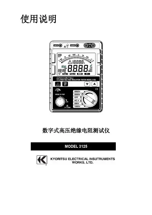
共立6201A中文使用说明书
- 格式:pdf
- 大小:677.15 KB
- 文档页数:17
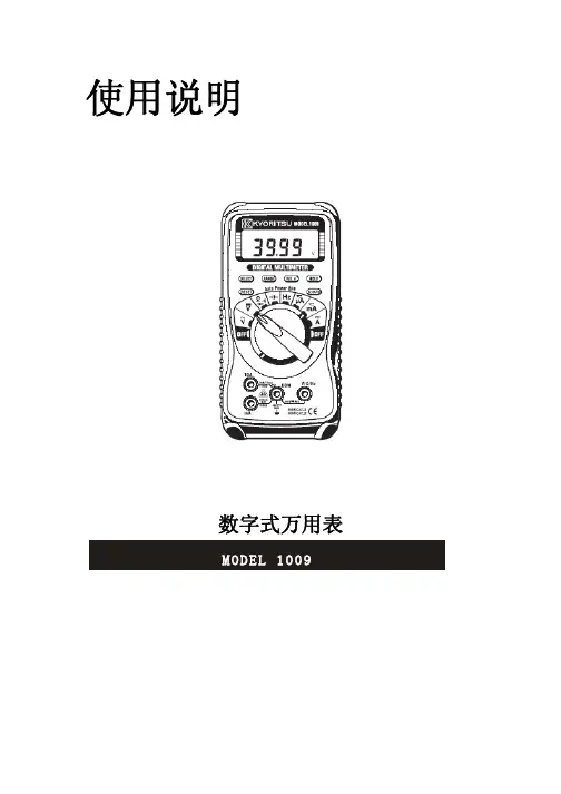
使用说明数字式万用表MODEL 10091.安全警告本仪器根据以下标准进行设计、生产,并且于检查合格后在最好状态下出货。
IEC 61010-1过电压CAT III300V污染度2IEC 61010-031IEC 61326本说明书包含警告和安全规则,记载了避免人身伤害事故和保持仪器能在长期良好状态下使用的注意事项。
因此,使用仪器前请仔细阅读操作指南。
警告● 使用前,通读并理解说明书中的操作指南。
● 请将说明书随身保存以确保可随时参阅。
● 必须由专业工作人员使用并严格遵守使用说明书中的安全指示进行操作。
对任何因错误使用或未遵守使用说明书中记载的注意事项而引起的损伤、人身事故,共立公司概不负责。
● 理解并遵守安全操作指示。
必须严格遵守上述操作说明。
如不遵守,测量时可能会导致人身伤害和仪器毁坏。
仪器上标志,提醒用户在操作时,必须参阅相关操作说明。
标志分为3种,请注意阅读其不同内容。
危险:表示操作不当会导致严重或致命的伤害。
警告:表示操作不当存在导致严重或致命的伤害的可能性。
小心:表示操作不当有可能会导致人身伤害或仪器毁坏。
危险●请勿在对地电压AC300V以上的电路中测量。
●请勿在充满可燃性气体的环境里进行测量。
可能会产生火花引起爆炸。
●测试时,请注意务必使手指位于测试线的安全栅后。
●请勿在仪器表面或手潮湿的情况下使用。
●测量时,请勿打开电池盖。
警告●请勿在非正常情况下进行测量,例如:仪器机体损坏,仪表或测试线金属部件的裸露。
●测试线连接在被测物上时,请勿切换量程开关。
●请勿在仪器上安装替换部件或对仪器进行改造。
如果仪器损坏,请将其返回当地经销商进行检修。
●仪器表面潮湿的情况下,请勿更换电池。
●请将量程开关转到“OFF”并取下测试线后,打开电池盖更换电池。
注意●测量前,请将量程开关转到适当位置。
●请勿将仪表暴露在阳光、高温、潮湿、露水的环境里。
●长期不使用或储藏时,取下电池。
●请勿使用研磨剂或有机溶剂进行清洗,必须使用中性洗剂或湿抹布清洗。
电子书--E读H6201使用手册Ver 28.41您好感谢您选用本公司生产的产品!为了使您尽快轻松自如地操作您的产品,我们随机配备了内容详尽的用户手册,您可以获取有关产品介绍、使用方法等方面的知识。
使用您的产品之前,请仔细阅读我们随机提供的所有资料,以便您能更好地使用该产品。
在编写本手册时我们非常认真和严谨,希望能给您提供完备可靠的信息,然而难免有错误和疏漏之处,请您给予谅解并由衷地欢迎您批评和指正。
如果您在使用该产品的过程中发现什么问题,请及时拨打我们的服务热线,感谢您的支持和合作!请随时备份您的数据资料到您的电脑上。
本公司对于因软件、硬件的误操作、产品维修、电池更换或其它意外情况所引起的个人数据的丢失和损坏不负任何责任,也不对由此而造成的其它间接损失负责。
同时我们无法控制用户对本手册可能造成的误解,因此,本公司将不对在使用本手册过程中可能出现的意外损失负责,并不对因使用该产品而引起的第三方索赔负责。
本手册中的信息如有变更,恕不另行通知。
本手册信息受到版权保护,其任何部分未经本公司事先书面许可,不准以任何方式影印和复制。
本公司保留对本手册、三包凭证及其相关资料的最终解释权。
本产品符合GB/T 18220-2000手持式个人信息处理设备通用规范。
注意事项✧不要在高度潮湿的环境下使用适配器,切勿用湿的手足去碰适配器。
✧切勿用金属物体接触机器,这样容易造成机器短路。
✧建议及时备份存放在本机中的个人资料。
✧请不要试图分解或改造本机,这样可能导致电击或妨碍产品质保。
✧清洁机器时,请使用柔软的布清洁表面。
✧如果表面严重污浊,可用软布占少许清水或柔软清洁剂清洁。
✧请注意不要让液体进入机器内部。
✧禁止儿童单独玩耍本机,请勿摔落或与硬物摩擦撞击,否则可能导致机器表面磨花、硬盘损伤、数据丢失或其它硬件损坏。
✧为保证机器安全,请勿在高温环境下对本机进行充电,如暖气旁、电热毯等环境下;并禁止在充电时将产品或充电器上放置遮盖物,如被子、衣物等。
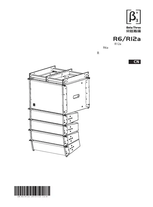
R6/R12a一组共包括一只R12a有源超低音、四只R6a全频扬声器和音箱吊架R系列中型阵列扬声器系统产品说明书CN U M-R6/R12a-20131123v e r B感谢您购买 产品!请仔细阅读本手册,它将帮助你妥善设置并运行您的系统,使其发挥卓越的性能。
并保留这些说明以供日后参照。
警告:为了降低火灾与电击的风险,请不要将产品暴露在雨中或潮湿环境中。
警告:为了降低电击的风险,非专业人士请勿擅自拆卸该系统。
仅供专业人士操作。
等边三角形中的闪电标记,用以警示用户该部件为非绝缘体,系统内部存在着电压危险,电压。
可能足以引起触电。
可能足以引起触电如系统标有带惊叹号的等边三角形,则是为提示用户严格遵守本用户指南中的操作与维护规定。
注意:请勿对系统或附件作擅自的改装。
未经授权擅自改装将造成安全隐患。
警告:燃不得将明火源(如点的蜡烛)放在器材上面。
1. 请先阅读本说明。
2. 保留这些说明以供日后参照。
3. 注意所有警告信息。
4. 遵守各项操作指示。
5. 不要在雨水中或潮湿环境中使用本产品。
6. 不要将产品靠近热源安装,例如暖气管、加热器、火炉或其它能产生热量的装置(包括功放机 )。
7. 不要破坏极性或接地插头的安全性设置。
如果提供的插头不能插入插座,则应当请专业人员更换插座。
8. 保护好电源线和信号线,不要在上面踩踏或拧在一起(尤其是插头插座及穿出机体以外的部分 )。
9. 使用厂商规定及符合当地安全标准的附件。
10.雷电或长时间不使用时请断电以防止损坏产品。
12. 不要让物体或液体落入产品内——它们可能引起火灾或触电。
13. 请注意产品外罩上的相关安全标志。
. 仅与厂商指定或与电器一同售出的推车、架子、三脚架、支架或桌子一起使用。
推动小车/电器时,应谨防翻倒。
11注意事项产品的安装调试须由专业人士操作。
在使用非本厂规定的吊装件时,要保证结构的强度并符合当地的安全规范。
警告:1扬声器及扬声器系统的产品有限保修期为自正式购买日起的3年。

XC6201SeriesPositive Voltage Regulators■GENERAL DESCRIPTIONThe XC6201 series are highly precise, low power consumption, positive voltage regulators manufactured using CMOS and laser trimming technologies.The series provides large currents with a significantly small dropout voltage.The XC6201 consists of a current limiter circuit, a driver transistor, a precision reference voltage and an error amplifier. Output voltage is selectable in 0.1V steps between 1.3V ~ 6.0V.SOT-25, SOT-89, USP-6B and TO-92 packages are available.■APPLICATIONS●Mobile Phones●Cordless phones, wireless communication equipment ●Cameras, video recorders●Portable games●Portable AV equipment●Reference voltage●Battery powered equipment■TYPICAL APPLICATION CIRCUIT ■FEATURESMaximum Output Current: 250mA (TYP.)Dropout Voltage: 0.16V @ 100mA: 0.40V @ 200mAMaximum Operating Voltage :10VOutput Voltage Range: 1.3V ~ 6.0V (0.1V increments) Fixed Voltage Accuracy : ±1% (V OUT(T)>2.0V)±2%Low Power Consumption :2.0μA (TYP.)Operating Ambient Temperature: -40℃ ~ 85℃Packages : SOT-25,SOT-89TO-92USP-6BEnvironmentally Friendly : EU RoHS Compliant, Pb Free Tantalum or Ceramic Capacitor compatible■TYPICAL PERFORMANCE CHARACTERISTICSXC6201P332ETR0301-005●Supply Current vs. Input VoltagePIN NUMBERSOT-25SOT-89/TO-92 (T)USP-6BPIN NAMEFUNCTION5 1 3 V OUT Output 2 2 5 V SS Ground 1 3 1 V IN Power Input 3, 4- 2,4,6 NC No ConnectionDESIGNATORITEM SYMBOLDESCRIPTION① Product Number 01 -② Type of Regulator P 3-pin regulator ③④ Output Voltage 13~60 e.g. 30:3.0V50:5.0V 1 ±1% ⑤Output Voltage Accuracy2±2%MR SOT-25 (3,000/Reel) MR-G SOT-25 (3,000/Reel) PR SOT-89 (1,000/Reel) PR-G SOT-89 (1,000/Reel)TH TO-92Taping Type: Paper type (2,000/Tape)TH-G TO-92 Taping Type: Paper type (2,000/Tape) TB TO-92 Taping Type: Bag (500/Bag) TB-G TO-92 Taping Type: Bag (500/Bag) DR USP-6B (3,000/Reel) ⑥⑦-⑧Packages(Order Unit)DR-G USP-6B (3,000/Reel)■PIN CONFIGURATION ■PIN ASSIGNMENT■PRODUCT CLASSIFICATION●Ordering Information*The dissipation pad for the USP-6B package should be solder-plated in recommended mount pattern and metal masking so as to enhance mounting strength and heat release. If the pad needs to be connected to other pins, it should be connected to the V SS (No.5) pin.NCVSS NCVIN NC VOUTX C 6 2 0 1 P ③④⑤⑥⑦-⑧(*1)① ②(*1)The “-G” suffix denotes Halogen and Antimony free as well as being fully RoHS compliant.* +1% accuracy can be set at V OUT(T) > 2.0V.(SIDE VIEW)XC6201SeriesPARAMETERSYMBOLRATINGSUNITS Input Voltage V IN 12.0 V Output Current I OUT 500 mA Output Voltage V OUT V SS -0.3~V IN +0.3V SOT-25 250 SOT-89 500 TO-92 300 PowerDissipation USP-6B Pd 120mWOperating Temperature Topr -40~+85 ℃Storage Temperature Tstg -55~+125 ℃===■ABSOLUTE MAXIMUM RATINGSTa = 25℃ ■ELECTRICAL CHARACTERISTICSXC6201P132V OUT(T)=1.3V (*1)Ta=25℃■BLOCK DIAGRAM■ELECTRICAL CHARACTERISTICS(Continued)XC6201P182 V OUT(T)=1.8V (*1)Ta=25℃V OUT(T)=2.7V (*1)XC6201Series■ELECTRICAL CHARACTERISTICS(Continued)XC6201P332 V OUT(T)=3.3V (*1)Ta=25℃V OUT(T)=5.0V (*1)NOTE:*1: V OUT(T) = Nominal output voltage.*2: V OUT(E) = Effective output voltage (i.e. the output voltage when “V OUT(T)+1.0V” is provided whilemaintaining a certain I OUT value).*3: Vdif = (V IN1- V OUT1)V IN1 :An Input Voltage when V OUT1 appears as the input voltage is gradually decreased.V OUT1 : A voltage equal to 98% of the output voltage when a stabilized (V OUT(T) + 1.0V) is input.■TYPICAL APPLICATION CIRCUIT(Tantalum) (Tantalum)With the XC6201 series regulator, in order to ensure the stabilized output voltage, we suggest that an output capacitor (C L) of 1μF or more be connected between the output pin (V OUT) and the V SS pin. For using low ESR capacitor (e.g. ceramic capacitors), please make sure that the output voltage is more than 1.7V. When the output voltage is from 1.3V to 1.6V, the output capacitor should be a tantalum capacitor with a capacitance of 2.2μF. We also suggest an input capacitor (C IN) should be connected between the V IN and the V SS in order to stabilize input power source.OUTPUT VOLTAGE C IN C L (TANTALUM) C L (LOW ESR)1.3V~1.6V ≧1.0μF ≧2.2μF -1.7V~6.0V ≧1.0μF ≧1.0μF ≧1.0μFV IN=1.8V~10V,V OUT=1.7~6.0VC IN=1.0μF(Ceramic),C L=1.0μF(ceramic)XC6201Series1. Please use this IC within the stated absolute maximum ratings. The IC is liable to malfunction should the ratings be exceeded. When a voltage higher than the V IN flows to the V OUT like when using two power supplies, please connect a Schottky barrier diode between the V OUT and the V IN and do not exceed the V OUT rating.2. An oscillation may occur by the impedance between a power supply and the input of the IC. Where the impedance is 10Ωor more, please use an input capacitor (C IN ) of at least 1μF. In case of high output current, operation can be stabilized by increasing the input capacitor value. Also an oscillation may occur if the input capacitor value is smaller than the input impedance when the output capacitance (C L ) is large. In such cases, operations can be stabilized by either increasing the input capacitor value or reducing the output capacitor value.3. Please ensure that output current (I OUT ) is less than Pd / (V IN - V OUT ) and do not exceed the rated power dissipation value (Pd) of the package.Circuit ① : Supply Current■TEST CIRCUITSCircuit ② : Output Voltage, Oscillation, Line Regulation, Dropout Voltage, Load Regulation■ NOTE ON USE■TYPICAL PERFORMANCE CHARACTERISTICS(1) Output Voltage vs. Output CurrentXC6201Series■TYPICAL PERFORMANCE CHARACTERISTICS (Continued)(2) Output Voltage vs. Input VoltageXC6201P132 XC6201P132XC6201P182XC6201P182XC6201P272 XC6201P272■TYPICAL PERFORMANCE CHARACTERISTICS (Continued) (2) Output Voltage vs. Input Voltage (Continued)XC6201P332 XC6201P332XC6201P502 XC6201P502Series ■TYPICAL PERFORMANCE CHARACTERISTICS (Continued)(3) Dropout Voltage vs. Output CurrentXC6201P132 XC6201P182XC6201P272 XC6201P332XC6201P502(4) Supply Current vs. Input Voltage ■TYPICAL PERFORMANCE CHARACTERISTICS (Continued) XC6201P132 XC6201P132 XC6201P182Series(4) Supply Current vs. Input Voltage (Continued) ■TYPICAL PERFORMANCE CHARACTERISTICS (Continued) XC6201P332(5) Output Voltage vs. Ambient Temperature■TYPICAL PERFORMANCE CHARACTERISTICS (Continued)Series(6) Supply Current vs. Ambient Temperature■TYPICAL PERFORMANCE CHARACTERISTICS (Continued)■TYPICAL PERFORMANCE CHARACTERISTICS (Continued) (7) Input Transient ResponseXC6201P132 XC6201P182Time (1ms/div) Time (1ms/div)XC6201P272 XC6201P332Time (1ms/div) Time (1ms/div)XC6201P502Time (1ms/div)Series■TYPICAL PERFORMANCE CHARACTERISTICS (Continued)(8) Load Transient ResponseXC6201P132 XC6201P182Time (2ms/div) Time (2ms/div)XC6201P272 XC6201P332Time (2ms/div) Time (2ms/div)XC6201P502Time (2ms/div)(9) Ripple Rejection Rate (10) Output Noise Density ■TYPICAL PERFORMANCE CHARACTERISTICS (Continued)XC6201P132 XC6201P182 XC6201P272 XC6201P332 XC6201P502XC6201P502 XC6201P302Series■PACKAGING INFORMATION ●SOT-25 ●SOT-89Unit : mm Unit : mmPapertype Bag●USP-6B ■PACKAGING INFORMATION (Continued)●TO-92Unit : mm Unit : mm Unit : mm■PACKAGING INFORMATION(Continued)●USP-6B Reference Pattern Layout ●USP-6B Reference Metal Mask DesignMARKPRODUCT SERIES1 XC6201xxxxxxMARKVoltage= 0.1 ~ 3.0V Voltage= 3.1 ~ 6.0VPRODUCT SERIES5 6 XC6201PXXXXX 8 9 XC6201TXXXPXMARK OUTPUT VOLTAGE (V) MARK OUTPUT VOLTAGE (V)0 - 3.1 - F 1.6 4.6 - 1 - 3.2 - H 1.7 4.7 - 2 - 3.3 - K 1.8 4.8 - 3 - 3.4 - L 1.9 4.9 - 4 - 3.5 - M 2.0 5.0 - 5 - 3.6 - N 2.1 5.1 - 6 - 3.7 - P 2.2 5.2 - 7 - 3.8 - R 2.3 5.3 - 8 - 3.9 - S 2.4 5.4 - 9 - 4.0 - T 2.5 5.5 - A - 4.1 - U 2.6 5.6 - B-4.2-V 2.7 5.7 - C 1.3 4.3 - X 2.8 5.8 - D 1.4 4.4 - Y 2.9 5.9 - E 1.5 4.5 -Z 3.0 6.0 -■MARKING RULE●SOT-89, SOT-25① represents the product series② represents type of regulator③ represents output voltage④ represents assembly lot number0 to 9, A to Z repeated (G, I, J, O, Q, W excluded)④③②①123SOT-89 (TOP VIEW)①②③④12354SOT-25(TOP VIEW)MARKPRODUCT SERIESP XC6201Pxxxxx T XC6201TxxxxxMARK ②③VOLTAGE (V)PRODUCT SERIES 3 3 3.3 XC6201Px33xx 5 05.0XC6201Px50xxMARK DETECT VOLTAGE ACCURACYPRODUCT SERIES 1 Within ±1% XC6201Pxx1xx 2Within ±2%XC6201Pxx2xxMARKPRODUCTION YEAR3 20034 2004MARK①②PRODUCT SERIES0 1XC6201xxxxDxMARKTYPEPRODUCT SERIESP 3pin Regulator XC6201PxxxDx T V IN =7V(Rated)XC6201TxxxDxMARK ④⑤VOLTAGE (V)PRODUCT SERIES3 3 3.3 XC6201x33xDx 5 0 5.0 XC6201x50xDx●TO-92① represents type of regulator⑤ represents least significant digit of production year②③ represents output voltage④ represents detect voltage accuracy⑥ represents the production lot number0 to 9, A to Z repeated (G, I, J, O, Q, W excluded) Note: No character inversion used.●USP-6B①② represents product series③ represents type of regulator④⑤ represents output voltage■MARKING RULE (Continued)USP-6B (TOP VIEW)⑥ represents assembly lot number0 to 9, A to Z repeated (G, I, J, O, Q, W excluded) Note: No character inversion used.(SIDE VIEW)。
User's GuideSLVU458–April2011TPS7A6201QKTT EVMContents1Introduction (2)2Setup (2)2.1Input/Output Connector Description (2)2.2Setup (2)2.3Operation (2)3Board Layout (3)4Schematic and Bill of Materials (5)4.1Schematic (5)4.2Bill of Materials (5)List of Figures1Enable Jumper (2)2Top Assembly Layer (3)3Top Layer Routing (4)4Bottom Assembly Layer (4)5TPS7A6201QKTT EVM Schematic (5)List of Tables1Device and Package Configurations (2)2TPS7A6201QKTT EVM Bill of Materials (5)PowerPAD is a trademark of Texas Instruments.1 SLVU458–April2011TPS7A6201QKTT EVM Submit Documentation FeedbackENdeviceenabledENdevicedisabledR1VOUT =1.23x 1+R2æö÷ç÷ç÷çèøIntroduction 1IntroductionThe Texas Instruments TPS7A6201QKTT EVM evaluation module (EVM)helps designers evaluate the operation and performance of the TPS7A6201QKTT Linear Regulator.The EVM contains one linear regulator (see Table 1).Table 1.Device and Package ConfigurationsConverterICPackage U1TPS7A6201QKTTRQ1KTT-52SetupThis section describes the jumpers and connectors on the EVM as well and how to properly connect,set up and use the TPS7A6201QKTT EVM.2.1Input/Output Connector DescriptionVBAT is the protected power input for the regulator.The test point provides a power (Vbat)connection and a reverse battery protection diode to allow the user to power the EVM.GND is the ground return for the regulator.The EVM provides three GND test points to allow the user to power the EVM,connect the load and attach an oscilloscope ground leadVIN is a power test point.The test point allows the user to measure the input voltage after the reverse battery protection diode.The user can also apply power to the regulator through this test point.VOUT is output for the regulator.The test point provides a connection to attach a load to the EVM.EN is a test point to monitor the Enable input to the device.It can also be used to provide an enable signal to the device from an outside source,if the EN jumper is left open.The EN jumper will disable the regulator when removed and enable the regulator when installed.Figure 1.Enable JumperFB is a test point to monitor the feedback voltage to the device.The EVM is setup to provide a 5V output voltage,but the feedback resistors can be changed to set the output voltage to a value between 2.5V and 7V using the equation presented in Equation 1.(1)2.2SetupThe input voltage range for the converter is (VOUT +0.3V)volts to 40volts.The EVM can support up to 300mA of load current.2.3OperationThe TPS7A6201QKTT will power-up after the VBAT voltage has exceeded the Power-On Reset threshold.In this configuration,the device will power up when power is applied.The PCB offers footprints for the TPS7A6201QKTTQ1or the TPS7A6201QKVUQ1device.2TPS7A6201QKTT EVMSLVU458–April 2011Submit Documentation Feedback Board Layout 3Board LayoutFigure2,through Figure4show the board layout for the TPS7A6201QKTT EVM PWB.The PowerPAD™package offers an exposed thermal pad to enhance thermal performance.This must be soldered to the copper landing on the PCB for optimal performance.The PCB provides2oz copperplanes on the top and bottom to dissipate heat.SpacerFigure2.Top Assembly Layer3 SLVU458–April2011TPS7A6201QKTT EVM Submit Documentation FeedbackBoard Layout Figure3.Top Layer RoutingFigure4.Bottom Assembly Layer4TPS7A6201QKTT EVM SLVU458–April2011Submit Documentation FeedbackEvaluation Board/Kit Important NoticeTexas Instruments(TI)provides the enclosed product(s)under the following conditions:This evaluation board/kit is intended for use for ENGINEERING DEVELOPMENT,DEMONSTRATION,OR EVALUATION PURPOSES ONLY and is not considered by TI to be a finished end-product fit for general consumer use.Persons handling the product(s)must have electronics training and observe good engineering practice standards.As such,the goods being provided are not intended to be complete in terms of required design-,marketing-,and/or manufacturing-related protective considerations, including product safety and environmental measures typically found in end products that incorporate such semiconductor components or circuit boards.This evaluation board/kit does not fall within the scope of the European Union directives regarding electromagnetic compatibility,restricted substances(RoHS),recycling(WEEE),FCC,CE or UL,and therefore may not meet the technical requirements of these directives or other related directives.Should this evaluation board/kit not meet the specifications indicated in the User’s Guide,the board/kit may be returned within30 days from the date of delivery for a full refund.THE FOREGOING WARRANTY IS THE EXCLUSIVE WARRANTY MADE BY SELLER TO BUYER AND IS IN LIEU OF ALL OTHER WARRANTIES,EXPRESSED,IMPLIED,OR STATUTORY,INCLUDING ANY WARRANTY OF MERCHANTABILITY OR FITNESS FOR ANY PARTICULAR PURPOSE.The user assumes all responsibility and liability for proper and safe handling of the goods.Further,the user indemnifies TI from all claims arising from the handling or use of the goods.Due to the open construction of the product,it is the user’s responsibility to take any and all appropriate precautions with regard to electrostatic discharge.EXCEPT TO THE EXTENT OF THE INDEMNITY SET FORTH ABOVE,NEITHER PARTY SHALL BE LIABLE TO THE OTHER FOR ANY INDIRECT,SPECIAL,INCIDENTAL,OR CONSEQUENTIAL DAMAGES.TI currently deals with a variety of customers for products,and therefore our arrangement with the user is not exclusive.TI assumes no liability for applications assistance,customer product design,software performance,or infringement of patents or services described herein.Please read the User’s Guide and,specifically,the Warnings and Restrictions notice in the User’s Guide prior to handling the product.This notice contains important safety information about temperatures and voltages.For additional information on TI’s environmental and/or safety programs,please contact the TI application engineer or visit /esh.No license is granted under any patent right or other intellectual property right of TI covering or relating to any machine,process,or combination in which such TI products or services might be or are used.FCC WarningThis evaluation board/kit is intended for use for ENGINEERING DEVELOPMENT,DEMONSTRATION,OR EVALUATION PURPOSES ONLY and is not considered by TI to be a finished end-product fit for general consumer use.It generates,uses,and can radiate radio frequency energy and has not been tested for compliance with the limits of computing devices pursuant to part15 of FCC rules,which are designed to provide reasonable protection against radio frequency interference.Operation of this equipment in other environments may cause interference with radio communications,in which case the user at his own expense will be required to take whatever measures may be required to correct this interference.EVM Warnings and RestrictionsIt is important to operate this EVM within the input voltage range of2V to40V(Boost enabled)or4V to40V(Boost disabled)and the output voltage range of9V to11V.Exceeding the specified input range may cause unexpected operation and/or irreversible damage to the EVM.If there are questions concerning the input range,please contact a TI field representative prior to connecting the input power.Applying loads outside of the specified output range may result in unintended operation and/or possible permanent damage to the EVM.Please consult the EVM User's Guide prior to connecting any load to the EVM output.If there is uncertainty as to the load specification,please contact a TI field representative.During normal operation,some circuit components may have case temperatures greater than85°C.The EVM is designed to operate properly with certain components above60°C as long as the input and output ranges are maintained.These components include but are not limited to linear regulators,switching transistors,pass transistors,and current sense resistors.These types of devices can be identified using the EVM schematic located in the EVM User's Guide.When placing measurement probes near these devices during operation,please be aware that these devices may be very warm to the touch.Mailing Address:Texas Instruments,Post Office Box655303,Dallas,Texas75265Copyright©2011,Texas Instruments IncorporatedIMPORTANT NOTICETexas Instruments Incorporated and its subsidiaries(TI)reserve the right to make corrections,modifications,enhancements,improvements, and other changes to its products and services at any time and to discontinue any product or service without notice.Customers should obtain the latest relevant information before placing orders and should verify that such information is current and complete.All products are sold subject to TI’s terms and conditions of sale supplied at the time of order acknowledgment.TI warrants performance of its hardware products to the specifications applicable at the time of sale in accordance with TI’s standard warranty.Testing and other quality control techniques are used to the extent TI deems necessary to support this warranty.Except where mandated by government requirements,testing of all parameters of each product is not necessarily performed.TI assumes no liability for applications assistance or customer product design.Customers are responsible for their products and applications using TI components.To minimize the risks associated with customer products and applications,customers should provide adequate design and operating safeguards.TI does not warrant or represent that any license,either express or implied,is granted under any TI patent right,copyright,mask work right, or other TI intellectual property right relating to any combination,machine,or process in which TI products or services are rmation published by TI regarding third-party products or services does not constitute a license from TI to use such products or services or a warranty or endorsement e of such information may require a license from a third party under the patents or other intellectual property of the third party,or a license from TI under the patents or other intellectual property of TI.Reproduction of TI information in TI data books or data sheets is permissible only if reproduction is without alteration and is accompanied by all associated warranties,conditions,limitations,and notices.Reproduction of this information with alteration is an unfair and deceptive business practice.TI is not responsible or liable for such altered rmation of third parties may be subject to additional restrictions.Resale of TI products or services with statements different from or beyond the parameters stated by TI for that product or service voids all express and any implied warranties for the associated TI product or service and is an unfair and deceptive business practice.TI is not responsible or liable for any such statements.TI products are not authorized for use in safety-critical applications(such as life support)where a failure of the TI product would reasonably be expected to cause severe personal injury or death,unless officers of the parties have executed an agreement specifically governing such use.Buyers represent that they have all necessary expertise in the safety and regulatory ramifications of their applications,and acknowledge and agree that they are solely responsible for all legal,regulatory and safety-related requirements concerning their products and any use of TI products in such safety-critical applications,notwithstanding any applications-related information or support that may be provided by TI.Further,Buyers must fully indemnify TI and its representatives against any damages arising out of the use of TI products in such safety-critical applications.TI products are neither designed nor intended for use in military/aerospace applications or environments unless the TI products are specifically designated by TI as military-grade or"enhanced plastic."Only products designated by TI as military-grade meet military specifications.Buyers acknowledge and agree that any such use of TI products which TI has not designated as military-grade is solely at the Buyer's risk,and that they are solely responsible for compliance with all legal and regulatory requirements in connection with such use. TI products are neither designed nor intended for use in automotive applications or environments unless the specific TI products are designated by TI as compliant with ISO/TS16949requirements.Buyers acknowledge and agree that,if they use any non-designated products in automotive applications,TI will not be responsible for any failure to meet such requirements.Following are URLs where you can obtain information on other Texas Instruments products and application solutions:Products ApplicationsAudio /audio Communications and Telecom /communicationsAmplifiers Computers and Peripherals /computersData Converters Consumer Electronics /consumer-appsDLP®Products Energy and Lighting /energyDSP Industrial /industrialClocks and Timers /clocks Medical /medicalInterface Security /securityLogic Space,Avionics and Defense /space-avionics-defense Power Mgmt Transportation and /automotiveAutomotiveMicrocontrollers Video and Imaging /videoRFID Wireless /wireless-appsRF/IF and ZigBee®Solutions /lprfTI E2E Community Home Page Mailing Address:Texas Instruments,Post Office Box655303,Dallas,Texas75265Copyright©2011,Texas Instruments Incorporated。
DATA-6201无线抄表终端使用说明书唐山平升电子技术开发有限公司售前咨询:************地址:河北省唐山市高新技术开发区庆北道37号网址:版权声明:本使用说明书包含的所有内容均受版权法的保护,未经唐山平升电子技术开发有限公司的书面授权,任何组织和个人不得以任何形式或手段对整个说明书和部分内容进行复制和转载,并不得以任何形式传播。
商标声明:为唐山平升电子技术开发有限公司的注册商标。
本文档提及的其他所有商标或注册商标,由拥有该商标的机构所有。
注意:由于产品版本升级或其他原因,本文档内容会不定期进行更新。
除非另有约定,本文档仅作为使用指导,本文档中的所有陈述、信息和建议不构成任何明示或暗示的担保。
目录第一章产品简介 (1)1.1概述 (1)1.2产品特点 (1)1.3产品功能 (1)1.4产品结构 (2)1.5技术参数 (4)1.6出厂配置 (4)第二章设备安装与维护 (5)2.1产品关机与开机 (5)2.2配件安装 (5)2.2.1航插安装 (5)2.2.3支架的安装 (6)2.3仪表接线说明 (6)2.3电池拆卸与安装 (7)第三章手机APP的使用 (8)3.1手机APP工具软件 (8)3.1.1手机APP软件安装 (8)3.1.2手机APP软件应用 (8)第四章故障分析与排除 (13)第一章产品简介1.1概述DATA-6201无线抄表终端为各类仪表增加远传功能提供智慧解决方案,通过RS485接口可便捷对接各类水表、水位计等仪表,实现数据采集并通过4G/NB-IoT无线远传至中心服务器,既不改变原有仪表安装,又能实现仪表数据的远传功能。
1.2产品特点●内嵌程序支持上百种流量计、水位计选择及标准Modbus协议配置。
●微功耗设计,支持产品关机,延长电池使用寿命。
●防护等级IP68,水中浸泡,依旧工作正常。
●结构紧凑、尺寸小巧,安装简便。
●便捷更换SIM卡、电池。
1.3产品功能●通讯功能:支持通过4G或NB-IoT与多中心进行数据通信。
Dell PowerEdge M620 Systems(适用于 Dell PowerEdge VRTX 机柜)用户手册管制型号: HHB管制类型: HHB003注、小心和警告注: “注”表示可以帮助您更好地使用计算机的重要信息。
小心: “小心”表示可能会损坏硬件或导致数据丢失,并说明如何避免此类问题。
警告: “警告”表示可能会造成财产损失、人身伤害甚至死亡。
版权所有© 2014 Dell Inc. 保留所有权利。
本产品受美国、国际版权和知识产权法律保护。
Dell™和 Dell 徽标是 Dell Inc. 在美国和 / 或其他管辖区域的商标。
所有此处提及的其他商标和产品名称可能是其各自所属公司的商标。
2014–10Rev. A01目录1 关于系统 (7)简介 (7)前面板部件和指示灯 (8)使用 USB 软盘或 USB DVD/CD 驱动器 (8)硬盘驱动器功能部件 (8)您可能需要的其他信息 (9)2 使用系统设置程序和引导管理器 (11)选择系统引导模式 (12)进入系统设置 (12)响应错误消息 (12)使用系统设置程序导航键 (12)系统设置选项 (12)系统设置程序主屏幕 (13)系统 BIOS 屏幕 (13)System Information(系统信息)屏幕 (14)Memory Settings(内存设置)屏幕 (14)Processor Settings(处理器设置)屏幕 (15)SATA Settings(SATA 设置)屏幕 (16)Boot Settings(引导设置)屏幕 (16)Integrated Devices(集成设备)屏幕 (17)Serial Communications(串行通信)屏幕 (18)系统配置文件设置屏幕 (18)System Security(系统安全)屏幕 (19)Miscellaneous Settings(其它设置) (20)系统和设置密码功能 (21)分配系统密码和/或设置密码 (21)使用系统密码保护系统安全 (22)删除或更改现有系统密码和/或设置密码 (22)在已启用设置密码的情况下进行操作 (22)进入 UEFI 引导管理器 (23)使用引导管理器导航键 (23)Boot Manager(引导管理器)屏幕 (23)UEFI Boot(UEFI 引导)菜单 (24)嵌入式系统管理 (24)iDRAC 设置公用程序 (24)进入 iDRAC 设置公用程序 (25)3 安装服务器模块组件 (26)建议工具 (26)安装和卸下服务器模块 (26)卸下服务器模块 (26)安装服务器模块 (28)打开与合上服务器模块 (28)打开服务器模块 (28)合上服务器模块 (29)服务器模块内部 (30)冷却导流罩 (30)卸下冷却导流罩 (30)安装冷却导流罩 (31)系统内存 (31)一般内存模块安装原则 (33)模式特定原则 (34)内存配置示例 (35)卸下内存模块 (38)安装内存模块 (39)PCIe 夹层卡 (40)卸下 PCIe 夹层卡 (40)安装 PCIe 夹层卡 (41)管理提升卡 (42)更换 SD 卡 (42)内部 USB 盘 (43)SD vFlash 卡 (43)装回 SD vFlash 卡 (43)网络子卡/LOM 提升卡 (44)卸下网络子卡/LOM 提升卡 (44)安装网络子卡/LOM 提升卡 (45)处理器 (45)卸下处理器 (46)安装处理器 (48)硬盘驱动器 (49)硬盘驱动器/SSD 安装原则 (50)卸下硬盘驱动器/SSD (50)安装硬盘驱动器/SSD (50)进行硬盘驱动器维修前的关机程序 (51)配置引导驱动器 (51)从硬盘驱动器/SSD 托盘中卸下硬盘驱动器/SSD (51)将硬盘驱动器/SSD 安装到硬盘驱动器/SSD 托盘中 (52)硬盘驱动器/SSD 背板 (52)卸下硬盘驱动器/SSD 背板 (52)安装硬盘驱动器/SSD 背板 (53)系统板 (54)卸下系统板 (54)安装系统板 (55)NVRAM 备用电池 (56)更换 NVRAM 备用电池 (56)存储控制器卡 (57)卸下存储控制器卡 (57)安装存储控制器卡 (58)4 系统故障排除 (59)安全第一—为您和您的系统着想 (59)系统内存故障排除 (59)硬盘驱动器故障排除 (59)USB 设备故障排除 (60)内部 SD 卡故障排除 (60)处理器故障排除 (61)系统板故障排除 (61)NVRAM 备用电池故障排除 (61)5 使用系统诊断程序 (63)Dell Online Diagnostics (63)Dell 嵌入式系统诊断程序 (63)何时使用 Embedded System Diagnostics(嵌入式系统诊断程序) (63)运行嵌入式系统诊断程序 (63)从外部介质运行嵌入式系统诊断程序 (64)系统诊断程序控件 (64)6 跳线和连接器 (65)系统板跳线设置 (65)系统板连接器 (66)禁用已忘记的密码 (67)7 技术规格 (68)8 系统消息 (71)LCD 状态信息 (71)查看 LCD 信息 (71)删除 LCD 消息 (71)系统错误消息 (71)警告信息 (141)诊断消息 (142)警报消息 (142)9 获得帮助 (143)联系 Dell (143)1关于系统简介本说明文件提供了有关 Dell PowerEdge M620 服务器模块的信息,该模块专为 PowerEdge VRTX 机柜配置,并且可以通过服务器模块上的标记为PCIe的标签来进行识别。
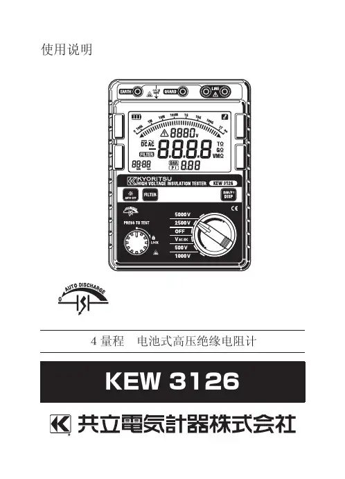
使用说明书多功能测试仪MODEL 6020/6030目录1. 安全警告2. 特点3. 规格4. 仪器布局5. 测试前准备工作6. 测量方法6.1 AC电压测量6.2 绝缘电阻测量6.3. 接地电阻测量6.4. 相位测量6.5. 照明使用方法6.6. 导线卷轴使用方法6.7. 自动关机6.8. 肩腰带使用方法7. 电池更换8.要求维修服务前的注意事项1 .安全警告设计符合安全规格IEC 1010,过电压 CAT II。
本说明书包括警告和安全规格,必须严格遵守以确保安全操作。
因此,使用前请务必通读操作指示。
仪器上的 标志提醒用户必须遵守说明书中相关指示以确保仪器安全操作。
请务必注意仪器上的所有警告和注意事项。
警告事项提醒用户避免触电事故,注意事项则避免仪器损害。
1. 测量前请确保量程开关调节在适当位置。
2. 请务必确保测试线完全插入仪器端口。
3. 仪器潮湿时请勿连接测试线。
4. 测量时的输入值请勿超量程范围。
5. 测试线连接被测回路时请勿切换量程。
6. 请确认仪器和接地间的对地电压低于600V。
7. 请勿在易燃环境中测量。
(例:易燃性气体或火花、蒸气、灰尘处)可能会引起爆炸。
8. 每次使用前请检查仪器、测试线、附件等是否存在危险或异常现象。
若存在异常情况(例:测试线断裂,仪器外壳龟裂)请勿测量。
9. 打开电池盖更换电池时请确认已关闭电源并取下测试线。
10. 仪器潮湿时请勿更换电池。
11. 使用后请关闭电源。
12. 请勿将仪器暴露在阳光直射、潮湿及高温环境中。
13. 请勿在50℃以上环境中使用。
14. 必须由专业工程师对仪器进行校准和修理。
除非有其他能进行急修的人员在现场,否则请勿尝试校准或修理。
15. 请勿随意更换仪器部件。
为确保仪器安全请将仪器返还销售商或修理中心维修。
16. 必须由专业人员严格按照指示操作。
对任何因错误使用或未遵守指示造成的仪器损害和人身事故,共立公司概不负责。
因此,请通读并理解说明书中内容并在使用时严格遵守。