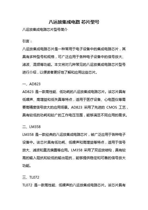
Si823x
- 格式:pdf
- 大小:375.52 KB
- 文档页数:22
Preliminary Rev. 0.11 5/08Copyright © 2008 by Silicon Laboratories Si823xThis information applies to a product under development. Its characteristics and specifications are subject to change without notice.Si823x0.5 AND 4.0A ISO DRIVERSFeaturesApplicationsDescriptionThe Si823x isolated driver family combines two independent, isolated drivers into a single package. The Si8230/1/3/4 are high-side/low-side drivers, and the Si8232/5 are dual low-side drivers. Versions with peak output currents of 0.5A (Si8230/1/2) and 4.0A (Si8233/4/5) are available.All drivers operate with a maximum supply voltage of 24V.These drivers utilize Silicon Labs' proprietary silicon isolation technology,which provides 600V dc (2.5kV acRMS ) withstand voltage per UL1577,and fast 50ns propagation times. Driver outputs can be grounded to the same or separate grounds or connected to a positive or negative voltage.The TTL level compatible inputs are available in individual control input (Si8230/2/3/5) or PWM input (Si8231/4) configurations.High integration, low propagation delay, small installed size, flexibility, and cost-effectiveness make the Si823x family ideal for a wide range of isolated MOSFET/IGBT gate drive applications.Block DiagramsTwo completely isolated drivers in one package 2.5kV RMS output-to-input differential voltage600VDC peak driver-to-driver differential voltage HS/LS and dual LS versions Up to 8MHz switching frequency 0.5A peak output (Si8230/1/2), 4.0A peak output (Si8233/4/5) Independent HS and LS inputs or PWM input versions Common-mode transientimmunity >35kV/µs Overlap protection and programmable dead time (Si8230/1/3/4) Operating temperature range –40 to +125°CUL/VDE/CSA approval (pending)Power delivery systems Motor control systemsLighting control systems Plasma displaysPatents pendingSi823x2Preliminary Rev. 0.11Si823xPreliminary Rev. 0.113T ABLE OF C ONTENTSSectionPage1. Top-Level Block Diagrams . . . . . . . . . . . . . . . . . . . . . . . . . . . . . . . . . . . . . . . . . . . . . . . . .42. Pin Descriptions . . . . . . . . . . . . . . . . . . . . . . . . . . . . . . . . . . . . . . . . . . . . . . . . . . . . . . . . . .63. Electrical Specifications . . . . . . . . . . . . . . . . . . . . . . . . . . . . . . . . . . . . . . . . . . . . . . . . . . .83.1. Test Circuits . . . . . . . . . . . . . . . . . . . . . . . . . . . . . . . . . . . . . . . . . . . . . . . . . . . . . . .104. Overview . . . . . . . . . . . . . . . . . . . . . . . . . . . . . . . . . . . . . . . . . . . . . . . . . . . . . . . . . . . . . . .125. Application Information . . . . . . . . . . . . . . . . . . . . . . . . . . . . . . . . . . . . . . . . . . . . . . . . . . .135.1. Products . . . . . . . . . . . . . . . . . . . . . . . . . . . . . . . . . . . . . . . . . . . . . . . . . . . . . . . . . .135.2. Device Behavior . . . . . . . . . . . . . . . . . . . . . . . . . . . . . . . . . . . . . . . . . . . . . . . . . . . .135.3. Power Supply Connections . . . . . . . . . . . . . . . . . . . . . . . . . . . . . . . . . . . . . . . . . . . .145.4. Power Dissipation Considerations . . . . . . . . . . . . . . . . . . . . . . . . . . . . . . . . . . . . . .145.5. Layout Considerations . . . . . . . . . . . . . . . . . . . . . . . . . . . . . . . . . . . . . . . . . . . . . . .155.6. Device Operation . . . . . . . . . . . . . . . . . . . . . . . . . . . . . . . . . . . . . . . . . . . . . . . . . . .155.7. Programmable Dead Time and Overlap Protection . . . . . . . . . . . . . . . . . . . . . . . . .166. Applications . . . . . . . . . . . . . . . . . . . . . . . . . . . . . . . . . . . . . . . . . . . . . . . . . . . . . . . . . . . .186.1. High-Side/Low-Side Driver . . . . . . . . . . . . . . . . . . . . . . . . . . . . . . . . . . . . . . . . . . . .186.2. Dual Low-Side Driver . . . . . . . . . . . . . . . . . . . . . . . . . . . . . . . . . . . . . . . . . . . . . . . .197. Ordering Guide . . . . . . . . . . . . . . . . . . . . . . . . . . . . . . . . . . . . . . . . . . . . . . . . . . . . . . . . . .208. Package Outline: Wide Body SOIC . . . . . . . . . . . . . . . . . . . . . . . . . . . . . . . . . . . . . . . . . .21Contact Information . . . . . . . . . . . . . . . . . . . . . . . . . . . . . . . . . . . . . . . . . . . . . . . . . . . . . . . .22Si823x4Preliminary Rev. 0.111. Top-Level Block DiagramsFigure 1.Si8230/3 Two-Input High-Side/Low-Side Isolated DriversFigure 2.Si8231/4 Single-Input High-Side/Low-Side Isolated DriversSi823xPreliminary Rev. 0.115Figure 3.Si8232/5 Dual Low-Side Isolated DriversSi823x6Preliminary Rev. 0.112. Pin DescriptionsTable 1. Si8230/3 Two-Input HS/LS Isolated DriverPin Name Description1VIA Non-inverting logic input terminal for Driver A.2VIB Non-inverting logic input terminal for Driver B.3VDDI Input-side power supply terminal; connect to a source of 4.5 to 5.5V.4GNDI Input-side ground terminal5DISABLE Device Disable. When high, this input unconditionally drives outputs VOA, VOB LOW. It is strongly recommended that this input be connected to external logic level to avoid erroneousoperation due to capacitive noise coupling.6DT Dead time programming input. The value of the resistor connected from DT to ground sets the dead time between output transitions of VOA and VOB. Defaults to 7ns dead time when con-nected to VDDI or left open (see "5.7.Programmable Dead Time and Overlap Protection" onpage 16).7NC No connection.8VDDI Input-side power supply terminal; connect to a source of 4.5 to 5.5V.9GNDB Ground terminal for Driver B.10VOB Driver B output (low-side driver).11VDDB Driver B power supply voltage terminal; connect to a source of 10 to 24V.12NC No connection.13NC No connection.14GNDA Ground terminal for Driver A.15VOA Driver A output (high-side driver).16VDDA Driver A power supply voltage terminal; connect to a source of 10 to 24V.Table 2. Si8231/4 PWM Input HS/LS Isolated DriverPin Name Description1PWM PWM input2NC No connection.3VDDI Input-side power supply terminal; connect to a source of 4.5 to 5.5V.4GNDI Input-side ground terminal.5DISABLE Device Disable. When high, this input unconditionally drives outputs VOA, VOB LOW. It is strongly recommended that this input be connected to external logic level to avoid erroneousoperation due to capacitive noise coupling.6DT Dead time programming input. The value of the resistor connected from DT to ground sets the dead time between output transitions of VOA and VOB. Defaults to 7ns dead time when con-nected to VDDI or left open (see "5.7.Programmable Dead Time and Overlap Protection" onpage 16).7NC No connection.Si823xPreliminary Rev. 0.1178VDDI Input-side power supply terminal; connect to a source of 4.5 to 5.5 V.9GNDB Ground terminal for VOB driver output.10VOB Driver B output (low-side driver).11VDDB Driver B power supply voltage terminal; connect to a source of 10 to 24V.12NC No connection.13NC No connection.14GNDA Ground terminal for Driver A.15VOA Driver A output (high-side driver).16VDDADriver A power supply voltage terminal; connect to a source of 10 to 24V.Table 3. Si8232/5 Dual LS Isolated DriverPin Name Description1VIA Non-inverting logic input terminal for Driver A.2VIB Non-inverting logic input terminal for Driver B.3VDDI Input-side power supply terminal; connect to a source of 4.5 to 5.5V.4GNDIInput-side ground terminal.5DISABLE Device Disable. When high, this input unconditionally drives outputs VOA, VOB LOW. It isstrongly recommended that this input be connected to external logic level to avoid erroneous operation due to capacitive noise coupling.6NC No connection.7NC No connection.8VDDI Input-side power supply terminal; connect to a source of 4.5 to 5.5V.9GNDB Ground terminal for VOB driver output.10VOB Driver B output.11VDDB Driver output VOB power supply voltage terminal; connect to a source of 10 to 24V.12NC No connection.13NC No connection.14GNDA Ground terminal for Driver A.15VOA Driver B output.16VDDADriver A power supply voltage terminal; connect to a source of 10 to 24V.Table 2. Si8231/4 PWM Input HS/LS Isolated Driver (Continued)Si823x8Preliminary Rev. 0.113. Electrical SpecificationsTable 4. Electrical Characteristics4.5V < VDDI<5.5V, VDDA =VDDB =12V. TA =–40 to +125°C. Typical specs at 25°CParameter SymbolTest Conditions Min Typ Max UnitsDC SpecificationsInput-side power supply voltageVDDI 4.5— 5.5V Driver supply voltage VDDA, VDDB Voltage between VDDA and GNDA, and VDDBand GNDB10—24V Input supply quiescent current IDDI(Q)——11mA Output supply quiescent current IDDA(Q), IDDB(Q)Current per channel —— 3.0mA Input supply active current IDDI PWM freq =500kHz—11—mA Input pin leakage current IIA, IIB, IPWM, IDISABLE –10—+10µA dc Logic HIGH input threshold VIH 2.0——V Logic LOW input threshold VIL ——0.8V Logic HIGH output voltage VOAH, VOBH IOA, IOB =–1mA VDDA – 0.04——V Logic LOW output voltage VOAL, VOBL IOA, IOB =1mA ——0.04VOutput short-circuit pulsed sinkcurrent IOA(SCL), IOB(SCL)Si8230/1/2, Figure 4—0.5—ASi8233/4/5, Figure 4— 4.0—Output short-circuit pulsed sourcecurrentIOA(SCH), IOB(SCH)Si8230/1/2, Figure 5—0.25—Si8233/4/5, Figure 5— 2.0—Output sink resistanceR ON(SINK)Si8230/1/2— 5.0—ΩSi8233/4/5— 1.0—Output source resistance R ON(SOURCE)Si8230/1/2—15—Si8233/4/5— 2.7—VDDI undervoltage threshold VDDIUV+VDDI rising 3.60— 4.40V VDDI negative-going lockouthysteresisVDDIH–VDDI falling—300—mV*Note: T DD is the minimum overlap time without triggering overlap protection (Si8230/1/3/4 only).Si823xPreliminary Rev. 0.119VDDA, VDDB positive-going undervoltage threshold VDDAUV+, VDDBUV+VDDA, VDDB rising 7.58.59.5V VDDA, VDDB negative-going undervoltage threshold VDDAUVH–, VDDBUVH–VDDA, VDDB falling7.08.09.0VAC SpecificationsPropagation delay t PHL , t PLH CL =200pF ——50ns Minimum Overlap Time TDD DT =VDDI, Note*—–0.4—ns Programmed Dead TimeDT Fig 2.3, RDT =100k —1,000—ns Fig 2.3, RDT =6k —72—Output rise and fall time t R ,t F C L =200pF (Si8230/1/2)——12nsC L =200pF (Si8233/4/5)——20Shutdown time fromDISABLE true tSD ——50ns Restart time from DISABLE falsetRESTART ——50ns Device start-up timetSTARTTime fromVDD_=VDD_UV+ to VOA, VOB =VIA, VIB——2µsTable 4. Electrical Characteristics (Continued)4.5V < VDDI<5.5V, VDDA =VDDB =12V. TA =–40 to +125°C. Typical specs at 25°CParameter SymbolTest Conditions Min Typ Max Units *Note: T DD is the minimum overlap time without triggering overlap protection (Si8230/1/3/4 only).Si823x10Preliminary Rev. 0.113.1. Test CircuitsFigures 4 and 5 depict sink current and source current test circuits.Figure 4.Sink Current Test CircuitFigure 5.Source Current Test CircuitTable 5. Absolute Maximum RatingsParameter Symbol Min Typ Max Units Storage temperature T STG–65+150°C Ambient temperature under bias T A–40+125°C Input-side supply voltage V DDI–0.6 6.0V Driver-side supply voltage V IA, V IB–0.624VV IN–0.5VDD + 0.5V Voltage on any pin with respect to ground (notincluding IIN, IOUT)Lead solder temperature (10 sec.)———260Degrees C DC isolation (output to output)———1,000VDC DC isolation (input to output)———3,000VDC Note:Permanent device damage may occur if the absolute maximum ratings are exceeded. Functional operation should be restricted to the conditions as specified in the operational sections of this data sheet. Exposure to absolute maximum rating conditions for extended periods may affect device reliability.Table 6. Regulatory InformationULThe Si823x is certified under UL1577 component recognition program to provide basic insulation to 2500V RMS (1 minute). It is production tested > 3000V RMS for 1 second. For more details, see File E257455.Table 7. Insulation and Safety-related SpecificationsParameter Symbol Test Condition Value Unit Minimum Air Gap (Clearance)L(IO1)7.7 min mm Minimum External Tracking (Creepage)L(IO2)8.1mm Minimum Internal Gap (Internal Clearance)0.008 min mm Resistance (Input-Output)1R IO1012ΩCapacitance (Input-Output)1C IO f=1MHz 1.4pF Input Capacitance2C I 4.0pF Notes:1.To determine resistance and capacitance, the Si823x is converted into a 2-terminal device. Pins 1–8 are shortedtogether to form the first terminal and pins 9–16 are shorted together to form the second terminal. The parameters are then measured between these two terminals.2. Measured from input pin to ground.4. OverviewThe Si823x ISOdrivers are dual output drivers for isolated high-side/low-side and dual low-side gate drive applications. These products utilize Silicon Laboratories' proprietary silicon isolator technology, which enables fast propagation time while withstanding 600V dc from the input to either output and between outputs. The operation of this isolator is analogous to that of an optocoupler, except that an RF carrier is modulated instead of light. This simple architecture provides a robust, isolated data path and requires no special considerations or initialization at start-up. As shown in Figure6, an isolation channel consists of an RF transmitter and receiver separated by an RF transformer.Figure6.Isolator OperationInput "A" turns the RF carrier on when high and off when low. The carrier is transmitted through the RF transformer to the output side demodulator, which consists of a receiver tuned to the carrier frequency. The demodulator asserts output "B" when sufficient in-band energy is detected. The driver output stage follows that of output B.5. Application InformationThe Si823x family of isolated drivers consists of high-side, low-side, and dual low-side driver configurations.5.1. ProductsTable 8 shows the configuration and functional overview for each product in this family.5.2. Device BehaviorTable 9 contains truth tables for the Si8230/3, Si8231/4, and Si8232/5 families.Table 8. Si823x Family OverviewPart Number Configuration Overlap ProtectionProgrammable Dead TimeInputs Peak Output Current (A)Si8230High-side/Low Side VIA, VIB 0.5Si8231High-side/Low Side PWM 0.5Si8232Dual Low Side ——VIA, VIB 0.5Si8233High-side/Low Side VIA, VIB 4.0Si8234High-side/Low Side PWM 4.0Si8235Dual Low Side——VIA, VIB4.0Table 9. Si823x Family Truth TableSi8230/3 (High-Side/Low-Side) Truth Table VIA, VIB Inputs VDDI State Disable VOA/VOBOutputNotesH Powered L H Output transition occurs after internal dead time expires. L Powered L L Output transition occurs after internal dead time expires.X Unpowered X L Output returns to input state within 500ns of VDDI power restoration.X PoweredHLDevice is disabled.Si8231/4 (PWM Input High-Side/Low-Side) Truth TablePWM InputVDDI State Disable VOA/VOBOutput NotesH Powered L H Output transition occurs after internal dead time expires.L Powered L L Output transition occurs after internal dead time expires.X Unpowered X L Output returns to input state within 500ns of VDDI power restoration.XPoweredHLDevice is disabled.Si8232/5 (Dual Low-Side) Truth TableVIA, VIB Inputs VDDI State Disable VOA/VOBOutputNotesH Powered L H Output transition occurs immediately (no internal dead time).L Powered L L X Unpowered X L Output returns to input state within 500ns of VDDI power restoration.XPoweredHLDevice is disabled.5.3. Power Supply ConnectionsIsolation requirements mandate individual supplies for VDDI, VDDA, and VDDB. The decoupling caps for these supplies must be placed as close to the VDD pins of the Si823x as possible. The optimum values for these capacitors depend on load current and the distance between the chip and the regulator that powers it. Low effective series resistance (ESR) capacitors, such as Tantalum, are recommended.5.4. Power Dissipation ConsiderationsProper system design must assure that the Si823x operates within safe thermal limits across the entire load range.The Si823x total power dissipation is the sum of the power dissipated by bias supply current, internal switching losses, and power delivered to the load. Equation 1 shows total Si823x power dissipation. In a non-overlapping system, such as a high-side/low-side driver, n = 1. For a dual low-side driver with each driver having an independent load, n can have a maximum value of 2, corresponding to a 100% overlap between the two outputs.Equation 1.The maximum power dissipation allowable for the Si823x is a function of the package thermal resistance, ambient temperature, and maximum allowable junction temperature, as shown in Equation 2:Equation 2.Substituting values for PDMAX TjMAX, TA, and ja into Equation 2 results in a maximum allowable total power dissipation of 1.1W. Maximum allowable load is found by substituting this limit and the appropriate datasheet values from Table 4 on page 8 into Equation 1 and simplifying. The result is Equation 3 (0.5A driver) and Equation 4 (4.0A driver), both of which assume VDDI =5V and VDDA =VDDB =18V.Equation 3.Equation 4.P D V DDI I DDI 2V DDO I QOUT C int V DDO 2F +()2n C L V DDO 2F ()++where:P D is the total Si823x device power dissipation (W)I DDI is the input-side maximum bias current (3 mA)I QOUT is the driver die maximum bias current (5 mA)C int is the internal parasitic capacitance (75 pF for the 0.5 A driver and 370 pF for the 4.0 A driver)V DDI is the input-side VDD supply voltage (4.5 to 5.5 V)V DDO is the driver-side supply voltage (10 to 24 V)F is the switching frequency (Hz)n is the overlap constant (max value = 2)=P Dmax T jmax T A–θja---------------------------where:P Dmax = Maximum Si823x power dissipation (W)T jmax = Si823x maximum junction temperature (145 °C) T A = Ambient temperature (°C)θja = Si823x junction-to-air thermal resistance (105 °C/W)F = Si823x switching frequency (Hz)≤C L(MAX)1.4103–×F--------------------------7.5–1011–×=C L(MAX)1.4103–×F-------------------------- 3.7–1010–×=Equation1 and Equation2 are graphed in Figure7 where the points along the load line represent the package dissipation-limited value of CL for the corresponding switching frequency.Figure7.Max Load vs. Switching Frequency5.5. Layout ConsiderationsIt is most important to minimize ringing in the drive path and noise on the Si823x VDD lines. Care must be taken to minimize parasitic inductance in these paths by locating the Si823x as close to the device it is driving as possible. In addition, the VDD supply and ground trace paths must be kept short. For this reason, the use of power and ground planes is highly recommended. A split ground plane system having separate ground and VDD planes for power devices and small signal components provides the best overall noise performance.5.6. Device OperationDevice behavior during start-up, normal operation and shutdown is shown in Figure8, where UVLO+ and UVLO-are the positive-going and negative-going thresholds respectively. Note that outputs VOA and VOB default low when input side power supply (VDDI) is not present.5.6.1. Device StartupOutputs VOA and VOB are held low during power-up until VDD is above the UVLO threshold for time period tSTARTUP. Following this, the outputs follow the states of inputs VIA and VIB.5.6.2. Under Voltage Lockout (UVLO)UVLO is provided to prevent erroneous operation during device startup and shutdown or when VDD is below its specified operating circuits range. The input (control) side, Driver A and Driver B, each have their own under voltage lockout monitors.The Si823x input side enters UVLO when VDDI < V IUVH–, and exits UVLO when VDDI > VDD IUV+. The driver outputs, VOA and VOB, remain low when the input side of the Si823x is in UVLO and their respective VDD supply (VDDA, VDDB) is within tolerance. Each driver output can enter or exit UVLO independently. For example, VOA unconditionally enters UVLO when VDDA falls below VDD AUV– and exits UVLO when VDDA rises above VDD AUV+.Figure 8.Device Behavior during Normal Operation and Shutdown5.6.3. Control InputsVIA, VIB, and PWM inputs are high-true, TTL level-compatible logic inputs. A logic high signal on VIA or VIB causes the corresponding output to go high. For PWM input versions (Si8231/4), VOA is high and VOB is low when the PWM input is high, and VOA is low and VOB is high when the PWM input is low.5.6.4. Disable InputWhen brought high, the DISABLE input unconditionally drives VOA and VOB low regardless of the states of VIA and VIB. Device operation terminates within tSD after DISABLE =V IH and resumes within tRESTART after DISABLE =V IL . The DISABLE input has no effect if VDDI is below its UVLO level (i.e. VOA, VOB remain low).5.7. Programmable Dead Time and Overlap ProtectionAll high-side/low-side drivers (Si8230/1/3/4) include programmable overlap protection to prevent outputs VOA and VOB from being high at the same time. These devices also include programmable dead time, which adds a user-programmable delay between transitions of VOA and VOB (Figure 2.3a). When enabled, dead time is present on all transitions, even after overlap recovery (Figure 2.3b). The amount of dead time delay (DT) is programmed by a single resistor (RDT) connected from the DT input to ground per Equation 5.Equation 5.DT 11RDT where:×DT dead time (ns)andRDT dead time programming resistor (k Ω)==≈The device driving VIA and VIB should provide a minimum dead time of TDD to avoid activating overlap protection.Input/output timing waveforms for the two-input drivers are shown in Figure 8, and dead time waveforms are shown in Figure 9. If dead time programming is not used, it is strongly recommended that DT be connected to VDDI to avoid capacitive noise coupling; however, DT may also be left unconnected.Note:If DT is left floating, there can be no DC leakage path between ground and DT. Avoid adding parasitic or componentcapacitance in parallel with RDT.Figure 8.Input/Output Waveforms for High Side/Low Side Two-Input DriversFigure 9.Dead Time Waveforms for High Side/Low Side Two-Input DriversRefDescriptionANormal operation: VIA high, VIB low.B Normal operation: VIB high, VIA low.C Contention: VIA =VIB =high.DRecovery from contention: VIA transitions low.E Normal operation: VIA =VIB =low.F Normal operation: VIA high, VIB low.GContention: VIA =VIB =high.H Recovery from contention: VIB transitions low.INormal operation: VIB transitions high.6. ApplicationsThe following examples illustrate typical circuit configurations using the Si823x.6.1. High-Side/Low-Side DriverFigure10A shows the Si8230/3 controlled using the VIA and VIB input signals, and Figure10B shows the Si8231/4 controlled by a single PWM signal.Figure10.Si823x in Half-Bridge ApplicationFor both cases, D1 and CB form a conventional bootstrap circuit that allows VOA to operate as a high-side driver for Q1, which has a maximum drain voltage of 600V. VOB is connected as a conventional low-side driver. Note that the input side of the Si823x requires VDD in the range of 4.5 to 5.5V, while the VDDA and VDDB output side supplies must be between 10 and 24V. Also note that the bypass capacitors on the Si823x should be located as close to the chip as possible. Moreover, it is recommended that 0.1, 1, and 10µF bypass capacitors be used to minimize high frequency and maximize performance.6.2. Dual Low-Side DriverFigure11 shows the Si823x configured as a dual low-side driver. Note that the drain voltages of Q1 and Q2 can be referenced to a common ground or to different grounds with as much as 600V dc between them.Figure11.Si8235 in a Dual Low-Side Driver Application7. Ordering GuidePart Number Inputs Configuration Peak Output Current (A)PackageTemp Range(°C)Si8230-A-IS VIA, VIB High Side/Low Side 0.516SO Wide–40 to +125Si8231-A-IS PWM High Side/Low Side Si8232-A-IS VIA, VIB Dual Low Side Si8233-B-IS VIA, VIB High Side/Low Side 4.0Si8234-B-IS PWM High Side/Low Side Si8235-B-ISVIA, VIBDual Low SideSi823xPreliminary Rev. 0.11218. Package Outline: Wide Body SOICFigure 12 illustrates the package details for the Quad-Channel Digital Isolator. Table 10 lists the values for the dimensions shown in the illustration. All packages are Pb-free and RoHS compliant. Moisture sensitivity level is MSL3 with peak reflow temperature of 260°C according to the JEDEC industry classification and peak solder temperature.Figure 12.16-Pin Wide Body SOIC Table 10.Package Diagram DimensionsSymbol MillimetersMin Max A — 2.65A10.10.3D 10.3 BSCE 10.3 BSC E17.5 BSC b 0.310.51c 0.200.33e 1.27 BSCh 0.250.75L 0.4 1.27θ0°7°Si823x22Preliminary Rev. 0.11C ONTACT I NFORMATIONSilicon Laboratories Inc.400 West Cesar Chavez Austin, TX 78701Tel: 1+(512) 416-8500Fax: 1+(512) 416-9669Toll Free: 1+(877) 444-3032Email: PowerProducts@ Internet: /powerSilicon Laboratories and Silicon Labs are trademarks of Silicon Laboratories Inc.Other products or brandnames mentioned herein are trademarks or registered trademarks of their respective holders.The information in this document is believed to be accurate in all respects at the time of publication but is subject to change without notice. Silicon Laboratories assumes no responsibility for errors and omissions, and disclaims responsibility for any consequences resulting from the use of information included herein. Additionally, Silicon Laboratories assumes no responsibility for the functioning of undescribed features or parameters. Silicon Laboratories reserves the right to make changes without further notice. Silicon Laboratories makes no warranty, rep-resentation or guarantee regarding the suitability of its products for any particular purpose, nor does Silicon Laboratories assume any liability arising out of the application or use of any product or circuit, and specifically disclaims any and all liability, including without limitation conse-quential or incidental damages. Silicon Laboratories products are not designed, intended, or authorized for use in applications intended to support or sustain life, or for any other application in which the failure of the Silicon Laboratories product could create a situation where per-sonal injury or death may occur. Should Buyer purchase or use Silicon Laboratories products for any such unintended or unauthorized ap-plication, Buyer shall indemnify and hold Silicon Laboratories harmless against all claims and damages.The sale of this product contains no licenses to Power-One’s intellectual property. Contact Power-One, Inc. for appropriate licenses.。