CY7C1399BN-15VXC中文资料
- 格式:pdf
- 大小:300.49 KB
- 文档页数:8
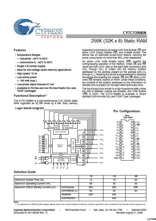
256K (32K x 8) Static RAMCY7C1399BNFeatures•Temperature Ranges —Industrial: –40°C to 85°C —Automotive-A: –40°C to 85°C •Single 3.3V power supply•Ideal for low-voltage cache memory applications •High speed: 12 ns •Low active power —180 mW (max.)•Low-power alpha immune 6T cell•Available in Pb-free and non Pb-free Plastic SOJ and TSOP I packagesFunctional Description [1]The CY7C1399BN is a high-performance 3.3V CMOS Static RAM organized as 32,768 words by 8 bits. Easy memoryexpansion is provided by an active LOW Chip Enable (CE) and active LOW Output Enable (OE) and tri-state drivers. The device has an automatic power-down feature, reducing the power consumption by more than 95% when deselected. An active LOW Write Enable signal (WE) controls the writing/reading operation of the memory. When CE and WE inputs are both LOW, data on the eight data input/output pins (I/O 0 through I/O 7) is written into the memory location addressed by the address present on the address pins (A 0through A 14). Reading the device is accomplished by selecting the device and enabling the outputs, CE and OE active LOW,while WE remains inactive or HIGH. Under these conditions,the contents of the location addressed by the information on address pins is present on the eight data input/output pins.The input/output pins remain in a high-impedance state unless the chip is selected, outputs are enabled, and Write Enable (WE) is HIGH. The CY7C1399BN is available in 28-pin standard 300-mil-wide SOJ and TSOP Type I packages.Note:1.For guidelines on SRAM system design, please refer to the ‘System Design Guidelines’ Cypress application note, available on the internet at .Selection Guide-12-15-20Maximum Access Time (ns)121520Maximum Operating Current (mA)555045Maximum CMOS Standby Current (µA)Commercial 500500500Commercial (L)505050Industrial 500500Automotive-A500Logic Block DiagramPin Configurations12345678910111415162019181721242322Top ViewSOJ 121325282726GNDA 6A 7A 8A 9A 10A 11A 12A 13WE V CC A 4A 3A 2A 1I/O 7I/O 6I/O 5I/O 4A 14A 5I/O 0I/O 1I/O 2CE OE A 0I/O 3A 1A 2A 3A 4A 5A 6A 7A 8COLUMN DECODERR O W D E C O D E RS E N S E A M P SINPUT BUFFERPOWER DOWNWE OEI/O 0CE I/O 1I/O 2I/O 332K x 8ARRAYI/O 7I/O 6I/O 5I/O 4A 9A 0A 11A 13A 12A 14A 10CY7C1399BNMaximum Ratings(Above which the useful life may be impaired. For user guide-lines, not tested.)Storage Temperature .................................–65°C to +150°C Ambient Temperature withPower Applied.............................................–55°C to +125°C Supply Voltage on V CC to Relative GND [2]....–0.5V to +4.6V DC Voltage Applied to Outputsin High Z State [2]....................................–0.5V to V CC + 0.5V DC Input Voltage [2].................................–0.5V to V CC + 0.5VOutput Current into Outputs (LOW).............................20 mA Static Discharge Voltage........................................... >2001V (per MIL-STD-883, Method 3015)Latch-Up Current.................................................... >200 mAPin Configuration2223242526272812510111514131216191817Top ViewTSOP 3420217689OE A 1A 2A 3A 4WE V CC A 5A 6A 7A 8A 9A 0CE I/O 7I/O 6I/O 5GND I/O 2I/O 1I/O 4I/O 0A 14A 10A 11A 13A 12I/O 3Operating RangeRange Ambient Temperature V CC Commercial 0°C to +70°C 3.3V ±300 mVIndustrial –40°C to +85°C Automotive-A–40°C to +85°CElectrical Characteristics Over the Operating Range [1]Parameter Description Test Conditions-12-15-20UnitMin.Max.Min.Max.Min.Max.V OH Output HIGH Voltage V CC = Min., I OH = –2.0 mA 2.4 2.42.4VV OL Output LOW Voltage V CC = Min., I OL = 4.0 mA0.40.40.4V V IH Input HIGH Voltage 2.2V CC + 0.3V 2.2V CC + 0.3V 2.2V CC + 0.3V V V IL Input LOW Voltage [2]–0.30.8–0.30.8–0.30.8V I IX Input Leakage Current –1+1–1+1–1+1µA I OZ Output Leakage Current GND ≤ V I ≤ V CC ,Output Disabled –5+5–5+5–5+5µA I CC V CC Operating Supply Current V CC = Max., I OUT = 0 mA, f = f MAX = 1/t RC 555045mA I SB1Automatic CE Power-Down Current— TTL Inputs Max. V CC , CE ≥ V IH , V IN ≥ V IH , or V IN ≤ V IL , f = f MAXComm’l 555mA Comm’l (L)44mAInd’l 55Auto-A5I SB2Automatic CE Power-Down Current— CMOS Inputs [3]Max. V CC , CE ≥ V CC – 0.3V , V IN ≥ V CC – 0.3V , or V IN ≤ 0.3V ,WE ≥V CC – 0.3V or WE ≤ 0.3V ,f =f MAXComm’l 500500500µA Comm’l (L)5050µA Ind’l 500500µA Auto-A500µANotes:2.Minimum voltage is equal to –2.0V for pulse durations of less than 20 ns.3.Device draws low standby current regardless of switching on the addresses.CY7C1399BNCapacitance [4]ParameterDescription Test ConditionsMax.Unit C IN : Addresses Input CapacitanceT A = 25°C, f = 1 MHz, V CC = 3.3V5pF C IN : Controls 6pF C OUTOutput Capacitance6pFAC Test Loads and Waveforms [5]Switching Characteristics Over the Operating Range [5]Parameter Description-12-15-20UnitMin.Max.Min.Max.Min.Max.Read Cycle t RC Read Cycle Time 121520ns t AA Address to Data Valid121520ns t OHA Data Hold from Address Change 333ns t ACE CE LOW to Data Valid 121520ns t DOE OE LOW to Data Valid 567ns t LZOE OE LOW to Low Z [6]0ns t HZOE OE HIGH to High Z [6, 7]566ns t LZCE CE LOW to Low Z [6]333ns t HZCE CE HIGH to High Z [6, 7]677ns t PU CE LOW to Power-Up 0ns t PD CE HIGH to Power-Down 121520ns Write Cycle [8, 9]t WC Write Cycle Time 121520ns t SCE CE LOW to Write End 81012ns t AW Address Set-Up to Write End 81012ns t HA Address Hold from Write End 000ns t SA Address Set-Up to Write Start 000ns t PWE WE Pulse Width81012ns t SD Data Set-Up to Write End 7810ns t HD Data Hold from Write End 0ns t HZWE WE LOW to High Z [8]777ns t LZWEWE HIGH to Low Z [6]333nsNotes:4.Tested initially and after any design or process changes that may affect these parameters.5.Test conditions assume signal transition time of 3 ns or less, timing reference levels of 1.5V, input pulse levels of 0 to 3.0V, and output loading of the specified I OL /I OH and capacitance C L = 30 pF.6.At any given temperature and voltage condition, t HZCE is less than t LZCE , t HZOE is less than t LZOE , and t HZWE is less than t LZWE for any given device.7.t HZOE , t HZCE , t HZWE are specified with C L = 5 pF as in AC Test Loads. Transition is measured ±500 mV from steady state voltage.8.The internal write time of the memory is defined by the overlap of CE LOW and WE LOW. Both signals must be LOW to initiate a write and either signal can terminate a write by going HIGH. The data input set-up and hold timing should be referenced to the rising edge of the signal that terminates the write.9.The minimum write cycle time for write cycle #3 (WE controlled, OE LOW) is the sum of t HZWE and t SD .3.0V 3.3V OUTPUT R1 317ΩR2351ΩC LINCLUDING JIG AND SCOPEGND90%10%90%10%≤3ns≤3nsOUTPUT1.73VEquivalent to:THÉVENIN E QUIVALENTALL INPUT PULSES 167ΩCY7C1399BNData Retention Characteristics (Over the Operating Range - L version only)Parameter DescriptionConditionsMin.Max.Unit V DR V CC for Data Retention 2.0V I CCDR Data Retention Current V CC = V DR = 2.0V,CE > V CC – 0.3V,V IN > V CC – 0.3V or V IN < 0.3V020µA t CDR Chip Deselect to Data Retention Time0ns t ROperation Recovery Timet RCnsData Retention Waveform3.0V 3.0V t CDRV DR >2VDATA RETENTION MODEt RCEV CC Switching WaveformsRead Cycle No. 1[10, 11]Read Cycle No. 2[11, 12]Notes:10.Device is continuously selected. OE, CE = V IL .11.WE is HIGH for read cycle.12.Address valid prior to or coincident with CE transition LOW.ADDRESSDATA OUTPREVIOUS DATA VALIDDATA VALIDt RCt AAt OHA50%50%DATA VALIDt RCt ACEt DOEt LZOEt LZCEt PUDATA OUTHIGH IMPEDANCEIMPEDANCEICCISBt HZOE t HZCEt PDOECEHIGH V CC SUPPLY CURRENTCY7C1399BNWrite Cycle No. 1 (WE Controlled)[8, 13, 14]Write Cycle No. 2 (CE Controlled)[8, 13, 14]Write Cycle No. 3 (WE Controlled, OE LOW)[9, 14]Notes:13.Data I/O is high impedance if OE = V IH .14.If CE goes HIGH simultaneously with WE HIGH, the output remains in a high-impedance state.15.During this period, the I/Os are in the output state and input signals should not be applied.Switching Waveforms (continued)t HDt SDt PWEt SAt HAt AWt WCDATA I/OADDRESSCEWEOEt HZOEDATA IN VALIDNOTE 15t WCt AWt SAt HAt HDt SDt SCEWEDATA I/OADDRESSCEDATA IN VALIDDATA I/OADDRESSt HDt SDt LZWEt SAt HAt AWt WCCEWEt HZWEDATA IN VALIDNOTE 15CY7C1399BN Truth TableCE WE OE Input/Output Mode PowerH X X High Z Deselect/Power-Down Standby (I SB)L H L Data Out Read Active (I CC)L L X Data In Write Active (I CC)L H H High Z Deselect, Output Disabled Active (I CC)Ordering InformationSpeed(ns)Ordering Code PackageDiagram Package TypeOperatingRange12CY7C1399BN-12VC51-8503128-Lead Molded SOJ Commercial CY7C1399BN-12VXC28-Lead Molded SOJ (Pb-free)CY7C1399BN-12ZC51-8507128-Lead TSOP ICY7C1399BN-12ZXC28-Lead TSOP I (Pb-free)CY7C1399BNL-12ZC28-Lead TSOP ICY7C1399BNL-12ZXC28-Lead TSOP I (Pb-free)CY7C1399BN-12VXI51-8503128-Lead Molded SOJ (Pb-free)Industrial 15CY7C1399BN-15VC28-Lead Molded SOJ Commercial CY7C1399BN-15VXC28-Lead Molded SOJ (Pb-free)CY7C1399BN-15ZC51-8507128-Lead TSOP ICY7C1399BN-15ZXC28-Lead TSOP I (Pb-free)CY7C1399BNL-15ZXC28-Lead TSOP I (Pb-free)CY7C1399BNL-15VXC51-8503128-Lead Molded SOJ (Pb-free)CY7C1399BN-15VI28-Lead Molded SOJ IndustrialCY7C1399BN-15VXI28-Lead Molded SOJ (Pb-free)CY7C1399BN-15ZI51-8507128-Lead TSOP ICY7C1399BN-15ZXI28-Lead TSOP I (Pb-free)CY7C1399BN-15VXA51-8503128-Lead Molded SOJ (Pb-free)Automotive-A 20CY7C1399BN-20ZXC51-8507128-Lead TSOP I (Pb-free)Commercial Please contact local sales representative regarding availability of these parts.CY7C1399BN Package DiagramsDocument #: 001-06490 Rev. *A Page 7 of 8CY7C1399BN Document History PageDocument Title: CY7C1399BN 256K (32K x 8) Static RAMDocument Number: 001-06490REV.ECN NO.ISSUEDATEORIG. OFCHANGE DESCRIPTION OF CHANGE**423877See ECN NXR New Data Sheet*A498575See ECN NXR Added Automotive-A rangeRemoved I OS parameter from DC Electrical Characteristics tableUpdated Ordering Information table.。