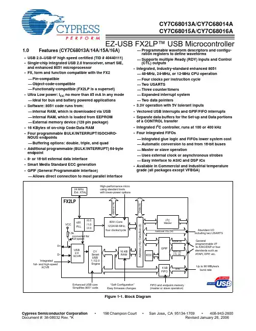
EZ-USB FX2LP™ USB MicrocontrollerCY7C68013A/CY7C68014A CY7C68015A/CY7C68016A1.0Features (CY7C68013A/14A/15A/16A)•USB 2.0–USB-IF high speed certified (TID # 40440111)•Single-chip integrated USB 2.0 transceiver, smart SIE, and enhanced 8051 microprocessor•Fit, form and function compatible with the FX2—Pin-compatible—Object-code-compatible—Functionally-compatible (FX2LP is a superset)•Ultra Low power: I CC no more than 85 mA in any mode —Ideal for bus and battery powered applications •Software: 8051 code runs from:—Internal RAM, which is downloaded via USB —Internal RAM, which is loaded from EEPROM —External memory device (128 pin package)•16 KBytes of on-chip Code/Data RAM•Four programmable BULK/INTERRUPT/ISOCHRO-NOUS endpoints—Buffering options: double, triple, and quad•Additional programmable (BULK/INTERRUPT) 64-byte endpoint•8- or 16-bit external data interface •Smart Media Standard ECC generation •GPIF (General Programmable Interface)—Allows direct connection to most parallel interface—Programmable waveform descriptors and configu-ration registers to define waveforms—Supports multiple Ready (RDY) inputs and Control (CTL) outputs•Integrated, industry-standard enhanced 8051—48-MHz, 24-MHz, or 12-MHz CPU operation —Four clocks per instruction cycle —Two USARTS—Three counter/timers—Expanded interrupt system —Two data pointers•3.3V operation with 5V tolerant inputs•Vectored USB interrupts and GPIF/FIFO interrupts •Separate data buffers for the Set-up and Data portions of a CONTROL transfer•Integrated I 2C controller, runs at 100 or 400 kHz •Four integrated FIFOs—Integrated glue logic and FIFOs lower system cost —Automatic conversion to and from 16-bit buses —Master or slave operation—Uses external clock or asynchronous strobes —Easy interface to ASIC and DSP ICs•Available in Commercial and Industrial temperature grade (all packages except VFBGA)A d d r e s s (16)x20PLL/0.5/1.0/2.08051 Core 12/24/48 MHz,four clocks/cycleI 2CVCC1.5kD+D–A d d r e s s (16) / D a t aB u s (8)FX2LPGPIFCY Smart USB 1.1/2.0EngineUSB 2.0XCVR16 KB RAM4 kB FIFOIntegrated full- and high-speedXCVRAdditional I/Os (24)ADDR (9)CTL (6)RDY (6)8/16D a t a (8)24 MHz Ext. XTALEnhanced USB core Simplifies 8051 code “Soft Configuration”Easy firmware changes FIFO and endpoint memory (master or slave operation)Up to 96 MBytes/s burst rateGeneralprogrammable I/F to ASIC/DSP or bus standards such as ATAPI, EPP , etc.Abundant I/Oincluding two USARTS High-performance micro using standard toolswith lower-power optionsMasterFigure 1-1. Block Diagramconnected for full speedECC1.1Features (CY7C68013A/14A only)•CY7C68014A: Ideal for battery powered applications —Suspend current: 100 µA (typ)•CY7C68013A: Ideal for non-battery powered applica-tions—Suspend current: 300 µA (typ)•Available in five lead-free packages with up to 40 GPIOs —128-pin TQFP (40 GPIOs), 100-pin TQFP (40 GPIOs),56-pin QFN (24 GPIOs), 56-pin SSOP (24 GPIOs), and 56-pin VFBGA (24 GPIOs)1.2Features (CY7C68015A/16A only)•CY7C68016A: Ideal for battery powered applications—Suspend current: 100 µA (typ)•CY7C68015A: Ideal for non-battery powered applica-tions—Suspend current: 300 µA (typ)•Available in lead-free 56-pin QFN package (26 GPIOs)—2 more GPIOs than CY7C68013A/14A enabling addi-tional features in same footprintCypress Semiconductor Corporation’s (Cypress’s) EZ-USB FX2LP™ (CY7C68013A/14A) is a low-power version of the EZ-USB FX2™ (CY7C68013), which is a highly integrated, low-power USB 2.0 microcontroller. By integrating the USB 2.0 transceiver, serial interface engine (SIE), enhanced 8051 microcontroller, and a programmable peripheral interface in a single chip, Cypress has created a very cost-effective solution that provides superior time-to-market advantages with low power to enable bus powered applications.The ingenious architecture of FX2LP results in data transfer rates of over 53 Mbytes per second, the maximum-allowable USB 2.0 bandwidth, while still using a low-cost 8051 microcon-troller in a package as small as a 56 VFBGA (5mm x 5mm). Because it incorporates the USB 2.0 transceiver, the FX2LP is more economical, providing a smaller footprint solution than USB 2.0 SIE or external transceiver implementations. With EZ-USB FX2LP, the Cypress Smart SIE handles most of the USB 1.1 and 2.0 protocol in hardware, freeing the embedded microcontroller for application-specific functions and decreasing development time to ensure USB compatibility. The General Programmable Interface (GPIF) and Master/Slave Endpoint FIFO (8- or 16-bit data bus) provides an easy and glueless interface to popular interfaces such as ATA, UTOPIA, EPP, PCMCIA, and most DSP/processors. The FX2LP draws considerably less current than the FX2 (CY7C68013), has double the on-chip code/data RAM and is fit, form and function compatible with the 56-, 100-, and 128-pin FX2.Five packages are defined for the family: 56VFBGA, 56 SSOP, 56 QFN, 100 TQFP, and 128 TQFP.2.0 Applications•Portable video recorder•MPEG/TV conversion•DSL modems•ATA interface•Memory card readers•Legacy conversion devices•Cameras•Scanners•Home PNA•Wireless LAN•MP3 players•NetworkingThe “Reference Designs” section of the Cypress web site provides additional tools for typical USB 2.0 applications. Each reference design comes complete with firmware source and object code, schematics, and documentation. Please visit for more information.3.0Functional Overview3.1USB Signaling SpeedFX2LP operates at two of the three rates defined in the USB Specification Revision 2.0, dated April 27, 2000:•Full speed, with a signaling bit rate of 12 Mbps •High speed, with a signaling bit rate of 480 Mbps.FX2LP does not support the low-speed signaling mode of 1.5Mbps.3.28051 MicroprocessorThe 8051 microprocessor embedded in the FX2LP family has 256 bytes of register RAM, an expanded interrupt system,three timer/counters, and two USARTs.3.2.18051 Clock FrequencyFX2LP has an on-chip oscillator circuit that uses an external 24-MHz (±100-ppm) crystal with the following characteristics:•Parallel resonant •Fundamental mode •500-µW drive level•12-pF (5% tolerance) load capacitors.An on-chip PLL multiplies the 24-MHz oscillator up to 480MHz, as required by the transceiver/PHY , and internal counters divide it down for use as the 8051 clock. The default 8051 clock frequency is 12 MHz. The clock frequency of the 8051 can be changed by the 8051 through the CPUCS register, dynamically.The CLKOUT pin, which can be three-stated and inverted using internal control bits, outputs the 50% duty cycle 8051clock, at the selected 8051 clock frequency—48, 24, or 12MHz.3.2.2USARTSFX2LP contains two standard 8051 USARTs, addressed via Special Function Register (SFR) bits. The USART interface pins are available on separate I/O pins, and are not multi-plexed with port pins.UART0 and UART1 can operate using an internal clock at 230KBaud with no more than 1% baud rate error. 230-KBaud operation is achieved by an internally derived clock source that generates overflow pulses at the appropriate time. The internal clock adjusts for the 8051 clock rate (48, 24, 12 MHz)such that it always presents the correct frequency for 230-KBaud operation.[1]3.2.3Special Function RegistersCertain 8051 SFR addresses are populated to provide fast access to critical FX2LP functions. These SFR additions are shown in Table 3-1. Bold type indicates non-standard,enhanced 8051 registers. The two SFR rows that end with “0”and “8” contain bit-addressable registers. The four I/O ports A–D use the SFR addresses used in the standard 8051 for ports 0–3, which are not implemented in FX2LP . Because of the faster and more efficient SFR addressing, the FX2LP I/O ports are not addressable in external RAM space (using the MOVX instruction).3.3I 2C BusFX2LP supports the I 2C bus as a master only at 100-/400-KHz.SCL and SDA pins have open-drain outputs and hysteresis inputs. These signals must be pulled up to 3.3V, even if no I 2C device is connected.3.4BusesAll packages: 8- or 16-bit “FIFO” bidirectional data bus, multi-plexed on I/O ports B and D. 128-pin package: adds 16-bit output-only 8051 address bus, 8-bit bidirectional data bus.Figure 3-1. Crystal Configuration12 pf12 pf24 MHz20 × PLLC1C212-pF capacitor values assumes a trace capacitanceof 3 pF per side on a four-layer FR4 PCANote:1.115-KBaud operation is also possible by programming the 8051 SMOD0 or SMOD1 bits to a “1” for UART0 and/or UART1, respectively.3.5USB Boot MethodsDuring the power-up sequence, internal logic checks the I2C port for the connection of an EEPROM whose first byte is either 0xC0 or 0xC2. If found, it uses the VID/PID/DID values in the EEPROM in place of the internally stored values (0xC0), or it boot-loads the EEPROM contents into internal RAM (0xC2). If no EEPROM is detected, FX2LP enumerates using internally stored descriptors. The default ID values for FX2LP are VID/PID/DID (0x04B4, 0x8613, 0xAxxx where xxx = Chip revision).[2]3.6ReNumeration™Because the FX2LP’s configuration is soft, one chip can take on the identities of multiple distinct USB devices.When first plugged into USB, the FX2LP enumerates automat-ically and downloads firmware and USB descriptor tables over the USB cable. Next, the FX2LP enumerates again, this time as a device defined by the downloaded information. This patented two-step process, called ReNumeration™, happens instantly when the device is plugged in, with no hint that the initial download step has occurred.Two control bits in the USBCS (USB Control and Status) register control the ReNumeration process: DISCON and RENUM. To simulate a USB disconnect, the firmware sets DISCON to 1. To reconnect, the firmware clears DISCON to 0. Before reconnecting, the firmware sets or clears the RENUM bit to indicate whether the firmware or the Default USB Device will handle device requests over endpoint zero: if RENUM = 0, the Default USB Device will handle device requests; if RENUM = 1, the firmware will.3.7Bus-powered ApplicationsThe FX2LP fully supports bus-powered designs by enumer-ating with less than 100 mA as required by the USB 2.0 speci-fication.3.8Interrupt System3.8.1INT2 Interrupt Request and Enable RegistersFX2LP implements an autovector feature for INT2 and INT4. There are 27 INT2 (USB) vectors, and 14 INT4 (FIFO/GPIF) vectors. See EZ-USB Technical Reference Manual (TRM) for more details.3.8.2USB-Interrupt AutovectorsThe main USB interrupt is shared by 27 interrupt sources. To save the code and processing time that normally would be required to identify the individual USB interrupt source, the FX2LP provides a second level of interrupt vectoring, called Autovectoring. When a USB interrupt is asserted, the FX2LP pushes the program counter onto its stack then jumps to address 0x0043, where it expects to find a “jump” instruction to the USB Interrupt service routine.Table 3-1. Special Function Registersx8x9x Ax Bx Cx Dx Ex Fx 0IOA IOB IOC IOD SCON1PSW ACC B 1SP EXIF INT2CLR IOE SBUF12DPL0MPAGE INT4CLR OEA3DPH0OEB4DPL1OEC5DPH1OED6DPS OEE7PCON8TCON SCON0IE IP T2CON EICON EIE EIP 9TMOD SBUF0A TL0AUTOPTRH1EP2468STAT EP01STAT RCAP2LB TL1AUTOPTRL1EP24FIFOFLGS GPIFTRIG RCAP2HC TH0reserved EP68FIFOFLGS TL2D TH1AUTOPTRH2GPIFSGLDATH TH2E CKCON AUTOPTRL2GPIFSGLDATLXF reserved AUTOPTRSET-UP GPIFSGLDATLNOXTable 3-2. Default ID Values for FX2LPDefault VID/PID/DIDVendor ID0x04B4Cypress SemiconductorProduct ID0x8613EZ-USB FX2LPDevice release0xAnnn Depends on chip revision(nnn = chip revision where firstsilicon = 001)Note:2.The I2C bus SCL and SDA pins must be pulled up, even if an EEPROM is not connected. Otherwise this detection method does not work properly.The FX2LP jump instruction is encoded as follows.If Autovectoring is enabled (AV2EN = 1 in the INTSET-UP register), the FX2LP substitutes its INT2VEC byte. Therefore, if the high byte (“page”) of a jump-table address is preloaded at location 0x0044, the automatically-inserted INT2VEC byte at 0x0045 will direct the jump to the correct address out of the 27 addresses within the page.3.8.3FIFO/GPIF Interrupt (INT4)Just as the USB Interrupt is shared among 27 individual USB-interrupt sources, the FIFO/GPIF interrupt is shared among 14 individual FIFO/GPIF sources. The FIFO/GPIF Interrupt, like the USB Interrupt, can employ autovectoring. Table3-4 shows the priority and INT4VEC values for the 14 FIFO/GPIF interrupt sources.Table 3-3. INT2 USB InterruptsUSB INTERRUPT TABLE FOR INT2 Priority INT2VEC Value Source Notes1 00SUDAV Set-up Data Available2 04 SOF Start of Frame (or microframe)3 08SUTOK Set-up Token Received4 0C SUSPEND USB Suspend request5 10USB RESET Bus reset6 14HISPEED Enteredhigh speed operation7 18 EP0ACK FX2LP ACK’d the CONTROL Handshake8 1C reserved9 20 EP0-IN EP0-IN ready to be loaded with data10 24 EP0-OUT EP0-OUT has USB data11 28 EP1-IN EP1-IN ready to be loaded with data12 2C EP1-OUT EP1-OUT has USB data13 30 EP2 IN: buffer available. OUT: buffer has data14 34 EP4 IN: buffer available. OUT: buffer has data15 38 EP6 IN: buffer available. OUT: buffer has data16 3C EP8 IN: buffer available. OUT: buffer has data17 40 IBN IN-Bulk-NAK (any IN endpoint)18 44reserved19 48 EP0PING EP0 OUT was Pinged and it NAK’d20 4C EP1PING EP1 OUT was Pinged and it NAK’d21 50 EP2PING EP2 OUT was Pinged and it NAK’d22 54 EP4PING EP4 OUT was Pinged and it NAK’d23 58 EP6PING EP6 OUT was Pinged and it NAK’d24 5C EP8PING EP8 OUT was Pinged and it NAK’d25 60 ERRLIMIT Bus errors exceeded the programmed limit26 6427 68 reserved28 6C reserved29 70 EP2ISOERR ISO EP2 OUT PID sequence error30 74 EP4ISOERR ISO EP4 OUT PID sequence error31 78 EP6ISOERR ISO EP6 OUT PID sequence error32 7C EP8ISOERR ISO EP8 OUT PID sequence errorIf Autovectoring is enabled (AV4EN = 1 in the INTSET-UP register), the FX 2LP substitutes its INT4VEC byte. Therefore, if the high byte (“page”) of a jump-table address is preloaded at location 0x0054, the automatically-inserted INT4VEC byte at 0x0055 will direct the jump to the correct address out of the 14 addresses within the page. When the ISR occurs, the FX2LP pushes the program counter onto its stack then jumps to address 0x0053, where it expects to find a “jump” instruction to the ISR Interrupt service routine.3.9Reset and Wakeup3.9.1Reset PinThe input pin, RESET#, will reset the FX2LP when asserted. This pin has hysteresis and is active LOW. When a crystal is used with the CY7C680xxA the reset period must allow for the stabilization of the crystal and the PLL. This reset period should be approximately 5 ms after VCC has reached 3.0V. If the crystal input pin is driven by a clock signal the internal PLL stabilizes in 200 µs after VCC has reached 3.0V[3]. Figure3-2 shows a power-on reset condition and a reset applied during operation. A power-on reset is defined as the time reset is asserted while power is being applied to the circuit. A powered reset is defined to be when the FX2LP has previously been powered on and operating and the RESET# pin is asserted. Cypress provides an application note which describes and recommends power on reset implementation and can be found on the Cypress web site. For more information on reset imple-mentation for the FX2 family of products visit the .Table 3-4. Individual FIFO/GPIF Interrupt SourcesPriority INT4VEC Value Source Notes 180EP2PF Endpoint 2 Programmable Flag2 84 EP4PF Endpoint 4 Programmable Flag388EP6PF Endpoint 6 Programmable Flag48C EP8PF Endpoint 8 Programmable Flag590EP2EF Endpoint 2 Empty Flag694EP4EF Endpoint 4 Empty Flag798EP6EF Endpoint 6 Empty Flag89C EP8EF Endpoint 8 Empty Flag9A0 EP2FF Endpoint 2 Full Flag10A4EP4FF Endpoint 4 Full Flag11 A8EP6FF Endpoint 6 Full Flag12AC EP8FF Endpoint 8 Full Flag13 B0GPIFDONE GPIF Operation Complete14 B4GPIFWF GPIF WaveformNote:3.If the external clock is powered at the same time as the CY7C680xxA and has a stabilization wait period, it must be added to the 200 µs.3.9.2Wakeup PinsThe 8051 puts itself and the rest of the chip into a power-down mode by setting PCON.0 = 1. This stops the oscillator and PLL. When WAKEUP is asserted by external logic, the oscil-lator restarts, after the PLL stabilizes, and then the 8051receives a wakeup interrupt. This applies whether or not FX2LP is connected to the USB.The FX2LP exits the power-down (USB suspend) state using one of the following methods:•USB bus activity (if D+/D– lines are left floating, noise on these lines may indicate activity to the FX2LP and initiate a wakeup).•External logic asserts the WAKEUP pin •External logic asserts the PA3/WU2 pin.The second wakeup pin, WU2, can also be configured as a general purpose I/O pin. This allows a simple external R-C network to be used as a periodic wakeup source. Note that WAKEUP is by default active LOW.3.10Program/Data RAM3.10.1SizeThe FX2LP has 16 KBytes of internal program/data RAM,where PSEN#/RD# signals are internally ORed to allow the 8051 to access it as both program and data memory. No USB control registers appear in this space.Two memory maps are shown in the following diagrams:Figure 3-3 Internal Code Memory, EA = 0Figure 3-4 External Code Memory, EA = 1.3.10.2Internal Code Memory, EA = 0This mode implements the internal 16-KByte block of RAM (starting at 0) as combined code and data memory. When external RAM or ROM is added, the external read and write strobes are suppressed for memory spaces that exist inside the chip. This allows the user to connect a 64-KByte memory without requiring address decodes to keep clear of internal memory spaces.Only the internal 16 KBytes and scratch pad 0.5 KBytes RAM spaces have the following access:•USB download •USB upload •Set-up data pointer •I 2C interface boot load.3.10.3External Code Memory, EA = 1The bottom 16 KBytes of program memory is external, and therefore the bottom 16 KBytes of internal RAM is accessible only as data memory.Figure 3-2. Reset Timing PlotsV IL 0V3.3V 3.0VT RESETVCCRESET#Power on ResetT RESETVCCRESET#V IL Powered Reset3.3V0VTable 3-5. Reset Timing ValuesConditionT RESET Power-on Reset with crystal 5 msPower-on Reset with external clock200 µs + Clock stability timePowered Reset 200 µsFigure 3-3. Internal Code Memory, EA = 0Inside FX2LPOutside FX2LP7.5 KBytes USB regs and 4K FIFO buffers (RD#,WR#)0.5 KBytes RAM Data (RD#,WR#)*(OK to populate data memory here—RD#/WR#strobes are not active)40 KBytes External Data Memory (RD#,WR#)(Ok to populate data memory here—RD#/WR#strobes are not active)16 KBytes RAM Code and Data(PSEN#,RD#,WR#)*48 KBytes External Code Memory (PSEN#)(OK to populate programmemory here—PSEN# strobe is not active)*SUDPTR, USB upload/download, I 2C interface boot accessFFFFE200E1FF E0003FFF0000DataCodeFigure 3-4. External Code Memory, EA = 1Inside FX2LPOutside FX2LP7.5 KBytes USB regs and 4K FIFO buffers (RD#,WR#)0.5 KBytes RAM Data (RD#,WR#)*(OK to populatedata memory here—RD#/WR#strobes are not active)40 KBytes External Data Memory (RD#,WR#)(Ok to populate data memory here—RD#/WR#strobes are not active)16 KBytes RAM Data(RD#,WR#)*64 KBytes External Code Memory (PSEN#)*SUDPTR, USB upload/download, I 2C interface boot accessFFFFE200E1FFE0003FFF0000DataCode3.11Register Addresses3.12Endpoint RAM3.12.1Size•3× 64 bytes (Endpoints 0 and 1)•8 × 512 bytes (Endpoints 2, 4, 6, 8)3.12.2Organization•EP0•Bidirectional endpoint zero, 64-byte buffer •EP1IN, EP1OUT•64-byte buffers, bulk or interrupt •EP2,4,6,8•Eight 512-byte buffers, bulk, interrupt, or isochronous. EP4 and EP8 can be double buffered, while EP2 and 6 can be either double, triple, or quad buffered. For high-speed end-point configuration options, see Figure 3-5.3.12.3Set-up Data BufferA separate 8-byte buffer at 0xE6B8-0xE6BF holds the Set-up data from a CONTROL transfer.3.12.4Endpoint Configurations (High-speed Mode)Endpoints 0 and 1 are the same for every configuration.Endpoint 0 is the only CONTROL endpoint, and endpoint 1 can be either BULK or INTERRUPT. The endpoint buffers can be configured in any 1 of the 12 configurations shown in the vertical columns. When operating in full-speed BULK mode only the first 64 bytes of each buffer are used. For example in high-speed, the max packet size is 512 bytes but in full-speed it is 64 bytes. Even though a buffer is configured to be a 512byte buffer, in full-speed only the first 64 bytes are used. The unused endpoint buffer space is not available for other opera-tions. An example endpoint configuration would be:FFFFE800E7BF E740E73F E700E6FF E500E4FF E480E47F E400E200E1FFE000E3FF EFFF2 KBytes RESERVED64 Bytes EP0 IN/OUT 64 Bytes RESERVED 8051 Addressable RegistersReserved (128)128 bytes GPIF Waveforms512 bytes 8051 xdata RAMF000(512)Reserved (512)E78064 Bytes EP1OUT E77F 64 Bytes EP1IN E7FF E7C0 4 KBytes EP2-EP8buffers(8 x 512)EP2–1024 double buffered; EP6–512 quad buffered (column 8).3.12.5Default Full-Speed Alternate Settings3.12.6Default High-Speed Alternate Settings6464645125121024102410241024102410241024512512512512512512512512512512EP0 IN&OUTEP1 IN EP1 OUTFigure 3-5. Endpoint Configuration1024102410245125125125125125125125125125125125125125125125125125125125125125125125125125125125125125121024102410241024102410245125121024102451251251251251251251251210241024512512512512512512646464646464646464646464646464646464646464646464646464646464646464123456789101112Table 3-6. Default Full-Speed Alternate Settings [4, 5]Alternate Setting 0123ep064646464ep1out 064 bulk 64 int 64 int ep1in 064 bulk 64 int 64 int ep2064 bulk out (2×)64 int out (2×)64 iso out (2×)ep4064 bulk out (2×)64 bulk out (2×)64 bulk out (2×)ep6064 bulk in (2×)64 int in (2×)64 iso in (2×)ep8064 bulk in (2×)64 bulk in (2×)64 bulk in (2×)Notes:4.“0” means “not implemented.”5.“2×” means “double buffered.”6.Even though these buffers are 64 bytes, they are reported as 512 for USB 2.0 compliance. The user must never transfer packets larger than 64 bytes to EP1.Table 3-7. Default High-Speed Alternate Settings [4, 5]Alternate Setting 0123ep064646464ep1out 0512 bulk [6]64 int 64 int ep1in 0512 bulk [6]64 int64 intep20512 bulk out (2×)512 int out (2×)512 iso out (2×)ep40512 bulk out (2×)512 bulk out (2×)512 bulk out (2×)ep60512 bulk in (2×)512 int in (2×)512 iso in (2×)ep80512 bulk in (2×)512 bulk in (2×)512 bulk in (2×)3.13External FIFO Interface3.13.1ArchitectureThe FX2LP slave FIFO architecture has eight 512-byte blocks in the endpoint RAM that directly serve as FIFO memories, and are controlled by FIFO control signals (such as IFCLK, SLCS#, SLRD, SLWR, SLOE, PKTEND, and flags).In operation, some of the eight RAM blocks fill or empty from the SIE, while the others are connected to the I/O transfer logic. The transfer logic takes two forms, the GPIF for internally generated control signals, or the slave FIFO interface for externally controlled transfers.3.13.2Master/Slave Control SignalsThe FX2LP endpoint FIFOS are implemented as eight physi-cally distinct 256x16 RAM blocks. The 8051/SIE can switch any of the RAM blocks between two domains, the USB (SIE) domain and the 8051-I/O Unit domain. This switching is done virtually instantaneously, giving essentially zero transfer time between “USB FIFOS” and “Slave FIFOS.” Since they are physically the same memory, no bytes are actually transferred between buffers.At any given time, some RAM blocks are filling/emptying with USB data under SIE control, while other RAM blocks are available to the 8051 and/or the I/O control unit. The RAM blocks operate as single-port in the USB domain, and dual-port in the 8051-I/O domain. The blocks can be configured as single, double, triple, or quad buffered as previ-ously shown.The I/O control unit implements either an internal-master (M for master) or external-master (S for Slave) interface.In Master (M) mode, the GPIF internally controls FIFOADR[1..0] to select a FIFO. The RDY pins (two in the 56-pin package, six in the 100-pin and 128-pin packages) can be used as flag inputs from an external FIFO or other logic if desired. The GPIF can be run from either an internally derived clock or externally supplied clock (IFCLK), at a rate that transfers data up to 96 Megabytes/s (48-MHz IFCLK with 16-bit interface).In Slave (S) mode, the FX2LP accepts either an internally derived clock or externally supplied clock (IFCLK, max. frequency 48 MHz) and SLCS#, SLRD, SLWR, SLOE, PKTEND signals from external logic. When using an external IFCLK, the external clock must be present before switching to the external clock with the IFCLKSRC bit. Each endpoint can individually be selected for byte or word operation by an internal configuration bit, and a Slave FIFO Output Enable signal SLOE enables data of the selected width. External logic must insure that the output enable signal is inactive when writing data to a slave FIFO. The slave interface can also operate asynchronously, where the SLRD and SLWR signals act directly as strobes, rather than a clock qualifier as in synchronous mode. The signals SLRD, SLWR, SLOE and PKTEND are gated by the signal SLCS#.3.13.3GPIF and FIFO Clock RatesAn 8051 register bit selects one of two frequencies for the internally supplied interface clock: 30 MHz and 48 MHz. Alter-natively, an externally supplied clock of 5 MHz–48 MHz feeding the IFCLK pin can be used as the interface clock. IFCLK can be configured to function as an output clock when the GPIF and FIFOs are internally clocked. An output enable bit in the IFCONFIG register turns this clock output off, if desired. Another bit within the IFCONFIG register will invert the IFCLK signal whether internally or externally sourced. 3.14GPIFThe GPIF is a flexible 8- or 16-bit parallel interface driven by a user-programmable finite state machine. It allows the CY7C68013A/15A to perform local bus mastering, and can implement a wide variety of protocols such as ATA interface, printer parallel port, and Utopia.The GPIF has six programmable control outputs (CTL), nine address outputs (GPIFADRx), and six general-purpose ready inputs (RDY). The data bus width can be 8 or 16 bits. Each GPIF vector defines the state of the control outputs, and deter-mines what state a ready input (or multiple inputs) must be before proceeding. The GPIF vector can be programmed to advance a FIFO to the next data value, advance an address, etc. A sequence of the GPIF vectors make up a single waveform that will be executed to perform the desired data move between the FX2LP and the external device.3.14.1Six Control OUT SignalsThe 100- and 128-pin packages bring out all six Control Output pins (CTL0-CTL5). The 8051 programs the GPIF unit to define the CTL waveforms. The 56-pin package brings out three of these signals, CTL0–CTL2. CTLx waveform edges can be programmed to make transitions as fast as once per clock (20.8 ns using a 48-MHz clock).3.14.2Six Ready IN SignalsThe 100- and 128-pin packages bring out all six Ready inputs (RDY0–RDY5). The 8051 programs the GPIF unit to test the RDY pins for GPIF branching. The 56-pin package brings out two of these signals, RDY0–1.3.14.3Nine GPIF Address OUT SignalsNine GPIF address lines are available in the 100- and 128-pin packages, GPIFADR[8..0]. The GPIF address lines allow indexing through up to a 512-byte block of RAM. If more address lines are needed, I/O port pins can be used.3.14.4Long Transfer ModeIn master mode, the 8051 appropriately sets GPIF transaction count registers (GPIFTCB3, GPIFTCB2, GPIFTCB1, or GPIFTCB0) for unattended transfers of up to 232 transactions. The GPIF automatically throttles data flow to prevent under or overflow until the full number of requested transactions complete. The GPIF decrements the value in these registers to represent the current status of the transaction.。