ISA(PC104)总线规范
- 格式:pdf
- 大小:993.05 KB
- 文档页数:19
PC104总线在某测试系统中的应用摘要:本文详细叙述了基于PC104总线在某测试系统中的应用,并详细介绍了该测试系统的硬件结构组成、工作原理,软件结构和测试流程。
关键词:PC104总线;测试系统;应用1引言PC104是一种专门为嵌入式控制而定义的工业控制总线,是一种优化的、小型的、堆栈式结构的嵌入式控制系统。
PC104与普通PC总线控制系统的主要不同点是:小尺寸结构:标准模块的机械尺寸是3.6英寸×3.8英寸,即90mm×96mm;堆栈式连接:去掉总线背板和插板滑道,总线模块之间总线的连接是通过上层的针和下层的孔相互咬合连接,这种层叠封装有极好的抗震性。
低功耗:减少元件数量和电源消耗,4mA总线驱动即可使模块正常工作,每个模块1W~2W能耗。
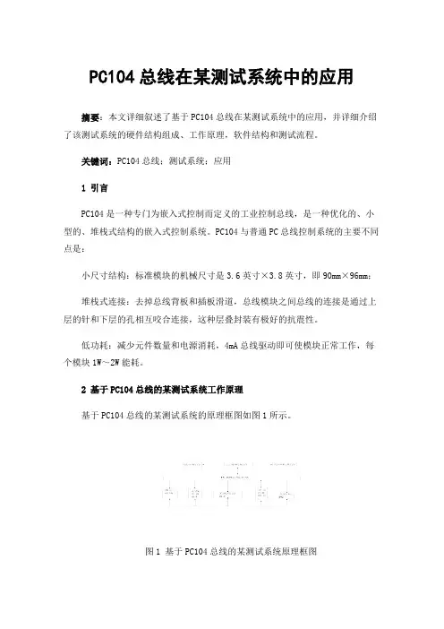
2基于PC104总线的某测试系统工作原理基于PC104总线的某测试系统的原理框图如图1所示。
图1 基于PC104总线的某测试系统原理框图在整个测试系统中,PC104总线系统由计算机进行控制,完成对被测系统所有信号的输出控制,所有需测量的数字量、模拟量的采集,检查及控制所有与被测系统的通信传输、激励仪器和测试仪器等。
被测系统主要由执行机构、无线电设备1、无线电设备2和动作机构组成。
该测试系统主要由A/D转换模块、D/A转换模块、I/O控制输入输出模块、通信系统和智能开关系统控制、激励仪器和测试仪器等组成。
PC104总线系统是测试系统完成自动配置的核心部件,它与计算机通过通信,接收计算机传来的数据并进行解析,将数据转化为控制指令按照时序完成数据采集、激励的施加、通信传输等,并将各个模块运行时的状态信息传回计算机,以保证计算机的管理软件可以实时控制信息处理组件的工作,在出现测试错误或状态不正常时及时关断电源,避免造成设备损坏。
另外各模块还可以在计算机的控制下完成状态复位,以保证各个模块当前状态不受原来测试配置的影响。
由于被测系统的参数种类数量繁多,各信号特性不尽相同,所以,需要专门设计信号匹配组合,将信号通过放大、滤波等操作,转换成为满足信息处理组合需要的、能够识别的标准信号。

HS-EIC100版本号V0.12008年11月28日广州市海山集成电路设计有限公司类别内容关键词HS-EIC100嵌入式工控主板,PC/104摘要讲解HS-EIC100产品上个接口说明及使用方法修订历史:版本编者日期描述V0.1 广州市海山集成电路设计有限公司2008/11/28 创建文档目录1.产品功能简介 (4)1.1产品概述 (4)1.2产品特性 (4)1.2.1硬件特性 (4)1.2.2软件特性 (5)1.3系统结构框图 (6)1.4产品应用 (6)1.5电气参数 (7)2.硬件结构说明 (7)2.1硬件结构布局 (7)2.2机械尺寸 (10)2.3资源列表 (10)2.3.1资源列表 (10)2.4接口说明及应用 (11)2.4.1电源输入接口 (11)2.4.2 PC/104总线接口 (12)2.4.3 系统复位接口 (16)2.4.4 JTAG调试接口 (16)2.4.5 RTC后备电池接口 (17)2.4.6 通讯接口 (17)2.4.7 PS2接口 (19)2.4.8 SD卡接口 (19)2.4.9 USB接口 (20)2.4.10 LCD接口 (20)2.4.11 VGA接口 (21)2.4.12 AC97接口 (23)2.4.13 通用数字IO接口 (24)3.声明 (24)4. 参考文献 (25)1.产品功能简介1.1产品概述HS-EIC100工控主板是广州市海山集成电路设计有限公司开发的基于本公司的32位处理器HS3210I处理器的可扩展的嵌入式工控主板,产品机械尺寸为PC/104外框尺寸(90mmX96mm),扩展总线为PC/104总线。
HS-EIC100工控主板具有资源丰富、接口齐全、可靠性高等特点。
具有以太网、CAN-BUS和LCD、I2C、UART、SPI、PS2、USB、RTC和AC97等丰富的外围接口。
可在-40℃~+80℃宽温度范围内稳定工作,满足工业级产品的各种应用需求。
PC/104-Plus SpecificationVersion1.2August2001Please NoteThis specification is subject to change without notice.While every effort has been made to ensure the accuracy of the material contained within this document,the PC/104Embedded Consortium shall under no circumstances be liable for incidental or consequential damages or related expenses resulting from the use of this specification.If errors are found,please notify the PC/104Embedded Consortium.PC/104and PC/104-Plus are trademarks of the PC/104Embedded Consortium.All other marks are the property of their respective companies.Copyright1992-2001,PC/104Embedded ConsortiumREVISION HISTORYDraft0.7,November20,1996-Preliminary Drafta.Formatted to meet the requirements of the PC/104Consortium.b.Modify the component restrictions across and to each side of the PC/104connectors(threesides,.400“from each edge,4.35"top clearance,.100"bottom clearance).Draft0.8,December16,1996-Cleanup for Releasea.Correct general typos.b.Correct word reference error.c.Add QuickSwitch part number and clarify Mux requirements.d.Change PCI ONLY to PCI-Only and add note.e.Correct figure4and Figure5errors.f.Correct typo in Table3.Draft0.9,January10,1997-Cleanup for Releasea.Cleanup minor grammatical errors.Version1.0,February1997-Initial Releasea.Grammatical changes and cleanup per review recommendations.b.Change Footnote1on Page2to show future support for the M66EN(66MHz Enable)signal.c.Add signals PRSNT[1:2]*and CLKRUN*to Figure1to encompass all unused PCI signals.d.Moved the Mechanical section after the Electrical section.e.Clarified the KEY pin usage for universal modules and defined them as ground connections.f.Clarified pin1for the PC/104-Plus connectors on Figure4.g.Added an example manufacturer and part No.for the PCI connector(Figure5)and Shroud(Figure6).h.Modified Figure2,Table1,and some text under Section2.2to add routing recommendationsfor the PCI interrupt lines INTA-INTD.Version1.1,June1997-Minor Editorial Correctionsa.Correct errors in the Table of Figures and Table of Tables.b.Correct dimensions on the PCI connector(Figure5).c.Correct part number and dimensions on the shroud(Figure6).d.Correct general typos and update reference information.Version1.2,April2001a.Added PCI Connector Specifications and PCI-104name for“PCI Only”.b.Added PC/1048-Bit and16-Bit Connector Specification.c.Removed specific company references.d.Corrected PCISIG and consortium addresses and phone numbers.TABLE OF CONTENTS1.INTRODUCTION (1)1.1S UMMARY OF K EY D IFFERENCES F ROM PC/104S PECIFICATION: (1)1.2S UMMARY OF K EY D IFFERENCES(120-PIN PCI AND PCI L OCAL B US S PECIFICATION) (1)1.3R EFERENCE S (1)2.PCI SIGNAL DEFINITION (2)2.1PCI B US S IGNAL D ESCRIPTION (3)2.1.1Address and Data (3)2.1.2Interface Control Pins (3)2.1.3Error Reporting (3)2.1.4Arbitration(Bus Masters Only) (3)2.1.5System (3)2.1.6Interrupts (3)2.2S IGNAL G ROUPING (4)3.ELECTRICAL SPECIFICATION (5)3.1PC/104B US (5)3.2PCI B US (5)3.2.1Signal Definitions (5)3.2.2Signal Assignments (5)3.2.3Power and Ground Pins (5)3.2.4Key Locations (5)3.2.5AC/DC Signal Specifications (5)3.3M ODULE P OWER R EQUIREMENTS (6)4.LEVELS OF CONFORMANCE (6)4.1PC/104-P LUS"C OMPLIANT" (6)4.2PC/104-P LUS"B US-COMPATIBLE" (6)4.3PCI-104 (6)5.MECHANICAL SPECIFICATION (7)5.1M ODULE D IMENSIONS (7)5.2C ONNECTOR AND S HROUD (7)6.TYPICAL MODULE STACK (8)APPENDICESA.MECHANICAL DIMENSIONS.........................................................................................A-1B.BUS SIGNAL ASSIGNMENTS..........................................................................................B-1TABLE OF FIGURESF IGURE1:PCI P IN L IST (2)F IGURE2:S IGNAL S ELECT (4)F IGURE3:T YPICAL M ODULE S TACK (8)F IGURE4:M ODULE D IMENSIONS..............................................................................................A-2 F IGURE5:PC/104-P LUS AND PCI-104PCI C ONNECTOR........................................................A-3 F IGURE6:PCI S HROUD.............................................................................................................A-3 F IGURE7:PC/104-P LUS AND PCI-104PCI C ONNECTOR S PECIFICATIONS............................A-4 F IGURE8:PC/1048-B IT AND16-B IT ISA C ONNECTOR S PECIFICATION................................A-5TABLE OF TABLEST ABLE1:R OTARY S WITCH S ETTINGS (4)T ABLE2:M ODULE P OWER R EQUIREMENTS (6)T ABLE3:PC/104-P LUS B US S IGNAL A SSIGNMENTS.................................................................B-2 T ABLE4:PC/104B US(R EFERENCE O NLY)..............................................................................B-3PC/104-Plus SPECIFICATIONVersion1.2August20011.INTRODUCTIONWhile the PC/AT architecture is becoming increasingly popular in embedded applications,there is an increasing need for a higher performance Bus throughput.This is especially true when it comes to graphics devices as well as other high speed I/O devices such as networks.This document supplies the mechanical and electrical specifications for the“PC/104-Plus”and incorporates all of the PC/104features,with the added advantage of the high speed PCI bus.The physical size,mounting configuration and electrical interconnect portion of the PC/104 specification shall remain unchanged.1.1Summary of Key Differences From PC/104Specification:! A third connector opposite the PC/104connectors supports the PCI bus.! Changes to the component height requirements increase the flexibility of the module.! Control logic added to handle the requirements for the high speed bus.1.2Summary of Key Differences(120-pin PCI and PCI Local Bus Specification)! The PCI bus connector is a4x30(120-pin)2mm pitch stackthrough connector as opposed to the124-pin edge connector on standard32-bit PCI Local Bus.! The120-pin PCI does not support64-bit Extensions,JTAG,PRSNT,or CLKRUN signals.1.3ReferencesThis document covers the addition of the PCI functions.The following documents should be used as reference for a detailed understanding of the overall system requirements:! PC/104Specification--Version2.4! PCI Local Bus Specification--Revision2.1Contact the PCI Special Interest Group office for the latest revision of the PCI specification:PCI Special Interest Group5440SW Westgate Drive,Suite217Portland,OR97221800.433.5177(U.S.)503.291.2569(International)If errors are found in this document,please send a written copy of the suggested corrections to:PC/104Embedded Consortium1060North Fourth St.San Jose,CA95112Tel650.903.8304Fax408.999.0344E-mail info@ Website 2.PCI SIGNAL DEFINITIONFigure 1shows the pins in functional groups,with the required pins on the left and the optional pins on the right side.The shaded pins on the right are unsupported features,but are included to show the entire PCI bus as defined in the PCI Revision 2.1Specification.This version of the PCI bus is intended as a 32-bit bus running at 33MHz and therefore,64-bit extension and 66MHz 1are not supported at this time.Also not supported are the boundary scan features (JTAG),Present (PRSNR[1:2]*),and Clock running (CLKRUN*).The direction indication on the pins assumes a combination master/target device.Figure 1:PCI Pin List1The PCI bus has been simulated at 33MHz.For the purpose of this specification,66MHz is not supported.Tosupport future enhancements,the M66EN signal should be grounded on any module that cannot support 66MHz and left open for modules that can support a 66MHz clock.(master Address &DataInterface ControlErrorReporting2.1PCI Bus Signal Description2.1.1Address and DataAD[31:00]Address and Data are multiplexed.A bus transaction consists of an addresscycle followed by one or more data cycles.C/BE[3:0]*Bus Command/Byte Enables are multiplexed.During the address cycle,thecommand is defined.During the Data cycle,they define the byte enables.PAR Parity is even on AD[31:00]and C/BE[3:0]*and is required.2.1.2Interface Control PinsFRAME*Frame is driven by the current master to indicate the start of a transaction andwill remain active until the final data cycle.TRDY*Target Ready indicates the selected devices ability to complete the currentdata cycle of the transaction.Both IRDY*and TRDY*must be asserted toterminate a data cycle.IRDY*Initiator Ready indicates the master's ability to complete the current datacycle of the transaction.STOP*Stop indicates the current selected device is requesting the master to stop thecurrent transaction.DEVSEL*Device Select is driven by the target device when its address is decoded.IDSEL Initialization Device Select is used as a chip-select during configuration.LOCK*Lock indicates an operation that may require multiple transactions tocomplete.2.1.3Error ReportingPERR*Parity Error is for reporting data parity errors.SERR*System Error is for reporting address parity errors.2.1.4Arbitration(Bus Masters Only)REQ*Request indicates to the arbitrator that this device desires use of the bus.GNT*Grant indicates to the requesting device that access has been granted.2.1.5SystemCLK Clock provides timing for all transactions on the PCI bus.RST*Reset is used to bring PCI-specific registers to a known state.2.1.6InterruptsINTA*Interrupt A is used to request Interrupts.INTB*Interrupt B is used to request Interrupts only for multi-function devices.INTC*Interrupt C is used to request Interrupts only for multi-function devices.INTD*Interrupt D is used to request Interrupts only for multi-function devices.2.2Signal GroupingA means of selecting the appropriate signals must be established that will easily allow for the installation and configuration of add-in PC/104-Plus modules.Figure 2shows such a method:Figure 2:Signal SelectThe multiplexer chips are Dual 4:1Mux/Demux chips.They provide a 5Ωswitch that connects the input and output together.These switches provide a bi-directional path with no signal propagation delay other than the RC delay of the on resistance of the switch and the load capacitance.This is typically 250ps at 50pF Load.Other methods of configuring the modules are possible,but the rotary switch is the most convenient,cleanest and provides for the least possible error in configuration.The clocks are tuned on the Host Board such that the length of CLK3trace is ≈0.662"less than CLK2,CLK2trace is ≈0.662"less than CLK1,and CLK1trace is ≈0.662"less than CLK0.Therefore,the first module on the stack must select CLK0(the longest trace),the second CLK1,etc.This provides basically no clock skew between modules.Table 1shows the appropriate switch setting and signals used for each module in the stack.It is recommended that additional Mux chips be added to route Interrupts if e one Mux for 1to 2Interrupts or two Mux's for 3to 4Interrupts.Table 1:Rotary Switch SettingsSwitch PositionModule SlotREQ*GNT*CLK ID Address INT0*INT1*INT2*INT3*0or 41REQ0*GNT0*CLK0AD20INTA*INTB*INTC*INTD*1or 52REQ1*GNT1*CLK1AD21INTB*INTC*INTD*INTA*2or 63REQ2*1GNT2*1CLK2AD22INTC*INTD*INTA*INTB*3or 74REQ2*1GNT2*1CLK3AD23INTD*INTA*INTB*INTC*Note 1:Because module slots 3and 4share REQ2/GNT2,they cannot both be bus master devices.3.ELECTRICAL SPECIFICATION3.1PC/104BusThe electrical specifications for the PC/104bus for bus drive current,bus termination,pullup/pulldown resistors,etc.are unchanged and are defined in the PC/104Specification.The signal assignments for the J1/P1and J2/P2connector are given in Appendix B,Table4:PC/104 Bus(Reference Only).3.2PCI BusThe PCI Bus mechanical interface is a stackable30x4header.This interface carries all of the required PCI signals per PCI Local Bus Specification Version.2.1.3.2.1Signal DefinitionsFor full details on the electrical requirements for the PCI bus,reference the PCI Local Bus Specification Version.2.1.3.2.2Signal AssignmentsSignals are assigned in the same relative order as in the PCI Local Bus Specification,but transformed to the corresponding header connector pins.Because of the stackthrough nature of the bus,slot-specific signals are duplicated for each plug-in module.The system has been designed to accommodate4PC/104-Plus modules,so multiple sets of the signals have been duplicated to accommodate one signal for each module.These four signal groups include: IDSEL[3:0]-CLK[3:0]-REQ*[2:0]-GNT*[2:0].Signal assignments for the J3/P3connector are given in Appendix B,Table3:PC/104-Plus Bus Signal Assignments.3.2.3Power and Ground PinsThe total number of power and ground signals remains the same,but the+3.3V pins have been reduced by two and the ground pins have been increased by two.The change was the result of signal grouping on the bus and has no effect on performance or integrity.3.2.4Key LocationsThe KEY pins are to guarantee proper module installation.Pin-A1will be removed and the female side plugged for5.0V I/O signals and Pin-D30will be modified in the same manner for3.3V I/O.Universal boards which can support either signal levels will have both key pins implemented.Universal boards must therefore be located at the top of the stack.See Appendix B,Table3:PC/104-Plus Bus Signal Assignments.3.2.5AC/DC Signal SpecificationsAll bus timing and signal levels are identical to the PCI Local Bus Specification Revision2.1.3.3Module Power RequirementsTable2specifies the voltage and maximum power requirements for each PC/104-Plus module. It should be noted that although the maximum requirements as specified are the same as the standard PC/104Specification,care should be used in designing PC/104-Plus modules to guarantee the least possible power consumption.A worst case module as specified could use almost39Watts of power,which would basically be unacceptable in most systems.Table2:Module Power RequirementsSupply Min.Voltage Max.Voltage Max.Current Max.Power+3.3V1 3.00 3.603A10.8W+5V 4.75 5.252A10.5W+12V11.412.61A12.6W-5V-5.25-4.750.2A 1.05W-12V-12.6-11.40.3A 3.78W Note1:Host Boards implementing“5volt PCI signaling”are not required to supply3.3volts to the modules, but must provide a bus and decoupling.If3.3volts is required for a module using the“5volt PCIsignaling”method,provisions should be made to provide its own3.3volts by means of an onboardregulator or some other input source.Host Boards implementing“3.3volt PCI signaling”arerequired to supply3.3volts to the modules.4.LEVELS OF CONFORMANCEThis section provides terminology intended to assist manufacturers and users of PC/104-Plus bus-compatible products in defining and specifying conformance with the PC/104-Plus Specification.4.1PC/104-Plus"Compliant"This refers to"PC/104-Plus form-factor"devices that conform to all non-optional aspects of the PC/104-Plus Specification,including both mechanical and electrical specifications.4.2PC/104-Plus"Bus-compatible"This refers to devices which are not"PC/104-Plus form-factor"(i.e.,do not comply with the module dimensions of the PC/104-Plus Specification),but provide male or female PC/104-Plus bus connectors that meets both the mechanical and electrical specifications provided for the PC/104-Plus bus connectors.4.3PCI-104Because the PC/104-Plus standard encompasses two different buses(i.e.PC/104104-pin"ISA" bus and120-pin"PCI"bus),it is possible for PC/104-Plus modules to implement only the PCI bus.Such modules shall have the designation"PCI-104".For example:PCI-104"Compliant" or PCI-104"Bus-compatible".This option precludes stacking standard PC/104Modules.5.MECHANICAL SPECIFICATION5.1Module DimensionsThe mechanical dimensions for this module are identical to PC/104Specification with the exception of the added connector(J3),some modifications to the I/O connector area,and changes to the component height restrictions.The component height on the top side has been reduced from0.435"to0.345"and the bottom has been increased from0.100"to0.190".The component restrictions across and to each side of the PC/104connectors(three sides,0.400"from each edge) remains the same as the PC/104Specification.The mechanical dimensions and restrictions are given in Appendix A,Figure4:Module Dimensions.5.2Connector and ShroudThe PC/104-Plus connector for the PCI bus is a4x30(120-pin)2mm pitch connector.The shroud should be installed on the bottom of the PC board when a stackthrough connector is used. The mechanical dimensions and restrictions are given in Appendix A,Figure5:PC/104-Plus and PCI-104PCI Connector.6.TYPICAL MODULE STACKFigure 3shows a typical module stack with 2PC/104-Plus modules,1PC/10416-Bit module,and 1PC/1048-Bit module.The maximum configuration for the PCI bus of PC/104-Plus modules is 4plus the Host Board.If standard PC/104modules are used in the stack,they must be the top module(s)because they will normally not include the PCI bus.Stackthrough8-bit moduleStackthrough16-bit moduleStackthroughPC/104-Plus moduleNon-stackthroughPC/104-Plus moduleAPPENDIX A MECHANICAL DIMENSIONSFigure4:Module Dimensions1Figure5:PC/104-Plus and PCI-104PCI ConnectorFigure6:PCI ShroudFigure7:PC/104-Plus and PCI-104PCI Connector Specifications MATERIALSHOUSING:HIGH TEMP THERMOPLASTIC,UL RATED94-V0 CONTACT:PHOSPHOR BRONZESOLDER:TIN-LEAD(63-37),IF APPLICABLESOLDER CLIP:ALUMINUM ALLOY,IF APPLICABLE CONTACT FINISHFEMALE INTERFACE:20MICROINCHES MINIMUM HARD GOLD MALE INTERFACE:GOLD FLASH MINIMUMSOLDER TAIL:100MICROINCHES MINIMUM SOLDER UNDERPLATE:50MICROINCHES MINIMUM NICKEL MECHANICAL PERFORMANCEINSERTION FORCE: 2.5OUNCE PER PIN MAXIMUMWITHDRAW FORCE:1OUNCE MINIMUM AVERAGENORMAL FORCE:50GRAMS MINIMUM(PER BEAM) DURABILITY:50CYCLES MINIMUMOPERATING TEMP:-55°C TO+85°CELECTRICAL PERFORMANCECONTACT RESISTANCE:<30MILLIOHMS MAXIMUMCURRENT CAPACITY:1AMP CONTINUOUS PER PINDIELECTRIC STRENGTH:500VACINSULATION RESISTANCE:5,000MEGOHMS MINIMUMFigure8:PC/1048-Bit and16-Bit ISA Connector SpecificationMATERIALSHOUSING:HIGH TEMP THERMOPLASTIC,UL RATED94-V0 CONTACT:PHOSPHOR BRONZESOLDER:TIN-LEAD(63-37),IF APPLICABLESOLDER CLIP:ALUMINUM ALLOY,IF APPLICABLE CONTACT FINISHFEMALE INTERFACE:20MICROINCHES MINIMUM HARD GOLD MALE INTERFACE:GOLD FLASH MINIMUMSOLDER TAIL:100MICROINCHES MINIMUM SOLDER UNDERPLATE:50MICROINCHES MINIMUM NICKEL MECHANICAL PERFORMANCEINSERTION FORCE: 3.5OUNCE PER PIN MAXIMUMWITHDRAW FORCE:1OUNCE MINIMUM AVERAGENORMAL FORCE:50GRAMS MINIMUM(PER BEAM) DURABILITY:50CYCLES MINIMUMOPERATING TEMP:-55°C TO+85°CELECTRICAL PERFORMANCECONTACT RESISTANCE:<30MILLIOHMS MAXIMUMCURRENT CAPACITY:1AMP CONTINUOUS PER PINDIELECTRIC STRENGTH:1000VACINSULATION RESISTANCE:5,000MEGOHMS MINIMUMAPPENDIX BBUS SIGNAL ASSIGNMENTSTable3:PC/104-Plus Bus Signal AssignmentsJ3/P3Pin A B C D1GND/5.0V KEY2Reserved+5AD002VI/O AD02AD01+5V3AD05GND AD04AD034C/BE0*AD07GND AD065GND AD09AD08GND6AD11VI/O AD10M66EN7AD14AD13GND AD128+3.3V C/BE1*AD15+3.3V9SERR*GND SB0*PAR10GND PERR*+3.3V SDONE11STOP*+3.3V LOCK*GND12+3.3V TRDY*GND DEVSEL*13FRAME*GND IRDY*+3.3V14GND AD16+3.3V C/BE2*15AD18+3.3V AD17GND16AD21AD20GND AD1917+3.3V AD23AD22+3.3V18IDSEL0GND IDSEL1IDSEL219AD24C/BE3*VI/O IDSEL320GND AD26AD25GND21AD29+5V AD28AD2722+5V AD30GND AD3123REQ0*GND REQ1*VI/O24GND REQ2*+5V GNT0*25GNT1*VI/O GNT2*GND26+5V CLK0GND CLK127CLK2+5V CLK3GND28GND INTD*+5V RST*29+12V INTA*INTB*INTC*30-12V Reserved Reserved GND/3.3V KEY2 Notes: 1.The shaded area denotes power or ground signals.2.The KEY pins are to guarantee proper module installation.Pin-A1will be removed and thefemale side plugged for5.0V I/O signals and Pin-D30will be modified in the same manner for3.3V I/O.It is recommended that both KEY pins(A1and D30)be electrically connected toGND for shielding.Table4:PC/104Bus(Reference Only)J1/P1Pin Row A Row B1IOCHCHK*GND2SD7RESETDRV3SD6+5V4SD5IRQ95SD4-5V6SD3DRQ2 J2/P27SD2-12V Pin Row D Row C8SD1ENDXFR* 0GND GND9SD0+12V1MEMCS16*SBHE*10IOCHRDY KEY2IOCS16*LA2311AEN SMEMW* 3IRQ10LA2212SA19SMEMR* 4IRQ11LA2113SA18IOW*5IRQ12LA2014SA17IOR*6IRQ15LA1915SA16DACK3* 7IRQ14LA1816SA15DRQ38DACK0*LA1717SA14DACK1* 9DRQ0MEMR*18SA13DRQ1 10DACK5*MEMW*19SA12REFRESH* 11DRQ5SD820SA11SYSCLK 12DACK6*SD921SA10IRQ713DRQ6SD1022SA9IRQ614DACK7*SD1123SA8IRQ515DRQ7SD1224SA7IRQ416+5V SD1325SA6IRQ317MASTER*SD1426SA5DACK2* 18GND SD1527SA4TC19GND KEY28SA3BALE29SA2+5V30SA1OSC31SA0GND32GND GND PC/104-Plus Specification Version1.2—Page B-3。
什么是PC/104PC/104(pc104)是一种嵌入式的总线规范。
提到PC/104,我们就必须提及著名的ISA总线,因为这二者之间有着天然的联系。
1981年,美国IBM公司制造出了世界上第一台个人计算机——PC机,与此同时,IBM 提出了PC总线(PC/XT总线),这是一种8位总线。
1984年,提出PC/AT总线,这是一种16位总线。
而为了开发与IBMPC兼容的外围设备,行业内便逐渐确立了以IBMPC总线规范为基础的ISA(工业标准架构:IndustryStandardArchitecture)总线。
1987年IEEE正式制订了ISA总线标准。
PC/104(pc104)是ISA(IEEE-996)标准的延伸。
1992年PC/104作为基本文件被采纳,叫做IEEE-P996.1兼容PC嵌入式模块标准。
PC/104是一种专门为嵌入式控制而定义的工业控制总线。
IEEE-P996是ISA工业总线规范,IEEE协会将它定义IEEE-P996.1,PC/104实质上就是一种紧凑型的IEEE-P996,其信号定义和PC/AT基本一致,但电气和机械规范却完全不同,是一种优化的、小型、堆栈式结构的嵌入式控制系统。
其小型化的尺寸(90x96mm),极低的功耗(典型模块为1-2瓦)和堆栈的总线形式(决定了其高可靠性),受到了众多从事嵌入式产品生产厂商的欢迎,在嵌入式系统领域逐渐流行开来。
截止目前,全世界已有200多家厂商在生产和销售符合PC/104规范的嵌入式板卡。
实际上,早在PC/104规范诞生之前,1987年就产生了世界上第一块PC/104板卡,由于其固有的优点,在国际上制订统一的规范之前,一直有许多厂商在生产类似的嵌入式板卡。
到了1992年,由业界著名的RTD公司和AM PRO公司等12家从事嵌入式系统开发的厂商发起,组建了国际PC/104协会,得到了全世界众多厂商纷纷响应,从此PC/104技术的发展走上了康庄大道。
ISA(PC104)总线规范ISA(PC/104) 总线信号时序简介SBS Science & Technology Co., Ltd.APPN-002ISA(PC/104)总线信号时序简介目录1.0 ISA概况2.0 ISA文献2.1 ISA规范 2.2 ISA书籍3.0 ISA结构形式4.0 PC/104结构形式5.0 ISA信号描述6.0 ISA 时序图7.0 ISA信号用法8.0 ISA连接器引脚9.0 PC/104总线连接引脚盛博科技1APPN-002ISA(PC/104)总线信号时序简介1.0 ISA 概况ISA总线即工业标准结构 Industry Standard Architecture 十世纪八十年代早期IBM在佛罗里达州Boca Raton研发实验室出的个人电脑其中包括了8位ISA总线 1984年最早起源于二 IBM于1981年推IBM推出了PC-AT 这是第一个全面实现16位结构的ISA总线IBM最初命名的AT总线首先被记录于IBM出版的 The PC-AT TechnicalReference 上此书包括了图表和BIOS清单这样类似于康柏的其它公司很容易就生产出了IBM兼容的产品由于IBM将AT总线”作为一项商标进行保护其它生产兼容IBM产品的公司就不能使用 AT总线这个名称结果人们在行业中创造了 ISA 并将其作为这种总线的新名称这个名称最后被包括IBM在内的所有公司采用尽管 The PC-AT Technical Reference 包含了详细的图表和BIOS清单但其因未包含严格的时序规范及其它必要条件而未成为一个很好的总线规范结果对ISA各种各样的实现造成了一些产品之间的兼容性问题的问题迄今为止渐渐形成了许多ISA总线规范但是不幸的是为了减轻因兼容造成这些规范也不尽相同没有产生出一个完全统一的ISA总线规范2.0 ISA 文献2.1 ISA 规范有关ISA总线规范的文档有如下几篇 EISA Specification, Version 3.12――这篇文档包括ISA总线规范并规定了扩展工业标准结构定义了ISA总线上32位扩展 IEEE Draft Standard P996 这篇文档描写了标准PC类系统的机械和电子规范通过/doc/4d9951778.html,/.付费可以向IEEE订购PS/2 Technical Reference 这篇来自IBM的文档内容包括在一些IBM 计算机PS/2线上使用ISA总线的信号定义和时序图2.2 ISA书籍两本对ISA总线进行了详细描述的书是 ISA & EISA Theory and Operation, by Edward Solari. (Annabooks) (ISBN 0-929392-15-9) ISA System Architecture, by Don Anderson and Tom Shanley. (MindShare) (ISBN 0-201-40996-8)盛博科技2APPN-002ISA(PC/104)总线信号时序简介3.0 ISA结构形式8 位卡:(At the card)(At the computer)16 位卡:(At the card)(At the computer)盛博科技3APPN-002ISA(PC/104)总线信号时序简介4.0 PC/104结构形式与ISA板不同义相同PC/104 8位/16位总线模块具有同样尺寸全为地 Gnd与ISA板总线信号定但多A32/B32;C0/D0;C19/D19引脚盛博科技4APPN-002ISA(PC/104)总线信号时序简介5.0 ISA 信号描述SA19-SA0System Address 地址位19:0用于对系统中内存和I/O设备的寻址内存寻址时使用SA19:SA0配合LA23:LA17 能寻址多达16兆的内存低16位,可以用来定位64K的I/O地址号在BALE为高时有效持有效 SA19是最高位 I/O寻址中只使用地址信SA0为最低位而由BALE的下降沿锁定通过读或写命令使信号保但也可以由ISA这些信号通常由系统微处理器或DMA控制器驱动扩展板的Bus Master 来取得ISA总线的控制权LA23-LA17Unlatched Address 23:17位是系统中内存地址址多达16兆的内存它们和SA19:SA0可以共同寻由于它们是非锁存的当BALE为高时这些信号才有效故在整个总线周期中它们并不总是保持有效状态用BALE下降沿锁存这些信号的译码AENAddress Enable 用于DMA传送过程中关闭总线系统微处理器和其它设备的传送通道制当AEN有效时总线上的地址数据和读写信号由DMA控制器控以防止DMA周期中出现不正确ISA扩展板的片选译码应包含AEN信号的片选BALEBuffered Address Latch Enable 用来锁存LA23:LA17信号或者译码这些信号 BALE下降沿用于锁存LA23:LA17 在DMA周期中BALE 被强制为高此信号与AEN并用时表明一个有效的微处理器或DMA地址CLKSystem Clock 是一个自行运转的时钟它的频率一般在7MHz到10MHz之间系统时钟在一些ISA板的应用中保证与该频率值在ISA 标准中并未严格定义系统微处理器的同步工作盛博科技5APPN-002ISA(PC/104)总线信号时序简介SD15 - SD0System Data SD15:SD0是ISA总线上的数据总线最低位 8位设备的数据传送通过SD7:SD0来完成其中SD15是最高位SD0是SD15:SD0则用于传送16位设备的数据当16位设备向8位设备传送数据时需将16位信号转换成两个8位周期通过SD7:SD0来进行传送-DACK0 to -DACK3 and -DACK5 to -DACK7DMA Acknowledge 0:3和5:7分别被用来确认DRQ0:DRQ3和DRQ5:DRQ7的 DMA请求DRQ0 to DRQ3 and DRQ5 to DRQ7DMA Requests 用于ISA板向DMA控制器提出服务请求或者Bus Master设备申请总线控制权的请求多个DMA请求可能同时断定有效发出请求的设备必须保持请求信号有效直到系统板发出相应的DACK信号-I/O CH CKI/O Channel Check I/O CH CK由ISA板生成进而引发非屏蔽中断时表明发现了不可恢复的错误当它有效I/O CH RDYI/O Channel Ready 允许较慢速ISA板通过插入等待状态延长I/O或内存读写周期好 I/O CH RDY通常处于高以插入等待状态就绪 ISA板将I/O CH RDY拉低未准备使用I/O CH RDY插入等待状态的设备需可以完成读写周期时地址译码和读/写信号有效后立即使I/O CH RDY信号为低当设备释放 I/O CH RDY回高-IORI/O Read 线上由总线控制设备驱动并且指令所选的I/O设备将数据读到数据总-IOWI/O Write 由总线控制设备驱动指令所选的I/O设备从数据总线上获取数据盛博科技6APPN-002ISA(PC/104)总线信号时序简介IRQ3 to IRQ7 and IRQ9 to IRQ12 and IRQ14 to IRQ15Interrupt Requests 向系统微处理器发出信号提示来自ISA板的请求当IRQ 线由低向高跳变时产生中断请求请求必须一直保持为高直到CPU通过其中断服务程序确认了这个请求请求有不同的优先权来自IRQ9:IRQ12 而来自IRQ3:IRQ 7IRQ14 :IRQ15的请求优先被处理的请求较后处理 IRQ7优先级最低IRQ9优先级最高-SMEMRSystem Memory Read 指令一个所选定的Memory设备将数据送到数据总线该信号仅在对1M以内的Memory空间读时才有效SMEMR来源于MEMR及低于1兆的存储译码-SMEMWSystem Memory Write 指令将当前数据总线上的数据写入一个所选定的 Memory设备该信号仅在对1M以内的Memory空间写时才有效 SMEMR来源于MEMR及低于1兆的存储译码-MEMRMemory Read 指令将一个所选定的Memory设备数据读出送到数据总线它在整个Memory存储读周期中都有效-MEMWMemory Write 指令将当前数据总线上的数据存储到一个所选定的Memory设备中它在整个Memory存储写周期中都有效-REFRESHMemory Refresh 该信号为低时表明正在进行内存刷新操作OSCOscillator 是一个时间段为70毫微秒的时钟(14.31818 MHz) 该信号与系统时钟不同步盛博科技7APPN-002ISA(PC/104)总线信号时序简介RESET DRVReset Drive在电源开启或系统复位时来复位或初始化系统逻辑高电平有效TCTerminal Count 在DMA通道操作中当计数完成时产生的终端计数信号-MASTERMaster 和DRQ线一起获得ISA板上ISA总线的控制权后权设备将MASTER信号拉低在此状态下使得其获得系统地址当接收到一个DACK 数据和控制线的控制在读/设备将在驱动地址和数据线之前等待一个时钟周期写命令之前等待两个时钟周期-MEM CS16Memory Chip Select 16 ISA板将该信号拉低以指示这是一个16位的Memory读写操作它由LA23:LA17地址线译码来驱动-I/O CS16I/O Chip Select 16 I/O设备将该信号拉低以指示这是一个16位的Memory读写操作它由SA15:SA0地址线译码来驱动-0WSZero Wait State 由一个总线从设备驱动使其拉低状态即可完成一个总线周期由地址译码产生说明不插入任何额外等待-OWS 完成一个无需等待的16位Memory周期-SBHESystem Byte High Enable 该信号为低时表明数据在数据总线高位部分传送(D15 至 D8)盛博科技8APPN-002ISA(PC/104)总线信号时序简介6.0 ISA总线时序图8位 I/O 总线周期BALE SA(15:0) -SBHE -IOR/W SD(7:0) (READ) SD(7:0) (WRITE) I/OCHRDY ________ __| |_________________________________________ _ ______________________________________________ __ _><______________________________________________><________________ _______ |______________________________| _____________ -------------------------------------<_____________>__________________________________ ----------------<__________________________________>__________________ _ _ _ _ _ _ _ _ _ _ _ _ _________ |________________________|8 位 Memory 总线循环_____ ________| |______________________________________ _ ________________ ________________________________ LA(23:17) _><________________><________________________________ _______ ________________________________________ __ SA(19:0) _______><________________________________________><________________ _______ -MEMR/W |______________________________| _____________ SD(7:0) -------------------------------------<_____________>(READ) __________________________________ SD(7:0) ----------------<__________________________________>(WRITE)__________________ _ _ _ _ _ _ _ _ _ _ _ _ _________ I/OCHRDY |________________________| BALE盛博科技9APPN-002ISA(PC/104)总线信号时序简介16 位 I/O 总线周期________ BALE SA(15:0) -IOCS16 -IOR/W SD(15:0) (READ) SD(15:0) (WRITE) I/OCHRDY ______________| |_____________________________ _____________ __________________________________ __ _____________><__________________________________><___________________ ___ |_______________________________| _____________________ ______ |________________________| __________________ -----------------------------<__________________>---________________________ -----------------------<________________________>---_______________________ _ _ _ _ _ _ _ _ _ _ ______ |___________________|16 位 Memory 总线周期BALE1 个或多个等待状态______ _________________| |____________________________ ___ ________________________ ______________________ LA(23:17) ___><________________________><______________________________________ ________________________________ _ SA(19:0) ________________><________________________________><_ _______ ______________________ -MEMCS16 |______________________| ________________________ ______ -MEMR/W |_____________________| _______________ SD(15:0) --------------------------------<_______________>---(READ) _____________________ SD(15:0) --------------------------<_____________________>---(WRITE)__________________________ _ _ _ _ _ _ _ _ __________ I/OCHRDY |_______________|盛博科技10APPN-002ISA(PC/104)总线信号时序简介6 位 Memory 总线周期BALE0 等待状态______ _________________| |____________________________ ___ ________________________ ______________________ LA(23:17) ___><________________________><______________________________________ _________________________ ________ SA(19:0) ________________><_________________________><________ _______ ______________________ -MEMCS16 |______________________| _________________________ ______________________ -0WS |____| ________________________ ________________ -MEMR/W |___________| ______ SD(15:0) --------------------------------<______>------------(READ) ____________ SD(15:0) --------------------------<____________>------------(WRITE)DMA 读DRQ(n) -DACK(n) AEN,BALE SA(15:0) -SBHE ______________ __| |___________________________________ _______________ __________ |__________________________| ____________________________________ ________| |_______ _______________ ___________________________ _______ _______________><___________________________><_______________________ ________________________ _________ SA(19:16) ________________><________________________><_________ LA(23:17) ____________________ __________ -MEMR |_____________________| ____________ SD(15:0) -------------------------------<____________>-------______________________ ___________ -IOW |__________________| __________ TC _______________________________| |__________ ________________________ _____________________ I/OCHRDY |______|盛博科技11APPN-002ISA(PC/104)总线信号时序简介DMA 写DRQ(n) -DACK(n) AEN,BALE SA(15:0) -SBHE ______________ __| |___________________________________ _______________ __________ |__________________________| ____________________________________ ________| |_______ _______________ ___________________________ _______ _______________><___________________________><_______________________ ________________________ _________ SA(19:16) ________________><________________________><_________ LA(23:17) ____________________ __________ -IOR |_____________________| ____________ SD(15:0) -------------------------------<____________>-------______________________ ___________ -MEMW |__________________| __________ TC _______________________________| |__________ ________________________ _____________________ I/OCHRDY |______| Bus Master 周期DRQ(n) -DACK(n) -MASTER AEN BALE SA(19:0) -SBHE ___________________________________ __| |______________ _______________ __________ |__________________________| __________________ _______ |__________________________| __________________ _______ ________| |__________________________| |_ _____________________________________________________ ________| |_ ________________________ ___________ ______________ ________________________><___________><_______________ ________________________ ___________ ______________ LA(23:17) ________________________><___________><___________________________________________ _________________ -IOR,-IOW |_____| -MEMR,-MEMW _____ SD(15:0) -------------------------------<_____>---------------盛博科技12APPN-002ISA(PC/104)总线信号时序简介内存刷新周期_______________ -REFRESH SA(9:0) -SMEMR I/OCHRDY _______________ |_____________________| _________________ ____________ _____________________________________><____________><__________________________________________ ________________ |_____________| _________________________ _ _ _ _ ___________________ |_______|7.0 ISA信号用法图例 I/O = 输入/输出 I = 输入 O = 输出 = 不需要的信号里表明这个信号是可选信号 I/O 出现在括号下表是 ISA 系统板上典型的信号使用情况Signal Name System Board Usage AEN BALE CLK -DACK DRQ -IO CS16 -I/O CH CK I/O CH RDY -IOR -IOW IRQ LA -MASTER O O O O I I I I/O I/O I/O I I/O ISignal Name -MEM CS16 -MEMR -MEMW OSC -REFRESH RESET DRV SA SD -SBHE -SMEMR -SMEMW TC -0WS System Board Usage I/O I/O I/O O I/O O I/O I/O I/O I/O I/O I/O I盛博科技13APPN-002ISA(PC/104)总线信号时序简介下表是 ISA 扩展板上典型的信号使用的情况Signal Name AEN BALE CLK -DACK DRQ -IO CS16 -I/O CH CK I/O CH DY -IOR -IOW IRQ LA(23:17) -MASTER -MEM CS16 -MEMR -MEMW OSC -REFRESH RESET DRV SA(16:0) SA(19:17) SD(7:0) SD(15:8) -SBHE -SMEMR -SMEMW TC -0WS ISA Bus Master (I) I O I (O) I O O (O) O O I O O (I) (O) I O I/O I/O O ISA 16-bit Mem Slave I (I) (O) (O) (O) I 0 I I (I) I I I (I) I/O I/O I (O) ISA 16-bit I/O Slave I (I) O (O) (O) I I (O) (I) I I I/O I/O I ISA 8-bit Mem Slave (I) (I) (O) (O) (O) (I) (I) (I) (I) I I I (I) I/O I I (O) ISA 8-bit I/O Slave I (I) (O) (O) I I (O) (I) I I I/O (O) ISA DMA Device (I) I O (O) I I (O) (I) I I/O (I/O) (I) -盛博科技14APPN-002ISA(PC/104)总线信号时序简介8.0 ISA 连接引脚Signal Name Pin Pin Signal Name Ground +5 V dc IRQ 9 -5 V dc DRQ2 -12 V dc -0WS +12 V dc Ground -SMEMW -SMEMR -IOW -IOR -DACK3 DRQ3 -DACK1 DRQ1 CLK IRQ7 IRQ6 IRQ5 IRQ4 IRQ3 -DACK2 TC BALE +5 V dc OSC Ground B1 A1 -I/O CH CK SD7 SD6 SD5 SD4 SD3 SD2 SD1 SD0 AEN SA19 SA18 SA17 SA16 SA15 SA14 SA13 SA12 SA11 SA10 SA9 SA8 SA7 SA6 SA5 SA4 SA3 SA2 SA1 SA0 B3 A3 B4 A4 B5 A5 B6 A6 B7 A7 B8 A8 B9 A9 B11 A11 B12 A12 B13 A13 B14 A14 B15 A15 B16 A16 B17 A17 B18 A18 B20 A20 B21 A21 B22 A22 B23 A23 B24 A24 B25 A25 B26 A26 B27 A27 B28 A28 B29 A29 B30 A30 B31 A31 Key RESET DRV B2 A2Signal Name Pin Pin Signal Name -MEM CS16 D1 C1 -IO CS16 IRQ10 IRQ11 IRQ12 IRQ15 IRQ14 -DACK0 DRQ0 -DACK5DRQ5 -DACK6 DRQ6 -DACK7 DRQ7 +5 V dc Ground D2 C2 D3 C3 D4 C4 D5 C5 D6 C6 D7 C7 D8 C8 D9 C9 D10 C10 D11 C11 D12 C12 D13 C13 D14 C14 D15 C15 D16 C16 D18 C18 -SBHE LA23 LA22 LA21 LA20 LA19 LA18 LA17 -MEMR -MEMW SD08 SD09 SD10 SD11 SD12 SD13 SD14 SD15B10 A10 I/O CH RDY-MASTER D17 C17-REFRESH B19 A19盛博科技15APPN-002ISA(PC/104)总线信号时序简介9.0 PC/104总线引脚引脚A1 A2 A3 A4 A5 A6 A7 A8 A9 A10 A11 A12 A13 A14 A15 A16 A17 A18 A19 A20 A21 A22 A23 A24 A25 A26 A27 A28 A29 A30 A31 A32信号名-IOCHCK SD7 SD6 SD5 SD4 SD3 SD2 SD1 SD0 IOCHRDY AEN SA19 SA18 SA17 SA16 SA15 SA14 SA13 SA12 SA11 SA10 SA9 SA8 SA7 SA6 SA5 SA4 SA3 SA2 SA1 SA0 GND用途Bus NMI input Data Bit 7 Data Bit 6 Data Bit 5 Data Bit 4 Data Bit 3 Data Bit 2 Data Bit 1 Data Bit 0 Processor Ready Ctrl Address Enable Address Bit 19 Address Bit 18 Address Bit 17 Address Bit 16 Address Bit 15 Address Bit 14 Address Bit 13 Address Bit 12 Address Bit 11 Address Bit 10 Address Bit 9 Address Bit 8 Address Bit 7 Address Bit 6 Address Bit 5 Address Bit 4 Address Bit 3 Address Bit 2 Address Bit 1 Address Bit 0 Ground P1AIn/OutIN I/O I/O I/O I/O I/O I/O I/O I/O IN I/O I/O I/O I/O I/O I/O I/O I/O I/O I/O I/O I/O I/O I/O I/O I/O I/O I/O I/O I/O I/O N/A PC/104 总线接口盛博科技16APPN-002ISA(PC/104)总线信号时序简介引脚B1 B2 B3 B4 B5 B6 B7 B8 B9 B10 B11 B12 B13 B14 B15 B16 B17 B18 B19 B20 B21 B22 B23 B24 B25 B26 B27 B28 B29 B30 B31 B32信号名GND RESET +5V IRQ9 -5V DRQ2 -12V ENDXFR +12V N/A -SMEMW -SMEMR -IOW -IOR -DACK3 DRQ3 -DACK1 DRQ1 -REFRESH SYSCLK IRQ7 IRQ6 IRQ5 IRQ4 IRQ3 -DACK2 T/C BALE +5V OSC GND GND用途Ground System Reset +5v Power Int Request 9 -5v Power DMA Request 2 -12v Power Zero wait state +12v Power Key Pin Mem Wrt, Io 1M Mem Rd, Io 1M I/O Write I/O read DMA Ack 3 DMA request 3 DMA Ack 1 DMA request 1 Memory Refresh Sys Clock Int Request 7 Int Request 6 Int Request 5 Int Request 4 Int Request 3 DMA Ack 2 Terminal Count Addrs Latch En +5v Power 14.3MHz Clk Ground Ground P1BIn/OutN/A OUT N/A IN N/A IN N/A IN N/A N/A I/O I/O I/O I/O OUT IN OUT IN I/O OUT IN IN IN IN IN OUT OUT OUT N/A OUT N/A N/APC/104 总线接口盛博科技17APPN-002ISA(PC/104)总线信号时序简介引脚C0 C1 C2 C3 C4 C5 C6 C7 C8 C9 C10 C11 C12 C13 C14 C15 C16 C17 C18 C19信号名GND SBHE LA23 LA22 LA21 LA20 LA19 LA18 LA17 -MEMR -MEMW SD8 SD9 SD10 SD11 SD12 SD13 SD14 SD15 Key 用途Ground Bus High Enable Address bit 23 Address bit 22 Address bit 21 Address bit 20 Address bit 19 Address bit 18 Address bit 17 Memory Read Memory Write Date Bit 8 Date Bit 9 Date Bit 10 Date Bit 11 Date Bit 12 Date Bit 13 Date Bit 14 Date Bit 15 Key Pin P2CIn/OutN/A I/O I/O I/O I/O I/O I/O I/O I/O I/O I/O I/O I/O I/O I/O I/O I/O I/O I/O N/APC/104 总线接口引脚D0 D1 D2 D3 D4 D5 D6 D7 D8 D9 D10 D11 D12 D13 D14 D15 D16 D17 D18 D19信号名GND -MEMCS16 -IOCS16 IRQ10 IRQ11 ** IRQ15 IRQ14 -DACK0 DRQ0 -DACK5 DRQ5 -DACK6 DRQ6 -DACK7 DRQ7 +5V -MASTER GND GND用途Ground 16-bit Mem Access 16-bit I/O Access Interrupt Request 10 Interrupt Request 11 Interrupt Request 15 Interrupt Request 14 DMA Acknowledge 0 DMA Request 0 DMA Acknowledge 5 DMA Request 5 DMA Acknowledge 6 DMA Request 6 DMA Acknowledge 7 DMA Request 7 +5V Power Bus Master Assert Ground Ground P2DIn/OutN/A IN IN IN IN IN IN OUT IN OUT IN OUT IN OUT IN N/A IN N/A N/APC/104 总线接口盛博科技18。
ISA总线ISA总线(或称工业标准结构总线)在与IBM兼容的PC系统刚起步时就已出现了(约1982年)。
实际上,任何早期PC中的功能卡均可插入最先进的基于Pentium4的计算机中,并且发挥作用。
这是因为在所有这些计算机都有ISA总线接口,从而与早期的PC仍然兼容。
ISA总线最近在家用计算机中已几乎不用了,但仍用于许多工业应用,且越来越受到限制。
ISA总线已经不同于它的早期版本。
ISA总线已从最初的8位标准总线发展为在大多数系统中广泛应用的16位标准总线。
在发展过程中甚至出现过一种称为EISA(扩展ISA)总线的32位标准总线,但已基本消失。
在一些比较老的主板上仍保留有ISA插槽,既可以插入8位ISA卡,又可以插入16位ISA卡。
32位的印制电路板则经常是PCI卡。
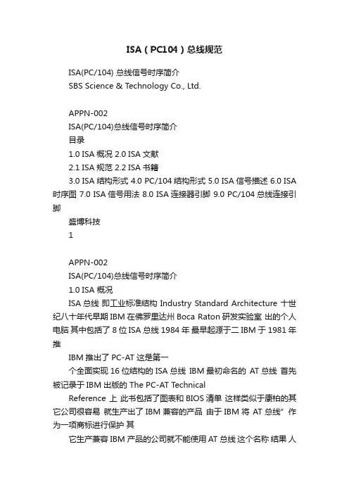
8位ISA总线接口引脚信号名称输入输出引脚信号名称输入输出A1I/OCHCK I B1GNDA2D7I/O B2RESET IA3D6I/O B3+5V IA4D5I/O B4IRQ2OA5D4I/O B5-5V IA6D3I/O B6DRQ2OA7D2I/O B7-12V IA8D1I/O B8NOWS OA9D0I/O B9+12V IA10IOCHRAY I/O B10GNDA11AEN I/O B11/SMEMW I/OA12A19I/O B12/SMEMR I/OA13A18I/O B13/IOW I/OA14A17I/O B14/IOR I/OA15A16I/O B15/DACK3IA16A15I/O B16DRQ3OA17A14I/O B17/DACK1IA18A13I/O B18DRQ1OA19A12I/O B19/REFRESH I/OA20A11I/O B20CLK IA21A10I/O B21IRQ7OA22A9I/O B22IRQ6OA23A8I/O B23IRQ5OA24A7I/O B24IRQ4OA25A6I/O B25IRQ3OA26A5I/O B26/DACK2IA27A4I/O B27T/C I/OA28A3I/O B28BALE IA29A2I/O B29+5V IA30A1I/O B30OSC IA31A0I/O B31GND1、下面对引脚信号做一些简要说明:D7~D0:8位数据线,双向,三态。
/AS-i总线技术及其应用0讲座第9讲AS-i总线的安装规范王俊杰0AS-i总线安装规范AS-i技术有3个显著的特点:第一是高度集成的AS-i专用集成电路芯片;第二是精确地检测差错代码的通信规则;第三是以智能/穿刺技术0为代表的AS-i总线安装规范。
AS-i机电一体化技术包括了AS-i电缆、绝缘穿刺技术、模块化结构以及各种AS-i元件等内容,它们对于实现开放式的互操作系统具有重要的意义。
1AS-i电缆1.1黄色标准电缆在AS-i系统中最简单的元件就是双线电缆。
它被用来向所连接的主站、从站和执行器、传感器传送数据和电源。
这种电缆是扁平的,因为只有这样才能精确地放置安装并使其适合于绝缘穿刺技术。
所以在系统连线时,完全不用剪断或拆除电缆或电缆芯的绝缘皮。
这种电缆的主要特征是:¹扁平形状的双线电缆;º外形尺寸约为8@4mm,电缆横截面为2@115mm2;»使用机械标准形状防止极性反接;¼非屏蔽;½经过特别精确绞合并符合VDE0295的6类标准的电缆结构;¾线芯颜色编码浅兰为(-),棕色为(+);¿可供选择的更灵活的大电流电缆(H05VV-F2@115符合DI N VDE0281)。
为确保不使极性接反,设计成扁条形式,只有在极性正确的情况下,电缆才能被放入设备中。
不规则的梯形横截面使元件的密封更加容易,如图1所示。
图1扁平电缆的横截面图电缆的横截面积为115mm2,在100m长的电缆上通以2A电流的情况下,在电缆末端的压降可以保持在3V以下,末端的执行器仍能够正常工作。
目前有几种标明了线缆外皮材料的电缆可供选择:¹EPR,橡胶混合物EM3,符合DIN VDE0207第21部分;ºTPE YM5,符合DIN VDE0207第5部分;»PUR,符合CENELEC HD22,T10。
第¹种电缆的电缆芯绝缘材料是由符合DI N VDE 0207第21部分的橡胶混合物3GI3所组成。
PC104总线PC/104总线是嵌入式PC机所用的总线标准.有两个总线插头.其中P1 有64个引脚, P2 有40个引脚共有104个引脚,这也是PC/104 名称的由来.PC104有两个版本,8位和16位,分别与PC和PC/AT相对应。
PC104PLUS 则与PCI总线相对应.PC/104模块本质上就是尺寸缩小为3.8英寸3.9英寸的ISA总线板卡。
它的总线与ISA 在IEEE-P996中定义基本相同。
具有16位数据宽度,最高工作频率为8MHz数据传输速率达到8MB/s,地址线24 条,可寻访16M字节地址单元。
所有PC/104总线信号定义和功能与它们在ISA总线相应部分是完全相同的。
104根线分为5类:地址线,数据线,控制线,时钟线,电源线。
简要介绍如下:(1)地址线SA0~SA19 和LA17~LA23SA0~SA19是可锁存的地址信号, LA17~LA23是非锁存信号由于没有锁存延迟因而给外设插板提供了一条快捷途径。
SA0~SA19加上LA17~LA23可实现16MB 空间寻址(其中SA17~SA19 和LA17~LA19 是重复的)(2)数据线数据线SD0~SD7 和SD8~SD15 其中SD0~SD7 位为低8位数据,SD8~SD15 为高8 位数据(3)控制线AEN:地址允许信号,输出线,高电平有效。
AEN=1,表明处于DMA控制周期;AEN=0,表示非DMA 周期。
此信号用来在DMA 期间禁止I/O端口的地址译码。
BALE:允许地址锁存,输出线。
这信号由总线控制器8288 提供,作为CPU 地址的有效标志。
当BALE 为高电平时将SA0~SA19 接到系统总线。
其下降沿用来锁存SA0~SA19IOR:I/O 读命令,输出线,低电平有效。
用来把选中的I/O设备的数据读到数据总线上,在CPU 启动的周期通过地址线选择I/O。
在DMA 周期,I/O设备由DACK选择IOW:I/O 写命令,输出线,低电平有效,用来把数据总线上的数据写入被选中的I/O 端口SMEMR和SMEMW:存储器读/写命令,低电平有效,用于对SA0~SA19 这20位地址寻址的1MB 内存的读/写操作MEMR和MEMW:低电平有效,存储器读/写命令,用于对24 位地址线全部存储空间读/写操作MEMCS16 和I/OCS16:它们是存储器16位片选信号和I/O16位片选信号,分别指明当前数据传送是16 位存储器周期和16 位I/O 周期SBHE:总线高字节允许信号,该信号有效时表示数据总线上传,送的是高位字节数据IRQ3~IRQ7 ,IRQ9 ,IRQ10~IRQ15 用于作为来自外部设备的中断请求输入线分别连在主片8259A 和从片8259A中断控制器的输入端。

ISA(PC/104) 总线信号时序简介SBS Science & Technology Co., Ltd.APPN-002ISA(PC/104)总线信号时序简介目录1.0 ISA概况 2.0 ISA文献2.1 ISA规范 2.2 ISA书籍3.0 ISA结构形式 4.0 PC/104结构形式 5.0 ISA信号描述 6.0 ISA时序图 7.0 ISA信号用法 8.0 ISA连接器引脚 9.0 PC/104总线连接引脚盛博科技1APPN-002ISA(PC/104)总线信号时序简介1.0 ISA 概况ISA总线 即工业标准结构 Industry Standard Architecture 十世纪八十年代早期IBM在佛罗里达州Boca Raton研发实验室 出的个人电脑 其中包括了8位ISA总线 1984年 最早起源于二 IBM于1981年推IBM推出了PC-AT 这是第一个全面实现16位结构的ISA总线 IBM最初命名的 AT总线 首先被记录于IBM出版的 The PC-AT TechnicalReference 上 此书包括了图表和BIOS清单 这样类似于康柏的其它公司很容易 就生产出了IBM兼容的产品 由于IBM将 AT总线”作为一项商标进行保护 其它生产兼容IBM产品的公司就不能使用 AT总线 这个名称 结果 人们在行业 中创造了 ISA 并将其作为这种总线的新名称 这个名称最后被包括IBM在内的所有公司采用 尽管 The PC-AT Technical Reference 包含了详细的图表和BIOS清单 但其 因未包含严格的时序 规范及其它必要条件而未成为一个很好的总线规范 结果 对ISA各种各样的实现造成了一些产品之间的兼容性问题 的问题 迄今为止 渐渐形成了许多ISA总线规范 但是不幸的是 为了减轻因兼容造成 这些规范也不尽相同没有产生出一个完全统一的ISA总线规范2.0 ISA 文献2.1 ISA 规范有关ISA总线规范的文档有如下几篇 EISA Specification, Version 3.12――这篇文档包括ISA总线规范 并规定了 扩展工业标准结构 定义了ISA总线上32位扩展 IEEE Draft Standard P996 这篇文档描写了标准PC类系统的机械和电 子规范 通过/.付费可以向IEEE订购 PS/2 Technical Reference 这篇来自IBM的文档内容包括在一些IBM计 算机PS/2线上使用ISA总线的信号定义和时序图2.2 ISA书籍两本对ISA总线进行了详细描述的书是 ISA & EISA Theory and Operation, by Edward Solari. (Annabooks) (ISBN 0-929392-15-9) ISA System Architecture, by Don Anderson and Tom Shanley. (MindShare) (ISBN 0-201-40996-8)盛博科技2APPN-002ISA(PC/104)总线信号时序简介3.0 ISA结构形式8 位卡:(At the card)(At the computer)16 位卡:(At the card)(At the computer)盛博科技3APPN-002ISA(PC/104)总线信号时序简介4.0 PC/104结构形式与ISA板不同 义相同PC/104 8位/16位总线模块具有同样尺寸 全为地 Gnd与ISA板总线信号定但多A32/B32;C0/D0;C19/D19引脚盛博科技4APPN-002ISA(PC/104)总线信号时序简介5.0 ISA 信号描述SA19-SA0System Address 地址位19:0用于对系统中内存和I/O设备的寻址 内存寻址时 使用SA19:SA0配合LA23:LA17 能寻址多达16兆的内存 低16位,可以用来定位64K的I/O地址 号在BALE为高时有效 持有效 SA19是最高位 I/O寻址中 只使用 地址信SA0为最低位而由BALE的下降沿锁定通过读或写命令使信号保 但也可以由ISA这些信号通常由系统微处理器或DMA控制器驱动扩展板的Bus Master 来取得ISA总线的控制权LA23-LA17Unlatched Address 23:17位是系统中内存地址 址多达16兆的内存 它们和SA19:SA0可以共同寻 由于它们是非锁存的 当BALE为高时这些信号才有效故在整个总线周期中它们并不总是保持有效状态 用BALE下降沿锁存这些信 号的译码AENAddress Enable 用于DMA传送过程中关闭总线系统微处理器和其它设备的 传送通道 制 当AEN有效时 总线上的地址 数据和读写信号由DMA控制器控 以防止DMA周期中出现不正确ISA扩展板的片选译码应包含AEN信号的片选BALEBuffered Address Latch Enable 用来锁存LA23:LA17信号或者译码这些信号 BALE下降沿用于锁存LA23:LA17 在DMA周期中BALE被强制为高 此信号 与AEN并用时表明一个有效的微处理器或DMA地址CLKSystem Clock 是一个自行运转的时钟 它的频率一般在7MHz到10MHz之间 系统时钟在一些ISA板的应用中保证与 该频率值在ISA标准中并未严格定义 系统微处理器的同步工作盛博科技5APPN-002ISA(PC/104)总线信号时序简介SD15 - SD0System Data SD15:SD0是ISA总线上的数据总线 最低位 8位设备的数据传送通过SD7:SD0来完成 其中SD15是最高位 SD0是 SD15:SD0则用于传送16位设备的数据 当16位设备向8位设备传送数据时 需将16位信号转换成两个8位 周期通过SD7:SD0来进行传送-DACK0 to -DACK3 and -DACK5 to -DACK7DMA Acknowledge 0:3和5:7分别被用来确认DRQ0:DRQ3和DRQ5:DRQ7的 DMA请求DRQ0 to DRQ3 and DRQ5 to DRQ7DMA Requests 用于ISA板向DMA控制器提出服务请求 或者Bus Master设备 申请总线控制权的请求 多个DMA请求可能同时断定有效 发出请求的设备必须保持请求信号有效直到系统板发出相应的DACK信号-I/O CH CKI/O Channel Check I/O CH CK由ISA板生成进而引发非屏蔽中断 时表明发现了不可恢复的错误 当它有效I/O CH RDYI/O Channel Ready 允许较慢速ISA板通过插入等待状态 延长I/O或内存读写 周期 好 I/O CH RDY通常处于高 以插入等待状态 就绪 ISA板将I/O CH RDY拉低 未准备使用I/O CH RDY插入等待状态的设备需可以完成读写周期时 地址译码和读/写信号有效后立即使I/O CH RDY信号为低 当设备释 放 I/O CH RDY回高-IORI/O Read 线上 由总线控制设备驱动 并且指令所选的I/O设备将数据读到数据总-IOWI/O Write 由总线控制设备驱动 指令所选的I/O设备从数据总线上获取数据盛博科技6APPN-002ISA(PC/104)总线信号时序简介IRQ3 to IRQ7 and IRQ9 to IRQ12 and IRQ14 to IRQ15Interrupt Requests 向系统微处理器发出信号 提示来自ISA板的请求 当IRQ 线由低向高跳变时产生中断请求 请求必须一直保持为高直到CPU通过其中断 服务程序确认了这个请求 请求有不同的优先权 来自IRQ9:IRQ12 而来自IRQ3:IRQ 7IRQ14 :IRQ15的请求优先被处理 的请求较后处理 IRQ7优先级最低IRQ9优先级最高-SMEMRSystem Memory Read 指令一个所选定的Memory设备将数据送到数据总线 该信号仅在对1M以内的Memory空间读时才有效 SMEMR来源于MEMR及低 于1兆的存储译码-SMEMWSystem Memory Write 指令将当前数据总线上的数据写入一个所选定的 Memory设备 该信号仅在对1M以内的Memory空间写时才有效 SMEMR来源 于MEMR及低于1兆的存储译码-MEMRMemory Read 指令将一个所选定的Memory设备数据读出送到数据总线 它在 整个Memory存储读周期中都有效-MEMWMemory Write 指令将当前数据总线上的数据存储到一个所选定的Memory设 备中 它在整个Memory存储写周期中都有效-REFRESHMemory Refresh 该信号为低时表明正在进行内存刷新操作OSCOscillator 是一个时间段为70毫微秒的时钟(14.31818 MHz) 该信号与系统时 钟不同步盛博科技7APPN-002ISA(PC/104)总线信号时序简介RESET DRVReset Drive在电源开启或系统复位时来复位或初始化系统逻辑 高电平有效TCTerminal Count 在DMA通道操作中当计数完成时产生的终端计数信号-MASTERMaster 和DRQ线一起获得ISA板上ISA总线的控制权 后 权 设备将MASTER信号拉低 在此状态下 使得其获得系统地址 当接收到一个DACK 数据和控制线的控制 在读/设备将在驱动地址和数据线之前等待一个时钟周期写命令之前等待两个时钟周期-MEM CS16Memory Chip Select 16 ISA板将该信号拉低以指示这是一个16位的Memory读 写操作 它由LA23:LA17地址线译码来驱动-I/O CS16I/O Chip Select 16 I/O设备将该信号拉低以指示这是一个16位的Memory读写操 作 它由SA15:SA0地址线译码来驱动-0WSZero Wait State 由一个总线从设备驱动使其拉低 状态即可完成一个总线周期 由地址译码产生 说明不插入任何额外等待 -OWS 完成一个无需等待的16位Memory周期-SBHESystem Byte High Enable 该信号为低时表明数据在数据总线高位部分传送(D15 至 D8)盛博科技8APPN-002ISA(PC/104)总线信号时序简介6.0 ISA总线时序图8位 I/O 总线周期BALE SA(15:0) -SBHE -IOR/W SD(7:0) (READ) SD(7:0) (WRITE) I/OCHRDY ________ __| |_________________________________________ _ ______________________________________________ __ _><______________________________________________><__ ______________ _______ |______________________________| _____________ -------------------------------------<_____________>__________________________________ ----------------<__________________________________>__________________ _ _ _ _ _ _ _ _ _ _ _ _ _________ |________________________|8 位 Memory 总线循环_____ ________| |______________________________________ _ ________________ ________________________________ LA(23:17) _><________________><________________________________ _______ ________________________________________ __ SA(19:0) _______><________________________________________><__ ______________ _______ -MEMR/W |______________________________| _____________ SD(7:0) -------------------------------------<_____________>(READ) __________________________________ SD(7:0) ----------------<__________________________________>(WRITE) __________________ _ _ _ _ _ _ _ _ _ _ _ _ _________ I/OCHRDY |________________________| BALE盛博科技916位I/O总线周期________BALE ______________| |_____________________________ _____________ __________________________________ __ SA(15:0) _____________><__________________________________><__ _________________ ___ -IOCS16 |_______________________________|_____________________ ______ -IOR/W |________________________|__________________SD(15:0) -----------------------------<__________________>---- (READ)________________________SD(15:0) -----------------------<________________________>---- (WRITE)_______________________ _ _ _ _ _ _ _ _ _ _ ______I/OCHRDY |___________________|16位Memory总线周期1个或多个等待状态______BALE _________________| |____________________________ ___ ________________________ ______________________ LA(23:17) ___><________________________><______________________ ________________ ________________________________ _ SA(19:0) ________________><________________________________><_ _______ ______________________ -MEMCS16 |______________________|________________________ ______ -MEMR/W |_____________________|_______________SD(15:0) --------------------------------<_______________>---- (READ)_____________________SD(15:0) --------------------------<_____________________>---- (WRITE)__________________________ _ _ _ _ _ _ _ _ __________ I/OCHRDY |_______________|6位Memory总线周期0等待状态______BALE _________________| |____________________________ ___ ________________________ ______________________ LA(23:17) ___><________________________><______________________ ________________ _________________________ ________ SA(19:0) ________________><_________________________><________ _______ ______________________ -MEMCS16 |______________________|_________________________ ______________________ -0WS |____|________________________ ________________ -MEMR/W |___________|______SD(15:0) --------------------------------<______>------------- (READ)____________SD(15:0) --------------------------<____________>------------- (WRITE)DMA读______________DRQ(n) __| |___________________________________ _______________ __________ -DACK(n) |__________________________|____________________________________AEN,BALE ________| |_______ _______________ ___________________________ _______ SA(15:0) _______________><___________________________><_______ -SBHE________________ ________________________ _________ SA(19:16) ________________><________________________><_________ LA(23:17)____________________ __________ -MEMR |_____________________|____________SD(15:0) -------------------------------<____________>-------- ______________________ ___________ -IOW |__________________|__________TC _______________________________| |__________ ________________________ _____________________ I/OCHRDY |______|DMA写______________DRQ(n) __| |___________________________________ _______________ __________ -DACK(n) |__________________________|____________________________________AEN,BALE ________| |_______ _______________ ___________________________ _______ SA(15:0) _______________><___________________________><_______ -SBHE________________ ________________________ _________ SA(19:16) ________________><________________________><_________ LA(23:17)____________________ __________ -IOR |_____________________|____________SD(15:0) -------------------------------<____________>-------- ______________________ ___________ -MEMW |__________________|__________TC _______________________________| |__________ ________________________ _____________________ I/OCHRDY |______|Bus Master周期___________________________________DRQ(n) __| |______________ _______________ __________ -DACK(n) |__________________________|__________________ _______ -MASTER |__________________________|__________________ _______ AEN ________| |__________________________| |_ _____________________________________________________ BALE ________| |_ ________________________ ___________ ______________ SA(19:0) ________________________><___________><_______________ -SBHE________________________ ___________ ______________ LA(23:17) ________________________><___________><___________________________________________ _________________ -IOR,-IOW |_____|-MEMR,-MEMW_____SD(15:0) -------------------------------<_____>---------------内存刷新周期_______________ _______________ -REFRESH |_____________________|_________________ ____________ ____________________ SA(9:0) _________________><____________><____________________ ______________________ ________________ -SMEMR |_____________|_________________________ _ _ _ _ ___________________ I/OCHRDY |_______|7.0 ISA信号用法图例I/O = 输入/输出I = 输入O = 输出- = 不需要的信号I/O出现在括号里表明这个信号是可选信号下表是ISA系统板上典型的信号使用情况Signal Name System Board Usage Signal Name System BoardUsageAEN O-MEM CS16 I/O BALE O-MEMR I/O CLK O-MEMW I/O -DACK O OSC O DRQ I-REFRESH I/O -IO CS16 I RESET DRV O -I/O CH CK I SA I/O I/O CH RDY I/O SD I/O -IOR I/O-SBHE I/O -IOW I/O-SMEMR I/O IRQ I-SMEMW I/O LA I/O TC I/O -MASTER I-0WS I下表是ISA扩展板上典型的信号使用的情况Signal Name ISA BusMasterISA 16-bitMem SlaveISA 16-bitI/O SlaveISA 8-bitMem SlaveISA 8-bitI/O SlaveISA DMADeviceAEN --I-I-BALE -I-(I)--CLK (I)(I)(I)(I)(I)(I) -DACK I----I DRQ O----O -IO CS16 I-O----I/O CH CK(O)(O)(O)(O)(O)(O) I/O CH DY I(O)(O)(O)(O)--IOR O-I-I I -IOW O-I-I I IRQ (O)(O)(O)(O)(O)(O) LA(23:17) O I-(I)---MASTER O------MEM CS16 I0-----MEMR O I-(I)---MEMW O I-(I)--OSC (I)(I)(I)(I)(I)(I) -REFRESH (O)I-I--RESET DRV I I I I I I SA(16:0) O I I I I-SA(19:17) -(I)-(I)--SD(7:0) I/O I/O I/O I/O I/O I/O SD(15:8) I/O I/O I/O--(I/O) -SBHE O I I----SMEMR ---I---SMEMW ---I--TC -----(I) -0WS -(O)-(O)(O)-8.0 ISA 连接引脚Signal Name Pin Pin Signal Name Ground B1A1-I/O CH CK RESET DRV B2A2SD7+5 V dc B3A3SD6IRQ 9B4A4SD5-5 V dc B5A5SD4DRQ2B6A6SD3-12 V dc B7A7SD2-0WS B8A8SD1+12 V dc B9A9SD0Ground B10A10I/O CH RDY -SMEMW B11A11AEN-SMEMR B12A12SA19-IOW B13A13SA18-IOR B14A14SA17-DACK3B15A15SA16DRQ3B16A16SA15-DACK1B17A17SA14DRQ1B18A18SA13-REFRESH B19A19SA12 CLK B20A20SA11IRQ7B21A21SA10IRQ6B22A22SA9IRQ5B23A23SA8IRQ4B24A24SA7IRQ3B25A25SA6-DACK2B26A26SA5TC B27A27SA4BALE B28A28SA3+5 V dc B29A29SA2OSC B30A30SA1Ground B31A31SA0Key Signal Name Pin Pin Signal Name -MEM CS16D1C1-SBHE-IO CS16D2C2LA23IRQ10D3C3LA22IRQ11D4C4LA21IRQ12D5C5LA20IRQ15D6C6LA19IRQ14D7C7LA18-DACK0D8C8LA17DRQ0D9C9-MEMR -DACK5D10C10-MEMWDRQ5D11C11SD08-DACK6D12C12SD09DRQ6D13C13SD10-DACK7D14C14SD11DRQ7D15C15SD12+5 V dc D16C16SD13-MASTER D17C17SD14Ground D18C18SD159.0 PC/104总线引脚引脚信号名用途In/OutA1 -IOCHCK Bus NMI input INA2 SD7 Data Bit 7 I/OA3 SD6 Data Bit 6 I/OA4 SD5 Data Bit 5 I/OA5 SD4 Data Bit 4 I/OA6 SD3 Data Bit 3 I/OA7 SD2 Data Bit 2 I/OA8 SD1 Data Bit 1 I/OA9 SD0 Data Bit 0 I/OA10 IOCHRDY Processor Ready Ctrl INEnable I/O A11 AEN AddressA12 SA19 Address Bit 19 I/OA13 SA18 Address Bit 18 I/OA14 SA17 Address Bit 17 I/OA15 SA16 Address Bit 16 I/OA16 SA15 Address Bit 15 I/OA17 SA14 Address Bit 14 I/OA18 SA13 Address Bit 13 I/OA19 SA12 Address Bit 12 I/OA20 SA11 Address Bit 11 I/OA21 SA10 Address Bit 10 I/OA22 SA9 Address Bit 9 I/OA23 SA8 Address Bit 8 I/OA24 SA7 Address Bit 7 I/OA25 SA6 Address Bit 6 I/OA26 SA5 Address Bit 5 I/OA27 SA4 Address Bit 4 I/OA28 SA3 Address Bit 3 I/OA29 SA2 Address Bit 2 I/OA30 SA1 Address Bit 1 I/OA31 SA0 Address Bit 0 I/OA32 GND Ground N/APC/104总线接口P1A引脚信号名用途In/OutB1 GND Ground N/AReset OUT B2 RESET SystemPower N/A B3 +5V +5vB4 IRQ9 Int Request 9 INPower N/A B5 -5V -5vB6 DRQ2 DMA Request 2 INPower N/A B7 -12V -12vB8 ENDXFR Zero wait state INPower N/A B9 +12V +12vPin N/A B10 N/A KeyB11 -SMEMW Mem Wrt, Io 1M I/OB12 -SMEMR Mem Rd, Io 1M I/OWrite I/O B13 -IOW I/Oread I/O B14 -IOR I/OB15 -DACK3 DMA Ack 3 OUTB16 DRQ3 DMA request 3 INB17 -DACK1 DMA Ack 1 OUTB18 DRQ1 DMA request 1 INB19 -REFRESH MemoryRefresh I/OClock OUTB20 SYSCLK SysB21 IRQ7 Int Request 7 INB22 IRQ6 Int Request 6 INB23 IRQ5 Int Request 5 INB24 IRQ4 Int Request 4 INB25 IRQ3 Int Request 3 INB26 -DACK2 DMA Ack 2 OUTCount OUT B27 T/C TerminalB28 BALE Addrs Latch En OUTPower N/A B29 +5V +5vClk OUT B30 OSC 14.3MHzB31 GND Ground N/A B32 GND Ground N/APC/104总线接口P1B引脚信号名用途In/OutC0 GND Ground N/A C1 SBHE Bus High Enable I/OC2 LA23 Address bit 23 I/OC3 LA22 Address bit 22 I/OC4 LA21 Address bit 21 I/OC5 LA20 Address bit 20 I/OC6 LA19 Address bit 19 I/OC7 LA18 Address bit 18 I/OC8 LA17 Address bit 17 I/ORead I/O C9 -MEMR MemoryWrite I/OC10 -MEMW MemoryC11 SD8 Date Bit 8 I/OC12 SD9 Date Bit 9 I/OC13 SD10 Date Bit 10 I/OC14 SD11 Date Bit 11 I/OC15 SD12 Date Bit 12 I/OC16 SD13 Date Bit 13 I/OC17 SD14 Date Bit 14 I/OC18 SD15 Date Bit 15 I/OPin N/AC19 Key KeyPC/104总线接口P2C引脚信号名用途In/OutD0 GND Ground N/A D1 -MEMCS16 16-bit Mem Access IND2 -IOCS16 16-bit I/O Access IND3 IRQ10 Interrupt Request 10 IND4 IRQ11 Interrupt Request 11 IND5 **D6 IRQ15 Interrupt Request 15 IND7 IRQ14 Interrupt Request 14 IND8 -DACK0 DMA Acknowledge 0 OUTD9 DRQ0 DMA Request 0 IND10 -DACK5 DMA Acknowledge 5 OUTD11 DRQ5 DMA Request 5 IND12 -DACK6 DMA Acknowledge 6 OUTD13 DRQ6 DMA Request 6 IND14 -DACK7 DMA Acknowledge 7 OUTD15 DRQ7 DMA Request 7 INPower N/A D16 +5V +5VD17 -MASTER Bus Master Assert IND18 GND Ground N/A D19 GND Ground N/APC/104总线接口P2D。
PC/104 SpecificationVersion 2.5November 2003Please NoteThis specification is subject to change without notice. While every effort has been made to ensure the accuracy of the material contained within this document, the PC/104 Embedded Consortium shall under no circumstances be liable for incidental or consequential damages or related expenses resulting from the use of this specification. If errors are found, please notify the PC/104 Embedded Consortium.PC/104is a trademark of the PC/104 Embedded Consortium. All other marks are the property of their respective companies.Copyright 1992-2003, PC/104 Embedded ConsortiumREVISION HISTORYVersion 1.0, March 1992 - Initial release.Version 2.1, July 1994- Revised specification incorporating changes to conform with IEEEP996.1 draft version D1.00:a. Changed bus options. Eliminated the "option 2" configurations having right-angle P1 and P2connectors. Created new "option 2" configurations similar to "option 1,” but without thestackthrough pins. Added a statement indicating that a P2 connector may be included on 8- bit modules, if desired.b. Added two additional mounting holes to 8-bit bus versions, making the mounting holepatterns of both 8- and 16-bit modules identical.c. Added an I/O connector region along the bus edge of the module.d. Increased widths of I/O mating-connector regions from 0.4" to 0.5".e. Changed lengths of I/O mating-connector regions so that their edges align with the outeredges of the annular rings of adjacent mounting holes.f. Reduced the bus drive requirement on the signals that had been specified at 6 mA to 4 mA.g. Added specification of module power requirements.h. In Appendix C, Section 3, changed minimum value of pullup resistance on shared interruptline from 10K to 15K ohms.i. Added a section defining levels of PC/104 conformance.Version 2.2, September 1994a. Added correction sheet showing revised schematic for Appendix C.Version 2.3, June 1996a. Incorporated correction to Appendix C schematic.b. Changed P2 connector Pin 1 designation in 16-bit module dimension drawings.c. Added metric dimensions, including metric versions of module dimension drawings.d. Minor formatting changes.Version 2.4, August 2001a. Added Appendix D Connector Specifications.b. Removed all specific company references.c. Corrected Consortium address and phone numbersd. Added new reference for ISA specificatione. Cleaned up mechanical drawingsVersion 2.5, November 2003a. Reformatted and updated1. New Chapter 2 “ISA Signal Definition” has been added2. Chapter 3 “Electrical Specification” is now Chapter 4.3. Chapter 4 “Levels of Conformance” is now Chapter 5.4. Appendix D “Connector Specifications has been combined with Appendix Ab.Signal names have been updated to reflect the names referenced in Edward Solari’s book “ISA &EISA Theory & Operation”1. IOCHCHK* relabeled to IOCHK*2. RESETDRV relabeled to RESET3. ENDXFR* relabeled to SRDY*4. SYSCLK relabeled to BCLK5. MASTER* relabeled to MASTER16*c. Mechanical drawings have been redone in AutoCAD showing both English and Metric units.d.Contact finish female interface has been changed from 20 micoinches minimum to 15 microinches inFigure 5e.Mechanical performance withdrawal force has been change from 1 ounce minimum average to 1ounce per pin minimum in Figure 5TABLE OF CONTENTS1. INTRODUCTION... (1)1.1 References ... (1)1.2 Contact Information ... (2)2. MECHANICAL SPECIFICATIONS... .. (3)2.1 Module Dimensions ... (3)2.2 Module Stack Options... (3)2.3 Key Locations ... (3)3. ISA SIGNAL DEFINITION ... (5)3.1 Address and Data ... . (5)3.2 Cycle Control ... . (5)3.3 Bus Control ... .. (6)3.4 Interrupt... .. (6)3.5 DMA ... (6)4. ELECTRICAL SPECIFICATIONS ... (7)4.1 Signal Assignments... .. (7)4.2 Added Grounds ... . (7)4.3 AC Signal Timing ... (7)4.4 DC Signal Levels ... . (7)4.5 Bus Drive Current ... (7)4.6 Interrupt-Sharing Option ... . (8)4.7 Bus Termination Option ... .. (8)4.8 Module Power Requirements... . (8)5. LEVELS OF CONFORMANCE ... .. (9)5.1 PC/104 "Compliant" ... .. (9)5.2 PC/104 "Bus-compatible" ... .. (9)APPENDICIESA. MECHANICAL DIMENSIONS... .......................................................................................... .. A-1B. BUS SIGNAL ASSIGNMENTS... .......................................................................................... .. B-1C. INTERRUPT-SHARING OPTION ... ................................................................................... ... C-1 C.1 Introduction ... ....................................................................................................................... .. C-2 C.2 Recommended Circuit ... ..................................................................................................... ... C-2 C.3 Restrictions ... ........................................................................................................................ .. C-3 C.4 "ISA Compatibility" Option Jumper ... ............................................................................... ... C-3TABLE OF FIGURESFigure 1: A Possible Module Stack Configuration ... ............................................................................. . 4 Figure 2: PC/104 8-bit Module Dimensions ...................................................................................... . A-2 Figure 3: PC/104 16-bit Module Dimensions ... ............................................................................... .. A-3 Figure 4: 8-bit and 16-bit ISA Bus Connector Dimensions ... ......................................................... .. A-4 Figure 5: 8-bit and 16-bit ISA Bus Connector Specifications ... ....................................................... . A-5 Figure 6: Typical Interrupt-Sharing Circuit ... ................................................................................... .. C-2TABLE OF TABLESTable 1: Module Power Requirements ... ............................................................................................ . 8 Table 2: 8-bit and 16-bit ISA Bus Signal Assignments ... ............................................................. .. B-2PC/104 SPECIFICATIONVersion 2.5 - March 20031. INTRODUCTIONWhile the PC and PC/AT architectures have become extremely popular in both general purpose (desktop) and dedicated (non-desktop) applications, its use in embedded microcomputer applications has been limited due to the large size of standard PC and PC/AT motherboards and expansion cards.This document supplies the mechanical and electrical specifications for a compact version of the ISA (PC and PC/AT) bus, optimized for the unique requirements of embedded systems applications. The specification is herein referred to as "PC/104," based on the 104 signalcontacts on the two bus connectors (64 pins on P1, plus 40 pins on P2).Briefly, the needs of embedded applications have been satisfied by PC/104, through the following key differences from standard ISA bus:■ Reducing the form-factor, to 3.550 by 3.775 inches (90 by 96 mm).■ Eliminating the need for backplanes or card cages, through its self-stacking bus.■ Minimizing component count and power consumption (to typically 1-2 Watts per module), by reducing required bus drive on most signals to 4 mA.PC/104 specifies two module versions —8-bit and 16-bit —which correspond to the PC and PC/AT bus implementations, respectively.1.1 ReferencesThe remainder of this specification covers the differences from the ISA bus as detailed inEdward Solari’s book ISA and EISA Theory and Operation published by Annabooks.Designers of modules and systems based on PC/104 should be familiar with the ISA specification. It is available from:Annabooks12860 Danielson CourtPoway, CA USA 92064Tel 800.462.1042 or 858.435.2000Fax 858.391.5616On the web at 1.2 Contact InformationIf errors are found in this document, please send a written copy of the suggested corrections to:PC/104 Embedded ConsortiumP.O. Box 78008San Francisco, CA 94107-8008Tel 415.243.2104Fax 415.836.9094E-mail info@Website 2. MECHANICAL SPECIFICATIONS2.1 Module DimensionsPC/104 modules can be of two bus types, 8-bit and 16-bit. These correspond to the PC andPC/AT buses, respectively. The detailed mechanical dimensions of these two PC/104 bus types are provided in Appendix A.2.2 Module Stack OptionsAs shown in the figures in Appendix A, each of the two bus types (8-bit and 16-bit) offers two bus options, according to whether or not the P1 and P2 bus connectors extend through the module as "stackthrough" connectors. These options are provided to help meet the tight space requirements of embedded applications.Figure 1 illustrates a typical module stack including both 8- and 16-bit modules, and shows the use of both the "stackthrough" and "non-stackthrough" bus options. As shown in Figure 1, when 8- and 16-bit modules are combined in a stack, the 16-bit modules must be stacked below (i.e., on the "secondary side" of) the 8-bit modules. A "passive" P2 bus connector may optionally be included in the design of 8-bit modules, to allow the use of these modules anywhere in a stack.2.3 Key LocationsKey locations - consisting of omitted pins on P1 and P2, and plugged holes on J1 and J2 - have been designated on each bus connector, to help assure proper connector mating. See AppendixB.Figure 1: A Possible Module Stack Configuration8-BIT (ISA)PC/104MODULE16-BIT (ISA)PC/104MODULE16-BIT (ISA)PC/104MODULEA3. ISA SIGNAL DEFINITIONFor full details on the electrical requirements for the ISA bus and a complete description of ISA bus signal definitions, reference Edward Solari’s book ISA and EISA Theory and Operation3.1 Address and DataBALE Bus Address Latch Enable line is driven by the platform CPU to indicate whenSA<19:0>, LA<23:17>, AENx, and SBHE# are valid. It is also driven to a logical onewhen an ISA add-on card or DMA controller owns the bus.SA<19:0> Address lines are driven by the ISA bus master to define the lower 20 addresssignal lines needed for the lower 1 MB of the memory address space.LA<23:17> Latched Address lines are driven by the ISA bus master or DMA controler toprovide the additional address lines required for the 16 MB memory address space.SBHE# System Byte High Enable line is driven by the ISA bus master to indicate thatvalid data resides on the SD<15:8> lines.AENx Address Enable line is driven by the platform circuity as an indication to ISAresources not to respond to the ADDRESS and I/O COMMAND lines. This line is themethod by which I/O resources are informed that a DMA transfer cycle is occurring andthat only the I/O resource with an active DACKx# signal line can respond to the I/Osignal lines.SD<15:0> Data lines 0 - 7 or 8 - 15 are driven for an 8 data bit cycle, and 0 - 15 are drivenfor a 16 data bit cycle.3.2 Cycle ControlMEMR# Memory Read line is driven by the ISA bus master or DMA controller to request a memory resource to drive data onto the bus during the cycle.SMEMR# System Memory Read line is to request a memory resource to drive data onto thebus during the cycle. This line is active when MEMR# is active and theLA<23:20> signal lines indicate the first 1 MB of address space.MEMW# Memory Write line is to request a memory resource to accept data from the datalines.SMEMW# System Memory Write line is to request a memory resource to drive data onto the bus during the cycle. This line is active when MEMW# is active and theLA<23:20> signal lines indicate the first 1 MB of address space.IOR# I/O Read line is driven by the ISA bus master or DMA controller to request an I/O resource to drive data onto the data bus during the cycle.IOW# I/O Write requests an I/O resource to accept data from the data bus.MEMCS16# Memory Chip Select 16 line is driven by the memory resource to indicate that it is an ISA resource that supports a 16 data bit access cycle. It also allows the ISA busmaster to execute shorter cycles.IOCS16# I/O Chip Select 16 line is driven by an I/O resource to indicate that it is an ISAresource that supports a 16 data bit access cycle. It also allows the ISA bus master toexecute shorter default cyclesIOCHRDY I/O Channel Ready line allows resources to indicate to the ISA bus master thatadditional cycle time is required.SRDY# Synchronous Ready (or NOWS# No-Wait-State) line is driven active by theaccessed resource to indicate that an access cycle shorter than the standard accesscycle can be executed.3.3 Bus ControlREFRESH# Memory Refresh is driven by the refresh controller to indicate a refresh cycleMASTER16# MASTER16# line is only driven active by an ISA add-on bus owner card that has been granted bus ownership by the DMA controller.IOCHK# I/O Channel Check line is driven by any resource. It is active for a general error condition that has no specific interpretation.RESET Reset line is driven active by the platform circuitry. Any bus resource that senses an active RESET signal line must immediately tri-state all output drivers and enter theappropriate reset condition.BCLK System Bus Clock line is a clock driven by the platform circuitry. It has a 50% ± approximately 5% (57 to 69 nanoseconds for 8 MHz) duty cycle, at a frequency of 6to 8 MHz (± 500 ppm).OSC Oscillator line is a clock driven by the platform circuitry. It has a 45 - 55 % duty cycle, at a frequency of 14.31818 MHz (± 500 ppm). It is not synchronized to anyother bus signal line.3.4 InterruptIRQx Interrupt Request lines allow add-on cards to request interrupt service by theplatform CPU.3.5 DMADRQx DMA Request lines are driven active by I/O resources to request service by theplatform DMA controller.DACKx# DMA Acknowledge lines are driven active by the platform DMA controller toselect the I/O resource that requested a DMA transfer cycle.TC Terminal Count line is driven by the platform DMA controller to indicate that all the data has been transferred.4. ELECTRICAL SPECIFICATIONS4.1 Signal AssignmentsSignals are assigned in the same order as on the edgecard connectors of ISA, but transformed to the corresponding header connector pins. Signal assignments for the J1/P1 and J2/P2 connectors are given in Appendix B.4.2 Added GroundsSeveral ground pins have been added, to maximize bus integrity. See Appendix B.4.3 AC Signal TimingAll PC/104 bus signals are identical in signal timing to their ISA counterparts.4.4 DC Signal LevelsAll PC/104 bus signal DC logic high and logic low voltage levels are identical to their ISA counterparts.4.5 Bus Drive CurrentTo reduce component count and minimize power consumption and heat dissipation most bus signals have a reduced bus drive requirement of 4 mA. The exception is open collector driven signals which must drive 330 ohm pullup resistors defined by the ISA specification. This allows direct driving of the bus by many ASIC devices, and by HCT family logic.Specifically, the following signals must be driven with devices capable of providing 20 mA sink current (as indicated in ISA):MEMCS16*IOCS16*MASTER16*SRDY*All other signals may be driven with devices capable of providing 4 mA sink current.4.6 Interrupt-Sharing OptionThere is an optional means to share a single bus interrupt line among multiple interrupting devices. Appendix C provides a design guideline which can help ensure compatibility of interrupt-sharing among PC/104 modules.4.7 Bus Termination OptionTermination of the 8-bit and 16-bit ISA bus signals may be desired in some systems to increase data integrity and system reliability. When termination is included, AC termination networks must be used to provide termination close to the characteristic impedance of the signal lines without exceeding the DC output current capabilities of the drivers.As in the ISA standard, the recommended network consists of a resistor-capacitor network of 40- 60 ohms in series with 30-70 pF, connected between each bus signal and ground.Whether termination is needed, and where it should be located, is dependent on the specific system configuration and must be determined by the system designer.4.8 Module Power RequirementsThe operating voltage range and maximum power requirements of each module are given inTable 1. Each module shall not draw more than the operating current indicated. The total power requirement of a PC/104 module stack is the sum of that required by each of the modules in the stack. Operating voltages, which refer to the voltage measured at the appropriate bus connector pins of any given module, are specified to ±5 percent. Only those voltages required by modules in a system need be supplied to the bus.Table 1: Module Power Requirements5. LEVELS OF CONFORMANCEThis section provides terminology intended to assist manufacturers and users of PC/104 bus- compatible products in defining and specifying conformance with the PC/104 Specification. 5.1 PC/104 "Compliant"This refers to "PC/104 form-factor" devices that conform to all non-optional aspects of the PC/104 Specification, including both mechanical and electrical specifications.5.2 PC/104 "Bus-compatible"This refers to devices which are not "PC/104 form-factor" (i.e., do not comply with the module dimensions of the PC/104 Specification), but provide a male or female PC/104 bus connector that meets both the mechanical and electrical specifications provided for the PC/104 bus connector.APPENDIX A MECHANICAL DIMENSIONSFigure 2: PC/104 8-bit Module Dimensions Dimensions are in inches / (millimeters)Figure 3: PC/104 16-bit Module Dimensions Dimensions are in inches / (millimeters)Figure 4: 8-bit and 16-bit ISA Bus Connector Dimensions Dimensions are in inches/(millimeters)Figure 5: 8-bit and 16-bit ISA Bus Connector Specifications MATERIALSHousing:Contact:Solder:Solder Clip:CONTACT FINISHFemale Interface:Male Interface:Solder Tail:Underplate:MECHANICAL PERFORMANCE Insertion Force:Withdrawal Force:Normal Force:Durability:Operating Temp:ELECTRICAL PERFORMANCE Contact Resistance:Current Capacity:Dielectric Strength:Insulation Resistance: High Temp Thermoplastic, UL Rated 94-V0 Phosphor BronzeTin-Lead (63-37), If Applicable Aluminum Alloy, If Applicable15 Microinches Minimum Hard Gold Gold Flash Minimum100 Microinches Minimum Solder50 Microinches Minimum Nickel3.5 Ounce Per Pin Maximum1 Ounce Per Pin Minimum50 Grams Minimum (Per Beam)50 Cycles Minimum-55° C To +85° C<30 Milliohms Maximum1 Amp Continuous Per Pin1000 Vac5,000 Megohms MinimumAPPENDIX BBUS SIGNAL ASSIGNMENTSTable 2: 8-bit and 16-bit ISA Bus Signal AssignmentsNOTES:1. Rows C and D are not required on 8-bit modules. See Section2.2.2. B10 and C19 are key locations. See Section 2.3.3. Signal timing and function are as specified in ISA specification.4. Signal source/sink current differ from ISA values. See Section 4.5.APPENDIX C INTERRUPT-SHARING OPTIONC.1 IntroductionThe Interrupt Request lines (IRQn) on the ISA bus are active high. Consequently, the usual technique of wire-ORing open-collector driven active low bus signals cannot be used forinterrupt-sharing in the PC bus architecture.There is an optional means to share a single bus interrupt line among multiple interrupting devices. This appendix provides design guidelines which can help assure compatibility of interrupt-sharing among PC/104 modules.C.2 Recommended CircuitA circuit similar to that shown in Figure 6 below can provide interrupt-sharing of the active high IRQ signals on the ISA bus, given a few system-level restrictions (see below).NOTE: This recommendation does not comply with the ISA standard, since it is notpossible to implement interrupt-sharing in an ISA compatible manner.C.3 RestrictionsAll bus devices sharing a common interrupt must be equipped with a suitable interrupt-sharing circuit (see the Figure 6, above) and must meet the following two restrictions:■ The interrupt line being shared must not have a pullup resistance (to +5 volts) less than 15k ohms anywhere in the system. (Typically, the pullup resistance is located on the CPUmodule, so this is generally a restriction on the design of the CPU module.) Resistive bustermination will generally violate this restriction; use AC termination instead (Section 4.7).■ The interrupt line being shared must have one (and only one) pulldown resistor (1k ohms) connected between the IRQ line and ground. Resistive bus termination will generallyviolate this restriction; use AC termination instead.C.4 "ISA Compatibility" Option JumperThe ISA specification calls for using a 2.2k pullup resistor on each of the IRQ lines, which violates the 15k minimum pullup resistance allowed with the recommended interrupt-sharing circuit. In systems having this value of pullup, devices with the circuit shown in Figure 6 can be made compatible by disabling their interrupt-sharing circuit. This is accomplished by unshorting both JP1 and JP2, resulting in a normal ISA (non-shared) interrupt configuration (but with the reduced bus drive common to other PC/104 bus signals)。
AC-2——异步电机用高频MOSFET逆变器AC2代表了当今最为先进的技术(IMS功率模块,Flash内存,微处理器控制,Can Bus)。
下面分别给出AC2的图片和内部结构示意图。
图1 AC2的图片和内部结构示意图BC3150是PROFIBUS—DP总线端子控制器总线端子控制器是带 PLC 控制功能的总线耦合器。
控制器有一个 PROFIBUS-DP 现场总线接口,可在 PROFIBUS-DP 系统中作为智能从站使用。
“紧凑型”总线端子控制器 BC3150 比较小巧而且经济。
BC3150 通过 K-BUS 总线扩展技术,可连接多达 255 个总线端子。
PROFIBUS 控制器自动检测波特率,最大可至 12 M波特率,使用两个地址选择开关分配地址。
总线端子控制器使用符合 IEC 61131-3 标准的 TwinCAT 进行编程。
组态和编程接口用于装载 PLC 程序,如果使用软件 PLC TwinCAT,则其 PLC 程序也可通过现场总线装载。
所连接的总线端子的输入/输出在 PLC 的缺省设置中被赋值。
可对每个总线端子进行配置,使其直接通过现场总线实现与上层控制单元的数据交换。
同样,预处理的数据也可通过现场总线实现总线端子控制器和上层控制器之间的数据交换。
BK3150是PRORIBUS—DP总线端子耦合器PROFIBUS-DP “紧凑型”总线耦合器 BK3150 扩展了 Beckhoff 总线端子系统,比较小巧而经济。
可以连接多达 64 个总线端子;若采用端子总线扩展技术,则可连接多达 255 个总线端子。
PROFIBUS 总线耦合器具有自动波特率检测功能,速率最大可以达到 12 Mbaud ,2 个地址选择开关用作地址分配。
对于现场总线连接,有提供 1 个 D-sub9 针接口,用于订货号为 ZS1031-3000 或 ZB3100 的 PROFIBUS 接头。
CX1020-0xxx 基本 CPU 模块CX1020 基本 CPU 模块通过一个功能更为强大的 1GHz Intel® M CPU 对现有CX1000 系列产品进行了扩展。
PC/104规范V 2.52003年11月请注意本规范今后仍可能有所改动,对此我们将不会另行发布公告。
PC/104嵌入式协会已经全力确保本材料的准确性,但是,对于应用本规范带来的损失——不管是意外性还是必然性——或者有关费用,协会将决不负责。
发现错误,敬请告知PC/104嵌入式协会。
PC/104是PC/104嵌入式协会的商标;其他所有标志均为各企业的私有财产。
版权 1992~2003,PC/104嵌入式协会修订史1992年3月,PC/104规范V 1.0首次发布。
1994年7月,PC/104规范V 2.1发布。
该版本做了如下变动,以保持与IEEE P996.1标准初稿(D1.00版)相一致:a. 有关总线选项。
删除了“第二种配置选择”,该配置带有直角P1、P2连接器,取而代之的是一种类似于“第一种配置”、但没有叠穿式管脚的配置方案。
并增加一条说明:需要的话,8比特模块也可以包含一个P2连接器。
b. 为8比特总线模块新增2个额外的安装孔,这样对于8比特和16比特模块,安装孔均可适用。
c. 沿模块的总线边缘增加一个I/O连接器区域。
d. 将I/O匹配连接器区域的宽度由0.4增加到0.5。
e. 改变I/O匹配连接器区域的长度,使其边缘与邻近安装孔的环孔外边缘对齐。
f. 将信号的总线驱动要求由原来的6mA降低到4mA。
g. 在规范中增加对模块电源的要求。
h. 在附录C的第三部分,将共享中断信号线上拉电阻的最小值由10KΩ调整到15KΩ。
i. 新增一个章节用以定义PC/104一致性级别。
1994年9月,PC/104规范V 2.2发布。
增加了附录C的修改示意图。
1996年6月,PC/104规范V 2.3发布。
a.在附录C的示意图上做以更正。
b.在16比特模块尺寸图中,更改P2连接器1号管脚的命名。
c.添加米制量纲,使模块尺寸图同时以米制单位标示。
d.少量的格式改变。
2001年8月,PC/104规范V 2.4发布。
PC/104总线简述总线,真部分的产品称芯高密堆栈式总线连接器PCI-104(PCI)PC/104编辑锁定本词条缺少名片图,补充相关内容使词条更完整,还能快速升级,赶紧来编辑吧!PC/104是一种工业计算机总线标准。
PC/104有两个版本,8位和16位,分别与PC和PC/AT相对应。
PC/104PLUS 则与PCI总线相对应。
第一块PC104产生于1987年,但严格意义的规范说明在1992年才公布,后来对PC104感兴趣的人越来越多,众多厂家生产PC104兼容产品。
像原来的PC总线一样,PC104一直是以一个非法定标准在执行,而不是委员会设计制定的。
1992年IEEE开始着手为PC和PC/AT总线制定一个精简的IEEEP996标准(草稿),PC104作为基本文件被采纳,叫做IEEE P996.1兼容PC嵌入式模块标准。
可见,PC104是一种专门为嵌入式控制而定义的工业控制总线。
外文名PC/104类型工业计算机总线标准包括8位和16位分别与PC和PC/AT相对应目录1. 1 IEEE-996标准的延伸1. 2 PC104的基本尺寸(8位)1. 3 PC104和PC104PLUSPC/104IEEE-996标准的延伸编辑我们知道IEEE-P996是PC和PC/AT工业总线规范,IEEE协会将它定义IEEE-P996.1,很明显PC104实质上就是一种紧凑型的IEEE-P996,其信号定义和PC/AT基本一致,但电气和机械规范却完全不同,是一种优化的、小型、堆栈式结构的嵌入式控制系统。
PC104与普通PC总线控制系统的主要不同是:1、小尺寸结构:标准模块的机械尺寸是3.6X3.8英寸,即96X90mm2、堆栈式连接:去掉总线背板和插板滑道,总线以“针”和“孔”形式层叠连接,即PC104总线模块之间总线的连接是通过上层的针和下层的孔相互咬和相连,这种层叠封装有极好的抗震性。
3、轻松总线驱动:减少元件数量和电源消耗,4mA总线驱动即可使模块正常工作,,每个模块1-2瓦能耗。
PC/104总线是嵌入式PC机所用的总线标准.有两个总线插头.其中P1有64个引脚, P2有40个引脚共有104个引脚,这也是PC/104名称的由来.PC104有两个版本,8位和16位,分别与PC和PC/AT相对应。
PC104PLUS 则与PCI总线相对应.PC/104模块本质上就是尺寸缩小为3.8英寸3.9英寸的ISA总线板卡。
它的总线与ISA在IEEE-P996中定义基本相同。
具有16位数据宽度,最高工作频率为8MHz数据传输速率达到8MB/s,地址线24条,可寻访16M字节地址单元。
所有PC/104总线信号定义和功能与它们在ISA总线相应部分是完全相同的。
104根线分为5类:地址线、数据线、控制线、时钟线、电源线。
简要介绍如下:(1)地址线SA0~SA19和LA17~LA23SA0~SA19是可锁存的地址信号,LA17~LA23是非锁存信号由于没有锁存延迟因而给外设插板提供了一条快捷途径。
SA0~SA19加上LA17~LA23可实现16MB空间寻址(其中SA17~SA19和LA17~LA19是重复的)(2)数据线数据线SD0~SD7和SD8~SD15其中SD0~SD7位为低8位数据,SD8~SD15为高8位数据(3)控制线AEN:地址允许信号,输出线,高电平有效。
AEN=1,表明处于DMA控制周期;AEN=0,表示非DMA周期。
此信号用来在DMA期间禁止I/O端口的地址译码。
BALE:允许地址锁存,输出线。
这信号由总线控制器8288提供,作为CPU地址的有效标志。
当BALE为高电平时将SA0~SA19接到系统总线。
其下降沿用来锁存SA0~SA19IOR:I/O读命令,输出线,低电平有效。
用来把选中的I/O设备的数据读到数据总线上,在CPU启动的周期通过地址线选择I/O。
在DMA周期,I/O设备由DACK选择IOW:I/O写命令,输出线,低电平有效,用来把数据总线上的数据写入被选中的I/O端口SMEMR和SMEMW:存储器读/写命令,低电平有效,用于对SA0~SA19这20位地址寻址的1MB内存的读/写操作MEMR和MEMW:低电平有效,存储器读/写命令,用于对24位地址线全部存储空间读/写操作MEMCS16 和I/OCS16:它们是存储器16位片选信号和I/O16位片选信号,分别指明当前数据传送是16位存储器周期和16位I/O周期SBHE:总线高字节允许信号,该信号有效时表示数据总线上传,送的是高位字节数据IRQ3~IRQ7,IRQ9,IRQ10~IRQ15用于作为来自外部设备的中断请求输入线分别连在主片8259A和从片8259A中断控制器的输入端。
ISA(PC/104) 总线信号时序简介SBS Science & Technology Co., Ltd.APPN-002ISA(PC/104)总线信号时序简介目录1.0 ISA概况 2.0 ISA文献2.1 ISA规范 2.2 ISA书籍3.0 ISA结构形式 4.0 PC/104结构形式 5.0 ISA信号描述 6.0 ISA时序图 7.0 ISA信号用法 8.0 ISA连接器引脚 9.0 PC/104总线连接引脚盛博科技1APPN-002ISA(PC/104)总线信号时序简介1.0 ISA 概况ISA总线 即工业标准结构 Industry Standard Architecture 十世纪八十年代早期IBM在佛罗里达州Boca Raton研发实验室 出的个人电脑 其中包括了8位ISA总线 1984年 最早起源于二 IBM于1981年推IBM推出了PC-AT 这是第一个全面实现16位结构的ISA总线 IBM最初命名的 AT总线 首先被记录于IBM出版的 The PC-AT TechnicalReference 上 此书包括了图表和BIOS清单 这样类似于康柏的其它公司很容易 就生产出了IBM兼容的产品 由于IBM将 AT总线”作为一项商标进行保护 其它生产兼容IBM产品的公司就不能使用 AT总线 这个名称 结果 人们在行业 中创造了 ISA 并将其作为这种总线的新名称 这个名称最后被包括IBM在内的所有公司采用 尽管 The PC-AT Technical Reference 包含了详细的图表和BIOS清单 但其 因未包含严格的时序 规范及其它必要条件而未成为一个很好的总线规范 结果 对ISA各种各样的实现造成了一些产品之间的兼容性问题 的问题 迄今为止 渐渐形成了许多ISA总线规范 但是不幸的是 为了减轻因兼容造成 这些规范也不尽相同没有产生出一个完全统一的ISA总线规范2.0 ISA 文献2.1 ISA 规范有关ISA总线规范的文档有如下几篇 EISA Specification, Version 3.12――这篇文档包括ISA总线规范 并规定了 扩展工业标准结构 定义了ISA总线上32位扩展 IEEE Draft Standard P996 这篇文档描写了标准PC类系统的机械和电 子规范 通过/.付费可以向IEEE订购 PS/2 Technical Reference 这篇来自IBM的文档内容包括在一些IBM计 算机PS/2线上使用ISA总线的信号定义和时序图2.2 ISA书籍两本对ISA总线进行了详细描述的书是 ISA & EISA Theory and Operation, by Edward Solari. (Annabooks) (ISBN 0-929392-15-9) ISA System Architecture, by Don Anderson and Tom Shanley. (MindShare) (ISBN 0-201-40996-8)盛博科技2APPN-002ISA(PC/104)总线信号时序简介3.0 ISA结构形式8 位卡:(At the card)(At the computer)16 位卡:(At the card)(At the computer)盛博科技3APPN-002ISA(PC/104)总线信号时序简介4.0 PC/104结构形式与ISA板不同 义相同PC/104 8位/16位总线模块具有同样尺寸 全为地 Gnd与ISA板总线信号定但多A32/B32;C0/D0;C19/D19引脚盛博科技4APPN-002ISA(PC/104)总线信号时序简介5.0 ISA 信号描述SA19-SA0System Address 地址位19:0用于对系统中内存和I/O设备的寻址 内存寻址时 使用SA19:SA0配合LA23:LA17 能寻址多达16兆的内存 低16位,可以用来定位64K的I/O地址 号在BALE为高时有效 持有效 SA19是最高位 I/O寻址中 只使用 地址信SA0为最低位而由BALE的下降沿锁定通过读或写命令使信号保 但也可以由ISA这些信号通常由系统微处理器或DMA控制器驱动扩展板的Bus Master 来取得ISA总线的控制权LA23-LA17Unlatched Address 23:17位是系统中内存地址 址多达16兆的内存 它们和SA19:SA0可以共同寻 由于它们是非锁存的 当BALE为高时这些信号才有效故在整个总线周期中它们并不总是保持有效状态 用BALE下降沿锁存这些信 号的译码AENAddress Enable 用于DMA传送过程中关闭总线系统微处理器和其它设备的 传送通道 制 当AEN有效时 总线上的地址 数据和读写信号由DMA控制器控 以防止DMA周期中出现不正确ISA扩展板的片选译码应包含AEN信号的片选BALEBuffered Address Latch Enable 用来锁存LA23:LA17信号或者译码这些信号 BALE下降沿用于锁存LA23:LA17 在DMA周期中BALE被强制为高 此信号 与AEN并用时表明一个有效的微处理器或DMA地址CLKSystem Clock 是一个自行运转的时钟 它的频率一般在7MHz到10MHz之间 系统时钟在一些ISA板的应用中保证与 该频率值在ISA标准中并未严格定义 系统微处理器的同步工作盛博科技5APPN-002ISA(PC/104)总线信号时序简介SD15 - SD0System Data SD15:SD0是ISA总线上的数据总线 最低位 8位设备的数据传送通过SD7:SD0来完成 其中SD15是最高位 SD0是 SD15:SD0则用于传送16位设备的数据 当16位设备向8位设备传送数据时 需将16位信号转换成两个8位 周期通过SD7:SD0来进行传送-DACK0 to -DACK3 and -DACK5 to -DACK7DMA Acknowledge 0:3和5:7分别被用来确认DRQ0:DRQ3和DRQ5:DRQ7的 DMA请求DRQ0 to DRQ3 and DRQ5 to DRQ7DMA Requests 用于ISA板向DMA控制器提出服务请求 或者Bus Master设备 申请总线控制权的请求 多个DMA请求可能同时断定有效 发出请求的设备必须保持请求信号有效直到系统板发出相应的DACK信号-I/O CH CKI/O Channel Check I/O CH CK由ISA板生成进而引发非屏蔽中断 时表明发现了不可恢复的错误 当它有效I/O CH RDYI/O Channel Ready 允许较慢速ISA板通过插入等待状态 延长I/O或内存读写 周期 好 I/O CH RDY通常处于高 以插入等待状态 就绪 ISA板将I/O CH RDY拉低 未准备使用I/O CH RDY插入等待状态的设备需可以完成读写周期时 地址译码和读/写信号有效后立即使I/O CH RDY信号为低 当设备释 放 I/O CH RDY回高-IORI/O Read 线上 由总线控制设备驱动 并且指令所选的I/O设备将数据读到数据总-IOWI/O Write 由总线控制设备驱动 指令所选的I/O设备从数据总线上获取数据盛博科技6APPN-002ISA(PC/104)总线信号时序简介IRQ3 to IRQ7 and IRQ9 to IRQ12 and IRQ14 to IRQ15Interrupt Requests 向系统微处理器发出信号 提示来自ISA板的请求 当IRQ 线由低向高跳变时产生中断请求 请求必须一直保持为高直到CPU通过其中断 服务程序确认了这个请求 请求有不同的优先权 来自IRQ9:IRQ12 而来自IRQ3:IRQ 7IRQ14 :IRQ15的请求优先被处理 的请求较后处理 IRQ7优先级最低IRQ9优先级最高-SMEMRSystem Memory Read 指令一个所选定的Memory设备将数据送到数据总线 该信号仅在对1M以内的Memory空间读时才有效 SMEMR来源于MEMR及低 于1兆的存储译码-SMEMWSystem Memory Write 指令将当前数据总线上的数据写入一个所选定的 Memory设备 该信号仅在对1M以内的Memory空间写时才有效 SMEMR来源 于MEMR及低于1兆的存储译码-MEMRMemory Read 指令将一个所选定的Memory设备数据读出送到数据总线 它在 整个Memory存储读周期中都有效-MEMWMemory Write 指令将当前数据总线上的数据存储到一个所选定的Memory设 备中 它在整个Memory存储写周期中都有效-REFRESHMemory Refresh 该信号为低时表明正在进行内存刷新操作OSCOscillator 是一个时间段为70毫微秒的时钟(14.31818 MHz) 该信号与系统时 钟不同步盛博科技7APPN-002ISA(PC/104)总线信号时序简介RESET DRVReset Drive在电源开启或系统复位时来复位或初始化系统逻辑 高电平有效TCTerminal Count 在DMA通道操作中当计数完成时产生的终端计数信号-MASTERMaster 和DRQ线一起获得ISA板上ISA总线的控制权 后 权 设备将MASTER信号拉低 在此状态下 使得其获得系统地址 当接收到一个DACK 数据和控制线的控制 在读/设备将在驱动地址和数据线之前等待一个时钟周期写命令之前等待两个时钟周期-MEM CS16Memory Chip Select 16 ISA板将该信号拉低以指示这是一个16位的Memory读 写操作 它由LA23:LA17地址线译码来驱动-I/O CS16I/O Chip Select 16 I/O设备将该信号拉低以指示这是一个16位的Memory读写操 作 它由SA15:SA0地址线译码来驱动-0WSZero Wait State 由一个总线从设备驱动使其拉低 状态即可完成一个总线周期 由地址译码产生 说明不插入任何额外等待 -OWS 完成一个无需等待的16位Memory周期-SBHESystem Byte High Enable 该信号为低时表明数据在数据总线高位部分传送(D15 至 D8)盛博科技8APPN-002ISA(PC/104)总线信号时序简介6.0 ISA总线时序图8位 I/O 总线周期BALE SA(15:0) -SBHE -IOR/W SD(7:0) (READ) SD(7:0) (WRITE) I/OCHRDY ________ __| |_________________________________________ _ ______________________________________________ __ _><______________________________________________><__ ______________ _______ |______________________________| _____________ -------------------------------------<_____________>__________________________________ ----------------<__________________________________>__________________ _ _ _ _ _ _ _ _ _ _ _ _ _________ |________________________|8 位 Memory 总线循环_____ ________| |______________________________________ _ ________________ ________________________________ LA(23:17) _><________________><________________________________ _______ ________________________________________ __ SA(19:0) _______><________________________________________><__ ______________ _______ -MEMR/W |______________________________| _____________ SD(7:0) -------------------------------------<_____________>(READ) __________________________________ SD(7:0) ----------------<__________________________________>(WRITE) __________________ _ _ _ _ _ _ _ _ _ _ _ _ _________ I/OCHRDY |________________________| BALE盛博科技916位I/O总线周期________BALE ______________| |_____________________________ _____________ __________________________________ __ SA(15:0) _____________><__________________________________><__ _________________ ___ -IOCS16 |_______________________________|_____________________ ______ -IOR/W |________________________|__________________SD(15:0) -----------------------------<__________________>---- (READ)________________________SD(15:0) -----------------------<________________________>---- (WRITE)_______________________ _ _ _ _ _ _ _ _ _ _ ______I/OCHRDY |___________________|16位Memory总线周期1个或多个等待状态______BALE _________________| |____________________________ ___ ________________________ ______________________ LA(23:17) ___><________________________><______________________ ________________ ________________________________ _ SA(19:0) ________________><________________________________><_ _______ ______________________ -MEMCS16 |______________________|________________________ ______ -MEMR/W |_____________________|_______________SD(15:0) --------------------------------<_______________>---- (READ)_____________________SD(15:0) --------------------------<_____________________>---- (WRITE)__________________________ _ _ _ _ _ _ _ _ __________ I/OCHRDY |_______________|6位Memory总线周期0等待状态______BALE _________________| |____________________________ ___ ________________________ ______________________ LA(23:17) ___><________________________><______________________ ________________ _________________________ ________ SA(19:0) ________________><_________________________><________ _______ ______________________ -MEMCS16 |______________________|_________________________ ______________________ -0WS |____|________________________ ________________ -MEMR/W |___________|______SD(15:0) --------------------------------<______>------------- (READ)____________SD(15:0) --------------------------<____________>------------- (WRITE)DMA读______________DRQ(n) __| |___________________________________ _______________ __________ -DACK(n) |__________________________|____________________________________AEN,BALE ________| |_______ _______________ ___________________________ _______ SA(15:0) _______________><___________________________><_______ -SBHE________________ ________________________ _________ SA(19:16) ________________><________________________><_________ LA(23:17)____________________ __________ -MEMR |_____________________|____________SD(15:0) -------------------------------<____________>-------- ______________________ ___________ -IOW |__________________|__________TC _______________________________| |__________ ________________________ _____________________ I/OCHRDY |______|DMA写______________DRQ(n) __| |___________________________________ _______________ __________ -DACK(n) |__________________________|____________________________________AEN,BALE ________| |_______ _______________ ___________________________ _______ SA(15:0) _______________><___________________________><_______ -SBHE________________ ________________________ _________ SA(19:16) ________________><________________________><_________ LA(23:17)____________________ __________ -IOR |_____________________|____________SD(15:0) -------------------------------<____________>-------- ______________________ ___________ -MEMW |__________________|__________TC _______________________________| |__________ ________________________ _____________________ I/OCHRDY |______|Bus Master周期___________________________________DRQ(n) __| |______________ _______________ __________ -DACK(n) |__________________________|__________________ _______ -MASTER |__________________________|__________________ _______ AEN ________| |__________________________| |_ _____________________________________________________ BALE ________| |_ ________________________ ___________ ______________ SA(19:0) ________________________><___________><_______________ -SBHE________________________ ___________ ______________ LA(23:17) ________________________><___________><___________________________________________ _________________ -IOR,-IOW |_____|-MEMR,-MEMW_____SD(15:0) -------------------------------<_____>---------------内存刷新周期_______________ _______________ -REFRESH |_____________________|_________________ ____________ ____________________ SA(9:0) _________________><____________><____________________ ______________________ ________________ -SMEMR |_____________|_________________________ _ _ _ _ ___________________ I/OCHRDY |_______|7.0 ISA信号用法图例I/O = 输入/输出I = 输入O = 输出- = 不需要的信号I/O出现在括号里表明这个信号是可选信号下表是ISA系统板上典型的信号使用情况Signal Name System Board Usage Signal Name System BoardUsageAEN O-MEM CS16 I/O BALE O-MEMR I/O CLK O-MEMW I/O -DACK O OSC O DRQ I-REFRESH I/O -IO CS16 I RESET DRV O -I/O CH CK I SA I/O I/O CH RDY I/O SD I/O -IOR I/O-SBHE I/O -IOW I/O-SMEMR I/O IRQ I-SMEMW I/O LA I/O TC I/O -MASTER I-0WS I下表是ISA扩展板上典型的信号使用的情况Signal Name ISA BusMasterISA 16-bitMem SlaveISA 16-bitI/O SlaveISA 8-bitMem SlaveISA 8-bitI/O SlaveISA DMADeviceAEN --I-I-BALE -I-(I)--CLK (I)(I)(I)(I)(I)(I) -DACK I----I DRQ O----O -IO CS16 I-O----I/O CH CK(O)(O)(O)(O)(O)(O) I/O CH DY I(O)(O)(O)(O)--IOR O-I-I I -IOW O-I-I I IRQ (O)(O)(O)(O)(O)(O) LA(23:17) O I-(I)---MASTER O------MEM CS16 I0-----MEMR O I-(I)---MEMW O I-(I)--OSC (I)(I)(I)(I)(I)(I) -REFRESH (O)I-I--RESET DRV I I I I I I SA(16:0) O I I I I-SA(19:17) -(I)-(I)--SD(7:0) I/O I/O I/O I/O I/O I/O SD(15:8) I/O I/O I/O--(I/O) -SBHE O I I----SMEMR ---I---SMEMW ---I--TC -----(I) -0WS -(O)-(O)(O)-8.0 ISA 连接引脚Signal Name Pin Pin Signal Name Ground B1A1-I/O CH CK RESET DRV B2A2SD7+5 V dc B3A3SD6IRQ 9B4A4SD5-5 V dc B5A5SD4DRQ2B6A6SD3-12 V dc B7A7SD2-0WS B8A8SD1+12 V dc B9A9SD0Ground B10A10I/O CH RDY -SMEMW B11A11AEN-SMEMR B12A12SA19-IOW B13A13SA18-IOR B14A14SA17-DACK3B15A15SA16DRQ3B16A16SA15-DACK1B17A17SA14DRQ1B18A18SA13-REFRESH B19A19SA12 CLK B20A20SA11IRQ7B21A21SA10IRQ6B22A22SA9IRQ5B23A23SA8IRQ4B24A24SA7IRQ3B25A25SA6-DACK2B26A26SA5TC B27A27SA4BALE B28A28SA3+5 V dc B29A29SA2OSC B30A30SA1Ground B31A31SA0Key Signal Name Pin Pin Signal Name -MEM CS16D1C1-SBHE-IO CS16D2C2LA23IRQ10D3C3LA22IRQ11D4C4LA21IRQ12D5C5LA20IRQ15D6C6LA19IRQ14D7C7LA18-DACK0D8C8LA17DRQ0D9C9-MEMR -DACK5D10C10-MEMWDRQ5D11C11SD08-DACK6D12C12SD09DRQ6D13C13SD10-DACK7D14C14SD11DRQ7D15C15SD12+5 V dc D16C16SD13-MASTER D17C17SD14Ground D18C18SD159.0 PC/104总线引脚引脚信号名用途In/OutA1 -IOCHCK Bus NMI input INA2 SD7 Data Bit 7 I/OA3 SD6 Data Bit 6 I/OA4 SD5 Data Bit 5 I/OA5 SD4 Data Bit 4 I/OA6 SD3 Data Bit 3 I/OA7 SD2 Data Bit 2 I/OA8 SD1 Data Bit 1 I/OA9 SD0 Data Bit 0 I/OA10 IOCHRDY Processor Ready Ctrl INEnable I/O A11 AEN AddressA12 SA19 Address Bit 19 I/OA13 SA18 Address Bit 18 I/OA14 SA17 Address Bit 17 I/OA15 SA16 Address Bit 16 I/OA16 SA15 Address Bit 15 I/OA17 SA14 Address Bit 14 I/OA18 SA13 Address Bit 13 I/OA19 SA12 Address Bit 12 I/OA20 SA11 Address Bit 11 I/OA21 SA10 Address Bit 10 I/OA22 SA9 Address Bit 9 I/OA23 SA8 Address Bit 8 I/OA24 SA7 Address Bit 7 I/OA25 SA6 Address Bit 6 I/OA26 SA5 Address Bit 5 I/OA27 SA4 Address Bit 4 I/OA28 SA3 Address Bit 3 I/OA29 SA2 Address Bit 2 I/OA30 SA1 Address Bit 1 I/OA31 SA0 Address Bit 0 I/OA32 GND Ground N/APC/104总线接口P1A引脚信号名用途In/OutB1 GND Ground N/AReset OUT B2 RESET SystemPower N/A B3 +5V +5vB4 IRQ9 Int Request 9 INPower N/A B5 -5V -5vB6 DRQ2 DMA Request 2 INPower N/A B7 -12V -12vB8 ENDXFR Zero wait state INPower N/A B9 +12V +12vPin N/A B10 N/A KeyB11 -SMEMW Mem Wrt, Io 1M I/OB12 -SMEMR Mem Rd, Io 1M I/OWrite I/O B13 -IOW I/Oread I/O B14 -IOR I/OB15 -DACK3 DMA Ack 3 OUTB16 DRQ3 DMA request 3 INB17 -DACK1 DMA Ack 1 OUTB18 DRQ1 DMA request 1 INB19 -REFRESH MemoryRefresh I/OClock OUTB20 SYSCLK SysB21 IRQ7 Int Request 7 INB22 IRQ6 Int Request 6 INB23 IRQ5 Int Request 5 INB24 IRQ4 Int Request 4 INB25 IRQ3 Int Request 3 INB26 -DACK2 DMA Ack 2 OUTCount OUT B27 T/C TerminalB28 BALE Addrs Latch En OUTPower N/A B29 +5V +5vClk OUT B30 OSC 14.3MHzB31 GND Ground N/A B32 GND Ground N/APC/104总线接口P1B引脚信号名用途In/OutC0 GND Ground N/A C1 SBHE Bus High Enable I/OC2 LA23 Address bit 23 I/OC3 LA22 Address bit 22 I/OC4 LA21 Address bit 21 I/OC5 LA20 Address bit 20 I/OC6 LA19 Address bit 19 I/OC7 LA18 Address bit 18 I/OC8 LA17 Address bit 17 I/ORead I/O C9 -MEMR MemoryWrite I/OC10 -MEMW MemoryC11 SD8 Date Bit 8 I/OC12 SD9 Date Bit 9 I/OC13 SD10 Date Bit 10 I/OC14 SD11 Date Bit 11 I/OC15 SD12 Date Bit 12 I/OC16 SD13 Date Bit 13 I/OC17 SD14 Date Bit 14 I/OC18 SD15 Date Bit 15 I/OPin N/AC19 Key KeyPC/104总线接口P2C引脚信号名用途In/OutD0 GND Ground N/A D1 -MEMCS16 16-bit Mem Access IND2 -IOCS16 16-bit I/O Access IND3 IRQ10 Interrupt Request 10 IND4 IRQ11 Interrupt Request 11 IND5 **D6 IRQ15 Interrupt Request 15 IND7 IRQ14 Interrupt Request 14 IND8 -DACK0 DMA Acknowledge 0 OUTD9 DRQ0 DMA Request 0 IND10 -DACK5 DMA Acknowledge 5 OUTD11 DRQ5 DMA Request 5 IND12 -DACK6 DMA Acknowledge 6 OUTD13 DRQ6 DMA Request 6 IND14 -DACK7 DMA Acknowledge 7 OUTD15 DRQ7 DMA Request 7 INPower N/A D16 +5V +5VD17 -MASTER Bus Master Assert IND18 GND Ground N/A D19 GND Ground N/APC/104总线接口P2D。