门电路 (简)资料
- 格式:ppt
- 大小:3.17 MB
- 文档页数:34
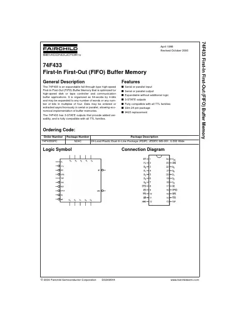
© 2000 Fairchild Semiconductor Corporation DS009544April 1988Revised October 200074F433 First-In First-Out (FIFO) Buffer Memory74F433First-In First-Out (FIFO) Buffer MemoryGeneral DescriptionThe 74F433 is an expandable fall-through type high-speed First-In First-Out (FIFO) Buffer Memory that is optimized for high-speed disk or tape controller and communication buffer applications. It is organized as 64-words by 4-bits and may be expanded to any number of words or any num-ber of bits in multiples of four. Data may be entered or extracted asynchronously in serial or parallel, allowing eco-nomical implementation of buffer memories.The 74F433 has 3-STATE outputs that provide added ver-satility, and is fully compatible with all TTL families.Featuress Serial or parallel input s Serial or parallel outputs Expandable without additional logic s 3-STATE outputss Fully compatible with all TTL families s Slim 24-pin package s 9423 replacementOrdering Code:Logic Symbol Connection DiagramOrder Number Package NumberPackage Description74F433SPCN24C24-Lead Plastic Dual-In-Line Package (PDIP), JEDEC MS-001, 0.300 Wide 274F 433Unit Loading/Fan OutBlock DiagramPin Names DescriptionU.L.Input I IH /I IL HIGH/LOW Output I OH /I OL PL Parallel Load Input 1.0/0.6620 µA/400 µA CPSI Serial Input Clock 1.0/0.6620 µA/400 µA IES Serial Input Enable 1.0/0.6620 µA/400 µA TTS Transfer to Stack Input 1.0/0.6620 µA/400 µA MR Master Reset 1.0/0.6620 µA/400 µA OES Serial Output Enable 1.0/0.6620 µA/400 µA TOP Transfer Out Parallel 1.0/0.6620 µA/400 µA TOS Transfer Out Serial 1.0/0.6620 µA/400 µA CPSO Serial Output Clock 1.0/0.6620 µA/400 µA OE Output Enable 1.0/0.6620 µA/400 µA D 0–D 3Parallel Data Inputs 1.0/0.6620 µA/400 µA D S Serial Data Input 1.0/0.6620 µA/400 µA Q 0–Q 3Parallel Data Outputs 285/10 5.7 mA/16 mA Q S Serial Data Output 285/10 5.7 µA/16 mA IRF Input Register Full 20/5400 µA/8 mA OREOutput Register Empty20/5400 µA/8 mA74F433Functional DescriptionAs shown in the block diagram, the 74F433 consists ofthree sections:1.An Input Register with parallel and serial data inputs,as well as control inputs and outputs for input hand-shaking and expansion.2. A 4-bit-wide, 62-word-deep fall-through stack with self-contained control logic.3.An Output Register with parallel and serial data out-puts, as well as control inputs and outputs for output handshaking and expansion.These three sections operate asynchronously and are vir-tually independent of one another.Input Register (Data Entry)The Input Register can receive data in either bit-serial or 4-bit parallel form. It stores this data until it is sent to the fall-through stack, and also generates the necessary status and control signals.This 5-bit register (see Figure 1) is initialized by setting flip-flop F 3 and resetting the other flip-flops. The Q-output ofthe last flip-flop (FC) is brought out as the Input Register Full (IRF) signal. After initialization, this output is HIGH.Parallel Entry —A HIGH on the Parallel Load (PL) input loads the D 0–D 3 inputs into the F 0–F 3 flip-flops and sets the FC flip-flop. This forces the IRF output LOW, indicating that the input register is full. During parallel entry, the Serial Input Clock (CPSI) input must be LOW.Serial Entry —Data on the Serial Data (D S ) input is serially entered into the shift register (F 3, F 2, F 1, F 0, FC) on each HIGH-to-LOW transition of the CPSI input when the Serial Input Enable (IES) signal is LOW. During serial entry, the PL input should be LOW.After the fourth clock transition, the four data bits are located in flip-flops F 0–F 3. The FC flip-flop is set, forcing the IRF output LOW and internally inhibiting CPSI pulses from affecting the register. Figure 2 illustrates the final posi-tions in an 74F433 resulting from a 256-bit serial bit train (B 0 is the first bit, B 255 the last).FIGURE 1. Conceptual Input Section 474F 433Functional Description (Continued)FIGURE 2. Final Positions in an 74F433Resulting from a 256-Bit Serial TrainFall-Through Stack —The outputs of flip-flops F 0–F 3 feed the stack. A LOW level on the Transfer to Stack (TTS) input initiates a fall-through action; if the top location of the stack is empty, data is loaded into the stack and the input register is re-initialized. (Note that this initialization is delayed until PL is LOW). Thus, automatic FIFO action is achieved by connecting the IRF output to the TTS input.An RS-type flip-flop (the initialization flip-flop) in the control section records the fact that data has been transferred to the stack. This prevents multiple entry of the same word into the stack even though IRF and TTS may still be LOW;the initialization flip-flop is not cleared until PL goes LOW.Once in the stack, data falls through automatically, pausing only when it is necessary to wait for an empty next location.In the 74F433, the master reset (MR) input only initializes the stack control section and does not clear the data.Output RegisterThe Output Register (see Figure 3) receives 4-bit data words from the bottom stack location, stores them, and out-puts data on a 3-STATE, 4-bit parallel data bus or on a 3-STATE serial data bus. The output section generates and receives the necessary status and control signals.Parallel Extraction —When the FIFO is empty after a LOW pulse is applied to the MR input, the Output Register Empty (ORE) output is LOW. After data has been entered into the FIFO and has fallen through to the bottom stack location, it is transferred into the output register, if the Transfer Out Parallel (TOP) input is HIGH. As a result of the data trans-fer, ORE goes HIGH, indicating valid data on the data out-puts (provided that the 3-STATE buffer is enabled). The TOP input can then be used to clock out the next word.When TOP goes LOW, ORE also goes LOW, indicating that the output data has been extracted; however, the data itself remains on the output bus until a HIGH level on TOP permits the transfer of the next word (if available) into the output register. During parallel data extraction, the serial output clock (CPSO) line should be LOW. The Transfer Out Serial (TOS) line should be grounded for single-slice oper-ation or connected to the appropriate ORE line for expanded operation (refer to the “Expansion ” section).The TOP signal is not edge-triggered. Therefore, if TOP goes HIGH before data is available from the stack but data becomes available before TOP again goes LOW, that data is transferred into the output register. However, internal control circuitry prevents the same data from being trans-ferred twice. If TOP goes HIGH and returns to LOW before data is available from the stack, ORE remains LOW, indi-cating that there is no valid data at the outputs.Serial Extraction —When the FIFO is empty after a LOW is applied to the MR input, the ORE output is LOW. After data has been entered into the FIFO and has fallen through to the bottom stack location, it is transferred into the output register, if the TOS input is LOW and TOP is HIGH. As a result of the data transfer, ORE goes HIGH, indicating that valid data is in the register.The 3-STATE Serial Data Output (Q S ) is automatically enabled and puts the first data bit on the output bus. Data is serially shifted out on the HIGH-to-LOW transition of CPSO. To prevent false shifting, CPSO should be LOW when the new word is being loaded into the output register.The fourth transition empties the shift register, forces ORE LOW, and disables the serial output, Q S . For serial opera-tion, the ORE output may be tied to the TOS input, request-ing a new word from the stack as soon as the previous one has been shifted out.ExpansionVertical Expansion —The 74F433 may be vertically expanded, without external components, to store more words. The interconnections necessary to form a 190-word by 4-bit FIFO are shown in Figure 4. Using the same tech-nique, any FIFO of (63n +1)-words by 4-bits can be config-ured, where n is the number of devices. Note that expansion does not sacrifice any of the 74F433 flexibility for serial/parallel input and output. 74F433Functional Description (Continued)FIGURE 3. Conceptual Output Section674F 433Functional Description(Continued)FIGURE 4. A Vertical Expansion SchemeHorizontal Expansion —The 74F433 can be horizontally expanded, without external logic, to store long words (in multiples of 4-bits). The interconnections necessary to form a 64-word by 12-bit FIFO are shown in Figure 5. Using the same technique, any FIFO of 64-words by 4n-bits can be constructed, where n is the number of devices.The right-most (most significant) device is connected to the TTS inputs of all devices. Similarly, the ORE output of the most significant device is connected to the TOS inputs of all devices. As in the vertical expansion scheme, horizontal expansion does not sacrifice any of the 74F433 flexibility for serial/parallel input and output.It should be noted that the horizontal expansion scheme shown in Figure 5 exacts a penalty in speed.Horizontal and Vertical Expansion —The 74F433 can be expanded in both the horizontal and vertical directions without any external components and without sacrificing any of its FIFO flexibility for serial/parallel input and output.The interconnections necessary to form a 127-word by 16-bit FIFO are shown in Figure 6. Using the same technique,any FIFO of (63m +1)-words by 4n-bits can be configured,where m is the number of devices in a column and n is the number of devices in a row. Figure 7 and Figure 8 illustrate the timing diagrams for serial data entry and extraction for74F433Functional Description (Continued)the FIFO shown in Figure 6. Figure 9 illustrates the final positions of bits in an expanded 74F433 FIFO resulting from a 2032-bit serial bit train.Interlocking Circuitry —Most conventional FIFO designs provide status signal analogous to IRF and ORE. However,when these devices are operated in arrays, variations in unit-to-unit operating speed require external gating to ensure that all devices have completed an operation. The 74F433 incorporates simple but effective 'master/slave'interlocking circuitry to eliminate the need for external gat-ing.In the 74F433 array of Figure 6, devices 1 and 5 are the row masters; the other devices are slaves to the master in their rows. No slave in a given row initializes its input regis-ter until it has received a LOW on its IES input from a row master or a slave of higher priority.Similarly, the ORE outputs of slaves do not go HIGH until their inputs have gone HIGH. This interlocking scheme ensures that new input data may be accepted by the array when the IRF output of the final slave in that row goes HIGH and that output data for the array may be extracted when the ORE output of the final slave in the output row goes HIGH.The row master is established by connecting its IES input to ground, while a slave receives its IES input from the IRF output of the next-higher priority device. When an array of 74F433 FIFOs is initialized with a HIGH on the MR inputs of all devices, the IRF outputs of all devices are HIGH.Thus, only the row master receives a LOW on the IES input during initialization.Figure 10 is a conceptual logic diagram of the internal cir-cuitry that determines master/slave operation. When MR and IES are LOW, the master latch is set. When TTS goes LOW, the initialization flip-flop is set. If the master latch is HIGH, the input register is immediately initialized and the initialization flip-flop reset. If the master latch is reset, the input register is not initialized until IES goes LOW. In array operation, activating TTS initiates a ripple input register ini-tialization from the row master to the last slave.A similar operation takes place for the output register.Either a TOS or TOP input initiates a load-from-stack oper-ation and sets the ORE request flip-flop. If the master latch is set, the last output register flip-flop is set and the ORE line goes HIGH. If the master latch is reset, the ORE output is LOW until a Serial Output Enable (OES) input is received.FIGURE 5. A Horizontal Expansion Scheme 874F 433Functional Description (Continued)FIGURE 6. A 127 x 16 FIFO ArrayFIGURE 7. Serial Data Entry for Array of Figure974F433Functional Description (Continued)FIGURE 8. Serial Data Extraction for Array of FigureFIGURE 9. Final Position of a 2032-Bit Serial InputFIGURE 10. Conceptual Diagram, Interlocking Circuitry 1074F 433Absolute Maximum Ratings (Note 1)Recommended Operating ConditionsNote 1: Absolute maximum ratings are values beyond which the device may be damaged or have its useful life impaired. Functional operation under these conditions is not implied.Note 2: Either voltage limit or current limit is sufficient to protect inputs.DC Electrical CharacteristicsStorage Temperature−65°C to +150°C Ambient Temperature under Bias −55°C to +125°C Junction Temperature under Bias −55°C to +150°C V CC Pin Potential to Ground Pin −0.5V to +7.0V Input Voltage (Note 2)−0.5V to +7.0V Input Current (Note 2)−30 mA to +5.0 mAVoltage Applied to Output in HIGH State (with V CC = 0V)Standard Output −0.5V to V CC 3-STATE Output −0.5V to +5.5VCurrent Applied to Output in LOW State (Max)twice the rated I OL (mA)Free Air Ambient Temperature 0°C to +70°CSupply Voltage+4.5V to +5.5VSymbol ParameterMin TypMaxUnits V CCConditionsV IH Input HIGH Voltage 2.0V Recognized as a HIGH Signal V IL Input LOW Voltage 0.8V Recognized as a LOW Signal V CD Input Clamp Diode Voltage −1.5VMin I IN = −18 mAV OHOutput HIGH 10% V CC 2.4VMinI OH = 400 µA (ORE, IRF)Voltage10% V CC 2.4I OH = 5.7 mA (Q n , Q s )5% V CC 2.7I OH = 400 µA (ORE, IRF)5% V CC2.7I OH = 5.7 mA (Q n , Q s )V OL Output LOW Voltage 10% V CC0.50V Min I OL = 16 mA (Q n , Q s )I IH Input HIGH Current 5.0µA Max V IN = 2.7V I BVI Input HIGH Current 7.0µA Max V IN = 7.0V Breakdown Test I CEX Output HIGH 50µA Max V OUT = V CC Leakage Current V ID Input Leakage 4.75V 0.0I ID = 1.9 µATestAll Other Pins Grounded I OD Output Leakage 3.75µA 0.0V IOD = 150 mVCircuit Current All Other Pins Grounded I IL Input LOW Current −0.4mA Max V IN = 0.5VI OZH Output Leakage Current 50µA Max V OUT = 2.7V (Q n , Q s )I OZL Output Leakage Current −50µA Max V OUT = 0.5V (Q n , Q s )I OS Output Short-Circuit Current −20−130mA Max V OUT = 0VI CCPower Supply Current150215mAMax74F433AC Electrical CharacteristicsSymbolParameterT A = +25°CT A = 0°C to +70°C UnitsFigure NumberV CC = +5.0V V CC = +5.0V C L = 50 pF C L = 50 pF MinMax Min Max t PHL Propagation Delay, Negative-Going 2.017.0 2.018.0nsFigures 11, 12CPSI to IRF Output t PLH Propagation Delay,9.034.08.038.0Negative-Going TTS to IRF t PLH Propagation Delay, Negative-Going 4.025.0 3.027.0ns Figures 13, 14t PHL CPSO to Q S Output5.020.0 5.021.0t PLH Propagation Delay, Positive-Going 8.035.07.038.0ns Figure 15t PHL TOP to Q 0–Q 3 Outputs 7.030.07.032.0t PHL Propagation Delay,7.025.0 6.028.0nsFigures 13, 14Negative-Going CPSO to ORE t PHL Propagation Delay,6.026.0 6.028.0nsFigure 15Negative-Going TOP to ORE t PLH Propagation Delay, Positive-Going 13.048.012.051.0TOP to OREt PLH Propagation Delay, Negative-Going 13.045.012.050.0nsFigures 13, 14TOS to Positive-Going ORE t PHL Propagation Delay, Positive- 4.022.0 4.023.0nsFigures 17, 18Going PL to Negative-Going IRF t PLH Propagation Delay, Negative-7.031.0 6.035.0Going PL to Positive-Going IRF t PLH Propagation Delay,9.038.08.044.0nsPositive-Going OES to ORE t PLH Propagation Delay Positive-IRF 5.025.0 5.027.0ns Figure 18Going IES to Positive-Going t PHL Propagation Delay 7.028.07.031.0ns MR to ORE t PLH Propagation Delay 5.027.0 5.030.0nsMR to IRF t PZH Enable Time 1.016.0 1.018.0nst PZL OE to Q 0–Q 3 1.014.0 1.016.0t PHZ Disable Time 1.010.0 1.012.0t PLZ OE to Q 0–Q 3 1.023.0 1.030.0t PZH Enable Time1.010.0 1.012.0nst PZL Negative-Going OES to Q S 1.014.0 1.015.0t PHZ Disable Time1.010.0 1.012.0t PLZ Negative-Going OES to Q S 1.014.0 1.016.0t PZH Enable Time 1.035.0 1.042.0ns t PZL TOS to Q S1.035.0 1.039.0t DFT Fall-Through Time 0.20.90.2 1.0nsFigure 16t AP Parallel Appearance Time −20.0−2.0−20.0−2.0nsORE to Q 0–Q 3t ASSerial Appearance Time −20.05.0−20.05.0ORE to Q S 1274F 433AC Operating RequirementsSymbol ParameterT A = +25°CT A = 0°C to +70°C UnitsFigure NumberV CC = +5.0V V CC = +5.0V Min MaxMin Maxt S (H)Setup Time, HIGH or LOW 7.07.0nsFigures 11, 12t S (L)D S to Negative CPSI 7.07.0t H (H)Hold Time, HIGH or LOW 2.0 2.0t H (L)D S to CPSI2.02.0t S (L)Setup Time, LOW TTS to IRF,0.00.0nsFigures 11, 12, 17,18Serial or Parallel Modet S (L)Setup Time, LOW Negative-Going 0.00.0nsFigures 13, 14ORE to Negative-Going TOS t S (L)Setup Time, LOW Negative-Going 8.09.0nsFigure 12IES to CPSIt S (L)Setup Time, LOW Negative-Going 30.033.0TTS to CPSIt S (H)Setup Time, HIGH or LOW 0.00.0nst S (L)Parallel Inputs to PL 0.00.0t H (H)Hold Time, HIGH or LOW 4.0 4.0t H (L)Parallel Inputs to PL 4.0 4.0t W (H)CPSI Pulse Width 10.011.0ns Figures 11, 12t W (L)HIGH or LOW 5.0 6.0t W (H)PL Pulse Width, HIGH 7.09.0ns Figures 17, 18t W (L)TTS Pulse Width, LOW 7.09.0ns Figures 11, 12, 13,14Serial or Parallel Modet W (L)MR Pulse Width, LOW 7.09.0ns Figure 16t W (H)TOP Pulse Width 14.016.0nsFigure 15t W (L)HIGH or LOW 7.07.0t W (H)CPSO Pulse Width 14.016.0ns Figures 13, 14t W (L)HIGH or LOW 7.07.0t RECRecovery Time 8.015.0nsFigure 16MR to Any Input74F433Timing WaveformsConditions: Stack not full, IES, PL LOWFIGURE 11. Serial Input, Unexpanded or Master OperationConditions: Stack not full, IES HIGH when initiated, PL LOWFIGURE 12. Serial Input, Expanded Slave OperationConditions: Data in stack, TOP HIGH, IES LOW when initiated, OES LOWFIGURE 13. Serial Output, Unexpanded or Master Operation 1474F 433Timing Waveforms (Continued)Conditions: Data in stack, TOP HIGH, IES HIGH when initiatedFIGURE 14. Serial Output, Slave OperationConditions: IES LOW when initiated, OE, CPSO LOW; data available in stackFIGURE 15. Parallel Output, 4-Bit Word or Master in Parallel ExpansionConditions: TTS connected to IRF, TOS connected to ORE, IES, OES, OE, CPSO LOW, TOP HIGHFIGURE 16. Fall Through Time74F433Timing Waveforms (Continued)Conditions: Stack not full, IES LOW when initializedNOTE A: TTS normally connected to IRF.NOTE B: If stack is full, IRF will stay LOW.FIGURE 17. Parallel Load Mode, 4-Bit Word (Unexpanded) or Master in Parallel ExpansionConditions: Stack not full, device initialized (Note 3) with IES HIGHNote 3: Initialization requires a master reset to occur after power has been applied.FIGURE 18. Parallel Load, Slave Mode1674F 433 F i r s t -I n F i r s t -O u t (F I F O ) B u f f e r M e m o r yPhysical Dimensions inches (millimeters) unless otherwise noted24-Lead Plastic Dual-In-Line Package (PDIP), JEDEC MS-001, 0.300 WidePackage Number N24CFairchild does not assume any responsibility for use of any circuitry described, no circuit patent licenses are implied and Fairchild reserves the right at any time without notice to change said circuitry and specifications.LIFE SUPPORT POLICYFAIRCHILD ’S PRODUCTS ARE NOT AUTHORIZED FOR USE AS CRITICAL COMPONENTS IN LIFE SUPPORT DEVICES OR SYSTEMS WITHOUT THE EXPRESS WRITTEN APPROVAL OF THE PRESIDENT OF FAIRCHILD SEMICONDUCTOR CORPORATION. As used herein:1.Life support devices or systems are devices or systems which, (a) are intended for surgical implant into the body, or (b) support or sustain life, and (c) whose failure to perform when properly used in accordance with instructions for use provided in the labeling, can be rea-sonably expected to result in a significant injury to the user. 2. A critical component in any component of a life support device or system whose failure to perform can be rea-sonably expected to cause the failure of the life support device or system, or to affect its safety or effectiveness.。
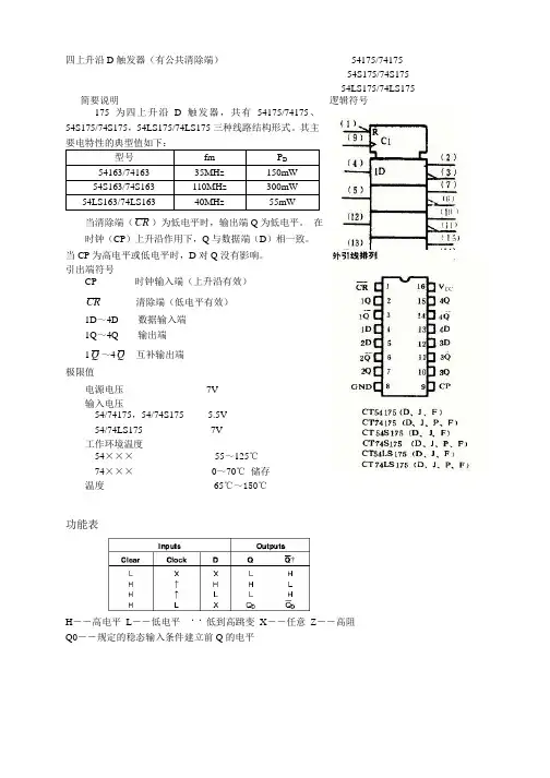
四上升沿D 触发器(有公共清除端)54175/7417554S175/74S17554LS175/74LS175逻辑符号简要说明175 为四上升沿 D 触发器,共有54175/74175 、54S175/74S175,54LS175/74LS175 三种线路结构形式。
其主要电特性的典型值如下:型号fm P D54163/7416335MHz150mW54S163/74S163110MHz300mW54LS163/74LS16340MHz55mW当清除端(CR )为低电平时,输出端Q 为低电平。
在时钟(CP)上升沿作用下,Q 与数据端(D)相一致。
当CP 为高电平或低电平时,D 对Q 没有影响。
引出端符号CP 时钟输入端(上升沿有效)CR 清除端(低电平有效)1D~4D 数据输入端1Q~4Q 输出端1 Q ~4 Q 互补输出端极限值电源电压7V输入电压54/74175,54/74S175 5.5V54/74LS175 7V工作环境温度54×××-55~125℃74×××0~70℃储存温度-65℃~150℃功能表H――高电平L――低电平‘‘低到高跳变X――任意Z――高阻Q0――规定的稳态输入条件建立前Q 的电平54/7417554/74S17554/74LS175单位最小额定最大最小额定最大最小额定最大电源电压V CC54 4.55 5.5 4.55 5.5 4.55 4.5V74 4.755 5.25 4.755 5.25 4.755 5.25输入高电平电压V iH222V输入低电平电压V iL 540.80.80.7V 740.80.80.8输出高电平电流I OH-800-1000-400uA 输出低电平电流I OL5416304mA 7416308时钟频率fcp025075030MHz 脉冲宽度T W CP20725ns CR201020ns建立时间t setD20520ns CR 无效态25520ns保持时间t H530ns 逻辑图[2]: fmax 最大时钟频率。
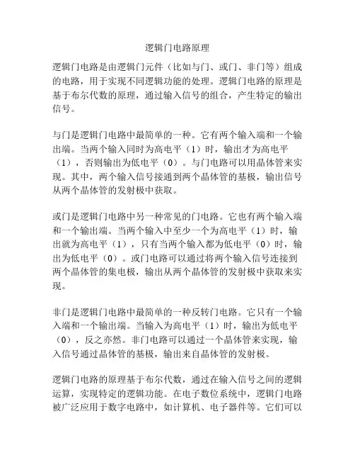
逻辑门电路原理
逻辑门电路是由逻辑门元件(比如与门、或门、非门等)组成的电路,用于实现不同逻辑功能的处理。
逻辑门电路的原理是基于布尔代数的原理,通过输入信号的组合,产生特定的输出信号。
与门是逻辑门电路中最简单的一种。
它有两个输入端和一个输出端。
当两个输入同时为高电平(1)时,输出才为高电平(1),否则输出为低电平(0)。
与门电路可以用晶体管来实现。
其中,两个输入信号接通到两个晶体管的基极,输出信号从两个晶体管的发射极中获取。
或门是逻辑门电路中另一种常见的门电路。
它也有两个输入端和一个输出端。
当两个输入中至少一个为高电平(1)时,输出就为高电平(1),只有当两个输入都为低电平(0)时,输出为低电平(0)。
或门电路可以通过将两个输入信号连接到两个晶体管的集电极,输出从两个晶体管的发射极中获取来实现。
非门是逻辑门电路中最简单的一种反转门电路。
它只有一个输入端和一个输出端。
当输入为高电平(1)时,输出为低电平(0),反之亦然。
非门电路可以通过一个晶体管来实现,输入信号通过晶体管的基极,输出来自晶体管的发射极。
逻辑门电路的原理基于布尔代数,通过在输入信号之间的逻辑运算,实现特定的逻辑功能。
在电子数位系统中,逻辑门电路被广泛应用于数字电路中,如计算机、电子器件等。
它们可以
实现逻辑运算、信号控制、数据存储等功能,是现代电子设备中不可或缺的一部分。


无论多么复杂的单片机电路,都是由若干基本电路单元组成的。
2.2.1 常用的逻辑门电路最基本的门电路是与、或、非门,把它们适当连接可以实现任意复杂的逻辑功能。
用小规模集成电路构成复杂逻辑电路时,最常用的门电路是与(AND)、或(OR)、非(INV BUFF)、恒等(BUFF)、与非(NAND)、或非(NOR)、异或(XOR)。
主要是因为这7种电路既可以完成基本逻辑功能,又具有较强的负载驱动能力,便于完成复杂而又实用的逻辑电路设计。
1.与门与门是一个能够实现逻辑乘运算的、多端输入、单端输出的逻辑电路,逻辑函数式:F = A·B其记忆口诀为:有0出0,全1才1。
2.或门或门是一个能够实现逻辑加运算的多端输入、单端输出的逻辑电路,逻辑函数式:F = A+B其记忆口诀为:有1出1,全0才0。
3.非门实现非逻辑功能的电路称为非门,有时又叫反相缓冲器。
非门只有一个输入端和一个输出端,逻辑函数式是:F =A非非门逻辑符号4.恒等门实现恒等逻辑功能的电路称为恒等门,又叫同相缓冲器。
恒等门只有一个输入端和一个输出端,逻辑函数式是:F = A同相缓冲器和反相缓冲器在数字系统中用于增强信号的驱动能力。
5.与非门与和非的复合运算称为与非运算,逻辑函数式是:F = A.B非其记忆口诀为:有0出1,全1才0。
6.或非门或与非的复合运算称为或非运算,逻辑函数式是:F = A+B非其记忆口诀为:有1出0,全0才1。
7.异或门异或逻辑也是一种广泛应用的复合逻辑,其记忆口诀为:相同出0,不同出1。
逻辑门电路是单片机外围电路运算、控制功能所必需的电路。
在单片机系统中我们经常使用集成逻辑电路(常称为集成电路)。
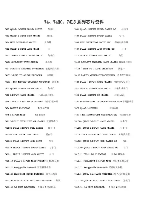
一片集成逻辑门电路中通常含有若干个逻辑门电路,如7400为4重二输入与非门,即7400内部有4个二输入的与非门。
高速CMOS74HC逻辑系列集成电路具有低功耗、宽工作电压、强抗干扰的特性,是单片机外围通用集成电路的首选系列。