XFAB_Cadence_PDK_Install_Guide
- 格式:ppt
- 大小:4.26 MB
- 文档页数:29

第一章.Cadence cdsSPICE的使用说明Cadence cdsSPICE 也是众多使用SPICE内核的电路模拟软件之一。
因此他在使用上会有部分同我们平时所用到的PSPICE相同。
这里我将侧重讲一下它的一些特殊用法。
§ 1-1 进入Cadence软件包一.在工作站上使用在命令行中(提示符后,如:ZUEDA22>)键入以下命令icfb&↙(回车键),其中& 表示后台工作。
Icfb调出Cadence软件。
出现的主窗口如图1-1-1所示:图1-1-1Candence主窗口二.在PC机上使用1)将PC机的颜色属性改为256色(这一步必须);2)打开Exceed软件,一般选用xstart软件,以下是使用步骤:start method选择REXEC(TCP-IP) ,Programm选择Xwindow。
Host选择10.13.71.32 或10.13.71.33。
host type选择sun。
并点击后面的按钮,在弹出菜单中选择command tool。
确认选择完毕后,点击run!3)在提示符ZDASIC22> 下键入:setenv DISPLAY 本机ip:0.0(回车)4)在命令行中(提示符后,如:ZUEDA22>)键入以下命令icfb&↙(回车键)即进入cadence中。
出现的主窗口如图1-1-1所示。
以上是使用xstart登陆cadance的方法。
在使用其他软件登陆cadance时,可能在登录前要修改文件.cshrc,方法如下:在提示符下输入如下命令:vi .cshrc↙(进入全屏幕编辑程序vi)将光标移至setevn DISPLAY ZDASIC22:0.0 处,将“ZDASIC22”改为PC机的IP,其它不变(重新回到服务器上运行时,还需按原样改回)。
改完后存盘退出。
然后输入如下命令:source .cshrc↙(重新载入该文件)以下介绍一下全屏幕编辑程序vi的一些使用方法:vi使用了两种状态,一是指令态(Command Mode),另一是插入态(Insert Mode)。
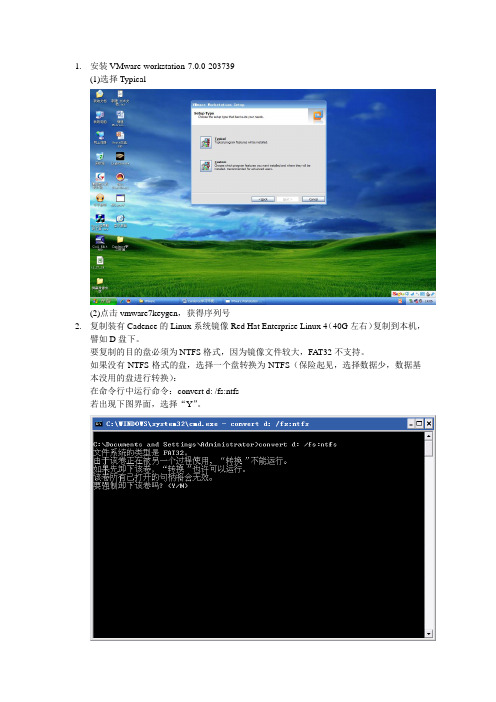
1.安装VMware-workstation-7.0.0-203739(1)选择Typical(2)点击vmware7keygen,获得序列号2.复制装有Cadence的Linux系统镜像Red Hat Enterprise Linux 4(40G左右)复制到本机,譬如D盘下。
要复制的目的盘必须为NTFS格式,因为镜像文件较大,FAT32不支持。
如果没有NTFS格式的盘,选择一个盘转换为NTFS(保险起见,选择数据少,数据基本没用的盘进行转换):在命令行中运行命令:convert d: /fs:ntfs若出现下图界面,选择“Y”。
3.用VMware-workstation打开Linux镜像:D:\Red Hat Enterprise Linux 4点击“Open Existing VM or Team”,打开D:\Red Hat Enterprise Linux 4\Red Hat Enterprise Linux 4.vmx。
点击左侧的“Power on this Virtual Machine”,打开虚拟机。
选择“I copied it”。
用户名:ciomp密码:123456用Ctrl+Alt,可以实现鼠标在虚拟机和宿主xp之间切换。
4.设置宿主主机的IP为10.1.2.*子网掩码:255.255.255.0网关:10.1.2.1注意各练习机IP发生相互冲突!5.在虚拟机内ping下Cadence License Server(IP为10.1.2.254),测试连通性:在虚拟机的桌面点击右键,选择“Open Terminal”,在弹出的命令窗口内键入:ping 10.1.2.254。

Ubuntu18.04安装配置CadenceVirtuoso617之前的Centos7为了使⽤spectre提供的matlab toolbox,结果不⼩⼼删除了/usr/lib64中的某些动态库(XXXX.so⽂件),导致重启之后内核崩溃。
这⾥送上忠告:尽量不要使⽤rm命令,使⽤mv命令改名备份最好。
于是进⼊了“漫长”的拯救数据⾏动,这⾥只给出主要思路:由于清楚问题出现的原因,我⾸先是通过安装盘(U盘)进⼊拯救模式,然后拷贝了U盘核⼼中的动态库到原系统的动态库。
此时原系统可以进⼊终端模式,但进⼊图形界⾯时登陆账户后就⿊屏且重新回到登陆界⾯,并且终端中不能联⽹,也⽆法重新安装系统核⼼。
看来系统应该很难救回来了,于是使⽤终端将关键数据进⾏打包,并挂载上移动硬盘将数据拷贝出来,此时数据拯救成功。
Centos系统虽已稳定著称,但同时也是个磨⼈的⼩妖精:常常为了解决各种依赖⽽耗费⼤量时间。
因此决定转向⽀持更完善的Ubuntu系统,⽬前的使⽤证明Ubuntu是个⽼⼤哥,不再是⼩妖精了。
Ubuntu的官⽅库完善,且在国内也能愉快地下载,再加上⽹络上已有很多Ubuntu安装Virtuoso的教程,因此Ubuntu是个不错的选择。
安装Ubuntu18.04在Win下进⼊官⽹下载,并制作安装U盘。
建议使⽤,点击即可下载。
教程较多,不再赘述。
安装Ubuntu,我的分区如下(双系统)挂载点功能⼤⼩设置swap内存交换空间12G主分区、空间起始位置/boot内核及引导⽂件位置1G逻辑分区、空间起始位置、EXT4/根⽬录40G主分区、空间起始位置、EXT4/opt第三⽅软件安装⽬录(⾃⾏安装)100G逻辑分区、空间起始位置、EXT4/usr官⽅软件安装⽬录100G逻辑分区、空间起始位置、EXT4/home⽤户⽬录,存储数据800G逻辑分区、空间起始位置、EXT4更新内核、软件、驱动# 更新软件库sudo apt-get update# 更新软件sudo apt-get upgrade# 更新系统sudo apt-get dist-upgrade# ⾃动更新、下载驱动(可以⾃动安装Nvidia驱动,⽅便快捷)sudo ubuntu-drivers autoinstall安装、配置Cadence Virtuoso不是真正的安装,是将我Centos系统中的Cadence软件库打包并解压过来的,真正的安装过程其他的博客讲的很清楚啦。

PDK压缩文件解压后有安装引导文件,其文件名里有类似于setup的字样,根据系统不同可以双击运行或者在终端中运行,输入要安装的目标目录路径,一般就是你要在其中工作而建的目录(比如自己在用户主目录下建了一个名字为ic1的目录),之后能在此目录的子目录下看到若干个文件夹,如libs,models,docs,skill,tech。
stream之类的文件目录,还有个cds.lib文件,其中libs目录里就是元件库,各个元件的库下一般有symbol,layout,spectre,hspice等文件夹。
把cds.lib文件和tech目录下的display.drf和tech.tf文件一定拷贝到你建的工作目录ic1下,然后最好把cds.lib里的库的路径改成绝对路径,包括cadence自带的analoglib,basic等库的路径都改成绝对路径,好像还有一个隐藏文件也要拷贝过来,你可以看看docs目录里的文档,应该比我说的详细。
在终端窗口中进入ic1目录后,再输入icfb &启动cadence,就应该可以了。
新建自己的设计库要关联ASCII的technology file文件,直接关联到上边的tech.tf就可以了至于没有PDK文件的,在建好自己的工作目录(比如上面说的ic1)后,就要手动拷贝cds.lib到ic1目录下,在cadence的安装目录里有好多现成的cds.lib文件,在candence安装目录下的/tools/dfII/etc/cdsDotLibs/目录下就有好多,自己拷贝一个后,可以把其它cds.lib文件里定义的库的路径粘贴到你拷贝到ic1下的cds.lib文件里,记得把路径改成绝对路径,比如cadence安装目录下的/tools/dfII/etc/cdslib/artist/analogLib就是analogLib库的路径。
之后进入ic1下启动cadence,应该就可以了,画原理图和仿真,把仿真的model也可以拷贝到ic1下,方便。

1Synopsys工具的安装1.1 文件结构安装CentOS 4.5操作系统,选择安装成server,在安装过程中选择全部安装,语言采用ENGLISH。
在安装之前,需要有个很好的文件管理结构,将所有的EDA工具按照有效的文件结构安装,并且有效的管理license。
文件结构图如下:在根目录下建立CAD,用来保存所有的安装工具1.2 DC工具安装DC安装文件是syn_v2006.06,使用synopsysinstaller安装文件启动安装程序。
在普通用户下解压DC安装文件里面的压缩文件,一共两个文件:syn_v2006.06-SP6-20070820_amd64.tar和syn_v2006.06-SP6-20070820_common.tar。
同时,解压synopsysinstaller文件里的installer_v1.6.tar,该文件含有安装程序。
在synopsysinstaller目录下,使用命令行输入“./setup.sh”打开安装界面,按照如下图所示的安装步骤一步一步安装即可完成。
1.3 安装primetime和formalitypt_vZ-2007.06-SP3-3是pt工具,用于静态时序分析,fm_vZ-2007.06是formality工具,用于形式验证。
这些安装根据synopsysinstaller的引导一步步安装就可以了,和DC的安装一样,过程完全一样,在这里不再解释。
1.4 安装synopsys的SOLD用户使用手册SOLD用户使用手册的安装文件是SOLD-2007.03.tar.zip,将其解压得到SOLD-2007.03文件夹,解压你所要安装的目录,即可使用。
要想阅读SOLD,还需要安装pdf阅读器,使用AdobeReader_enu-7.0.1-1.i386.rpm安装文件,双击即可完成安装。
1.5 Synopsys工具的破解首先要添加一个普通用户,该用户用于安装及使用各种EDA工具,不推荐使用root用户进行安装和运行。

Cadence IC Design ManualFor EE5518ZHENG Huan QunLin Long YangRevised onMay 2017Department of Electrical & Computer EngineeringNational University of SingaporeContents1 INTRODUCTION (4)1.1 Overview of Design Flow (4)1.2 Getting Started with Cadence (6)1.3 Using Online Help (8)1.4 Exit Cadence (8)2 SCHEMATIC ENTRY (9)2.1 Creating a New Design Library (9)2.2 Creating a Schematic Cellview (10)2.3 Adding Components to Schematic (11)2.4 Adding Pins to Schematic (12)2.5 Adding Wires to Schematic (13)2.6 Saving Your Design (14)3 SYMBOL AND TEST CIRCUIT CREATION (15)3.1 Creating Symbol (15)3.2 Editing Symbol (16)3.3 Building Test Bench (18)4 SIMULATING YOUR CIRCUIT (21)4.1 Start the Simulation Environment (21)4.2 Selecting Project Directory (21)4.3 Setup Model Library (22)4.4 Choosing the Desired Analysis (22)4.5 Setup Variables (23)4.6 Saving Simulation Data (24)4.7 Saving Output for Plotting (24)4.8 Viewing the Netlists (25)4.9 Running the Simulation (25)5 PHYSICAL LAYOUT (28)5.1 Layout vs Symbol of CMOS Devices (28)5.2 Starting Layout Editor (29)5.3 Vias (31)5.4 Changing the Grid (33)5.5 Inserting and Editing Instances (34)5.6 Drawing Shapes / Paths (35)5.7 Creating Pins (36)6 DESIGN VERIFICATION: DRC AND LVS (38)6.1 Performing DRC (38)6.2 Performing LVS (40)6.3 Performing PEX (41)7 POST‐LAYOUT SIMULATION (45)7.1 Simulation the Extracted Cell View (45)8 CONCLUSION (46)1INTRODUCTIONThis manual describes how to use Cadence IC design tools. It covers the whole design cycle, from the front-end to the back-end, i.e., from the pre-layout design to the post-layout design.The manual aims to provide a guide for fresh users. Following the manual, users can start doing analog IC design even though the users don’t have any knowledge of the tools.An inverter is used to illustrate the whole cycle of analog IC design, and Cadence Generic 45nm (cg45nm) kit is the technology library used for implementing the inverter. The method stated in the manual can be applied to other type of analog circuit design.1.1Overview of Design FlowFigure 1 shows a typical analog IC design flow.The design flow starts from schematic entry with the Cadence schematic capture tool –Schematic Editor. Devices or cells from the cg45nm or other libraries are used to build your circuit. Your design is hierarchical; therefore higher level schematics also incorporate cells which you have already developed. The schematics which you enter at this stage therefore typically consist of a number of base library cells and also lower level cells designed yourself.These are described in Sections 2 and 3 of the manual.When you have finished designing a particular circuit, you need to simulate it to ensure that it works as expected. It would be unlikely that your circuit works as expected at the first time so you have to repeat the cycle to improve the circuit, as shown in Figure 1, until the circuit works satisfactorily. This must be done for each sub-circuit of your design and then for the top level design. How to simulate and view the performance of simulation results are presented in Sections 4 of the manual.When the performance of the circuit is satisfactory, it is ready to start the physical design or layout of the circuit. The layout starts with the cell or device placement. Once the cells have been placed, routing can be carried out. Routing connects the cells/device of the design.After finishing placement and routing, the layout has to go through the Design Rule Check (DRC) with rule decks provided by PDK provider, to ensure that there is no design rule violation in the layout. The layout has to be rectified accordingly to the rules’ requirement till it passes DRC.Upon a successful DRC, it is Layout-versus-Schematic (LVS) check, to assure that all connections in the layout are correct. The layout has to be amended accordingly to the schematic If LVS doesn’t pass. DRC has to be done whenever layout is changed. The process is repeated until the LVS passes.Figure 1. Analog IC Design FlowThe next step is parasitic extraction (PEX) to get the extracted view of the circuit, which is used for post–layout simulation. The extracted view includes the parasitic effects in both the instances/devices and the required wiring interconnects of the circuit.Following DRC, LVS and PEX, it is post-layout simulation. The post-layout simulation is essential to make sure that the circuit with the extra parasitic parameters functions well and still meet the design specifications. If the performance of the post-layout simulation is not acceptable, back to the stage of schematic entry to check the circuit. Basically, re-design the circuit is necessary. Repeat the whole flow until the results of the post-layout simulation meet the design specifications.If everything is satisfactory, the next stage is GDSII Generation. It generates a file which depicts the low level geometry of layout. GDSII format is industry standard format suitable fora semiconductor company to fabricate and manufacture the chip of layout. This is briefed inthe last section of the manual.1.2Getting Started with CadenceUpon logging into your account, you will be brought to the Linux Desktop Environment.Right click on the desktop and click Open Terminal to open a “window” on the desktop. This window is the Linux command line prompt at which you can run Linux commands. After running a Linux command, this window also shows the output of the command.The following steps show how to start Cadence with cg45nm kit.A.Create a working directory - project (it can be any name as you like) with thecommand:mkdir projectwhere mkdir is Linux command and the project is the directory name;B.Enter the working directory with the command:cd projectwhere the cd is the Linux command;C.Type the followings commands to do the environment setup for using Cadence Generic45nm PDK.cp /app11/cg45nm/USERS/cds.lib .cp /app11/cg45nm/USERS/assura_tech.lib .cp /app11/cg45nm/USERS/pvtech.lib .D.Start cadence in the working directory – project with the following command:virtuoso &where virtuoso is the command to start Cadence IC design tool.Now, Cadence tools are successfully started. Keeps only the Command Input Window (CIW) which is shown in Figure 2.Figure 2. CIW WindowDo not close this CIW and try to keep it in view whenever you are using Cadence. Error messages and output from some of the tools are always sent to the CIW. If something doesn't appear to be working, always check the CIW for error messages. In addition, the CIW allows the user great control over Cadence by interpreting skill commands which are typed into it.E.In the CIW, select Tools Library Manager. The Library Manager pop up as inFigure 3. The Library Manager is where you create, add, copy, delete and organizeyour libraries and cell views.Figure 3. Library Manager WindowYou can see that the library gpdk045 appears in the Library column of the librarymanager.Now, you have started Cadence tool and loaded the cg45nm kit successfully. There are some documents in /app11/cg45nm/ gpdk045_v4_0/docs, and you can always refer to these documents for the information such as devices, device models, DRC rules and others related to cg45nm kit.Next time, you need only to repeat the steps B and D, for launching Cadence virtuoso and doing your project.1.3Using Online HelpCadence provides a comprehensive online manuals for all Cadence tools. You can launch the online help by typing the following command at the Linux prompt.cdnshelpThis invokes the online software manuals. Alternately, there is a help menu on each Cadence window. Manual which is related to that window related will pop-up once clicking on the help button.1.4Exit CadenceTo exit Cadence, just click on the cross sign X or File Exit in CIW. It is necessary to exit Cadence when it is not in use. Your library file would be locked or cannot edited next time if Cadence was not exited properly.2SCHEMATIC ENTRYNow that Cadence is running, you are almost ready to start entering schematics. However, you must first create a library which will be used to store all the parts of your design. Then, schematic can be created in the library.2.1Creating a New Design LibraryA.In the Library Manager window, select File→New→Library. New Library formpops up as shown in Figure 4.B.In the New Library form referring to Figure 4, key in your design library name(example: test) in the field of Name, and then click Ok.C.Click Ok in the pop-up window - the Technology File for New Library, referring toFigure 5.D.Choose gpdk045 in the Attach Library to Technology Library form, referring toFigure 6, and then click Ok.Figure 4. New Library FormFigure 5. Technology File for New Library FormFigure 6. Attach Library to Technology File FormA new library, named test, should appear in your Library Manager window.2.2 Creating a Schematic CellviewA.In Library Manager, select the Library where you would like to create a schematic. Then,select File→New→Cell View.B.Set up the New File form as Figure 7Figure 7. Create CellViewC.Click OK when done. A blank schematic window for the "inv" (your cell name)schematic appears.Explore the functions available by putting your mouse over the toolbar and fixed menu icons.In addition, note that some of the menu selections have alphabets listed to the right of them. These are bind-key or shortcut-key definitions which are very useful in the long run.Test them out during the schematic drawing in subsequent steps.2.3Adding Components to SchematicFigure 8 shows the schematic which you are going to patch, and the property of each component is listed in Table 1.Figure 8. Inverter CircuitTabel 1. Component Properties of Figure 8: Inverter CircuitComponents Library Name Cell Name PropertiesPMOS gpdk045 pmos1v l:45nm w:120nm (default size)NMOS gpdk045 nmos1v l:45nm w:120nm (default size)Here is the example on how to add component instances by placing cell views from libraries. Type “i” bind-key or select Create Instance in the schematic window or click on the menu bar to display Add Instance form. Then in the Add Instance window, select gpdk045as Library, choose the NMOS transistor by selecting nmos1v in Cell and also choose symbol as View, as shown in Figure 9.Figure 9. Add Instance FormSimilarly, add the pmos1v into the schematic. As an example, here we just keep all theparameters as default.If you place a component with the wrong parameter values, select the component and type “q” bindkey or use the Edit→Properties→Objects command to change the parameters. Use the Edit→Move command or type “m” if you place components in the wrong location.2.4Adding Pins to SchematicYou must place I/O pins in your schematic to identify the inputs and the outputs. A pin can be an input, output or an input-output (bi-directional) pin.Type “p” or select Add →Pin from inv Schematic Window or click the Pin fixed menuicon in the schematic window. The Add Pin form appears as Figure 10.Figure 10. Add Pin FormClick Hide and move you cursor to the Schematic Window. Place pins at the correct places and click right mouse key to rotate the pin if necessary.Add pins according to Table 2, paying attention to the direction.Table 2. Pin Names and Direction of invPin Names DirectionVin InputVout OutputVDD, GND Input-OutputCaution: Do not use the add component form to place schematic pins.2.5 Adding Wires to SchematicAdd wires to connect the components and pins in the design.A.Type “w” or select Add →Wire (narrow) in Schematic Window or click (narrow)fixed menu icon.B.In the schematic window, click on a pin of one of your components as the first pointfor your wiring. A diamond shape appears over the starting point of this wire.C.Follow the prompts at the bottom of the design window and click left mouse key onthe destination point for your wire.D.Continue wiring the schematic. When done wiring, press Esc with your cursor in theschematic window to cancel wiring.2.6Saving Your DesignCheck the design to ensure that it is correct and save the design.A.Click the Check and Save icon in the schematic window.B.Observe the CIW output area, for the information of the check and save action.3SYMBOL AND TEST CIRCUIT CREATIONSymbols are useful when creating designs as it is impractical to show every transistor on the top level schematic. Instead, the symbols of cells are created in order to instantiate them in the higher level schematics and make them more readable (i.e. hierarchical designs). Create a symbol for your design so you can place it in a test circuit for simulation.3.1Creating SymbolA.In the inv schematic window, select Create → Cellview → From Cellview. CellviewFrom Cellview pops up as shown in Figure 11.Figure 11. Cellview From Cellview FormB.Click OK in the Cellview From Cellview form. The Symbol Generation Options formappears as Figure 12. Enter the information listed in Table 3 for the symbol.Table 3: Pin SpectificationsLeft Pins : VinRight Pins : VoutTop Pins: VDDBottom Pins: GNDFigure 12. Symbol Generation Options FormC.Click OK in the Symbol Generation Options form. A window with a symbol createdautomatically by the tools pops up, referring to Figure 13.Figure 13. Symbol Generated AutomaticallyD.Observe the CIW output pane and note the messages stating Adding ‘CDFinformation ...’.3.2Editing SymbolYou can modify the symbol to have a more meaningful shape for easy recognition.A.Move your cursor over the symbol, until the entire green rectangle is highlighted. Clickleft to select it.B.Click Delete icon in the symbol window to delete the green rectangle.C.Select Create→Shape→Polygon. Follow the prompts at the bottom of the symbol, anddraw the triangle shown in Figure 14.D.Type “m” or click Move icon in the symbol window, move the pins to the finaldestination.E.Select [@partName], and use Edit→Properties→Object to change it to inverter asshown in Figure 14.Figure 14. Edit Object Properties FormF.Save your edited symbol view. The final symbol is shown in Figure 15.Figure 15. Symbol of inv3.3Building Test BenchTo test the inverter that you have just built, you need to create a test bench. This test bench will also be used during the post-layout simulation.Creating an inv_test schematic cellview with the below information, following the steps listed in Section 2 – SCHEMATIC ENTRY. The test bench is as shown in Figure 17.Library Name : testCell Name : inv_testView Name : schematicLibrary Name Cell Name Propertiestest inv_testanalogLib Vdc VDDanalogLib vpulse Referring to Figure 16analogLib gnd GNDanalogLib cap 1f FFigure 16. Vpulse FormFigure 17. Test Bench – inv_test for inv CircuitNote:There are wire names Vin and Vout in Figure 17. These can be created by clicking on Create Wire Name on the inv_test schematic window. Key in Vin Vout in the Names field of the Add Wire Name form, and then click Hide. Moving your mouse to the schematic window, click the wire where you want it to be named in the same sequence as typing the names in the Names field.4SIMULATING YOUR CIRCUITBefore starting the simulation, make sure that the schematic (inv_test) is open, then perform the following steps.4.1Start the Simulation EnvironmentIn your schematic window, select Launch →ADE L. The Analog Design Environment (ADE) window appears as shown in Figure 18.Figure 18. ADE Window4.2Selecting Project DirectoryIn the ADE window, select Setup→Simulator/ Directory/ Host. A Choosing Simulator form appears as Figure 19. In the Project Directory blank, type in /var/tmp/(desired folder name) to save your simulation files in the /var/tmp directory on the local server. Click OK to confirm.Figure 19. Choosing Simulator/Directory/Host FormAs each user account has a limited quota, this helps to conserve memory space in your account and prevents you from exceeding your account quota. However, note that contents in this folder is deleted periodically every 30 days automatically.4.3Setup Model LibraryIn the ADE window, select Setup Model Libraries. The Model Library setup form appears. Double click the column of section, and then click the down arrow to choose tt which is typical N and P model parameters. The model library setup for the inv_test circuit is shown in Figure 20. Click ok on the setup form to finish the settings.The information of models can be found in/app11/cg45nm/gpdk045_v4_0/docs/gpdk045_pdk_referenceManual.pdf.Figure 20. Model Library Setup for inv_test4.4Choosing the Desired AnalysisIn the ADE window, click the Choose Analyses icon . The Choosing Analyses form appears. Cadence ADE is able to run several types of simulations consecutively. You are then able to view the signals from different simulations at the same time. In this example, we will do transient analysis, so we shall setup transient analyses through the ADE as Figure 21.Figure 21. Setup for Transient Analyses4.5Setup VariablesThere is a variable, VDD, in the inv_test circuit. We need to set a value to it before starting simulation.In the ADE window, click Variables. Enter the name as the variable name VDD, then set the valueas 1.1, and finally click Ok. Please take note that 1.1v is the nominal voltage for this technology.Figure 22. Editing Design Variables4.6Saving Simulation DataThe simulation environment is configured to save all node voltages in the design by default. In larger designs, where saving all of the data requires too much disk space, you can select a specific set of node to save. Following steps show you how to select terminals to save.A.In the ADE window, select Outputs→Save All.B.The Keep Options form appears. Do not modify the form at this time. However, if youneed to save less data, under the first option “Select signals to output”, Click “selected”.4.7Saving Output for PlottingSelect the signals that you would like to observe.A.Select Outputs→To Be Plotted→Select On Design.B.Note that if you click on wires / nets, voltage signals are selected. If you click onconnection nodes, currents flowing through that note and into the component are saved.C.Follow the prompts at the bottom of the schematic window. Click on the output wireslabeled with Vout and Vin (select the wire that you want to monitor).D.Press Esc with your cursor in the schematic window when finished.Now you have set up the simulation environment which as shown in Figure 23. You can save the simulation state. This saves all the information such as the Model Path, outputs, analyses, environment options, and variables so that you do not need to set these parameters the next time again.Figure 23. ADE window with completed settingsIn the ADE window, select Session→Save State. Tick Cellview and then click OK. You can recall your settings by selecting Session→Load State.4.8Viewing the NetlistsSometimes, you need to view the netlist of your circuit or design. You can do so through the ADE, select Simulation→Netlist→Create / Display / Recreate.If there are any errors encountered during this step, check the messages in the CIW and retrace your steps to see that all data was entered properly.4.9Running the SimulationSelect Simulation→Netlist and Run to start the simulation or click on the Run Simulation icon in the Simulation Window. After the simulation is done, a waveform window will pop up showing the simulation results as Figure 24.Click on the waveform window to separate Vin and Vout.You can create a horizontal or vertical marker by clicking Marker on the waveform window. For example, creating a horizontal marker on Figure 24 with put Y Postion at 0.5*VDD=550mV, and then zoom in. The waveform window will look like Figure 25. Delays of the inverter could be found from the reading on the marker.Figure 24. Output of SimulationFigure 25. Waveform with Marker.Explore the icons on the toolbar as well as the various items on the menu. Try to add markers as that is something that will be used often during your simulations. You can also update the titles and labels on your plot to make them easy to read or more meaningful, if necessary.*Quick Tip : Shortcuts “a” and “b” to place a delta marker where you observe the difference between two points. What does shortcuts “v” and “h” do?There are many other functions available in the calculator tool, explore and play around with them.By now, you have finished pre-layout simulation (schematic level simulation). Next, you need to draw the layout of the inverter circuit and then do post-layout simulation to check your circuitperformance.5 PHYSICAL LAYOUTBy now, you should know how to create and simulate your circuit. Once the performance of your design is satisfactory, the next step in the process of making an integrated circuit chip is to create a layout. What is a layout? A layout is basically a drawing of the masks from which your design will be fabricated. Therefore, layout is just as critical as specifying the parameters of your devices.Before we get into the layout, first you need to understand the design rules for layout. Design rules give guidelines for generating layouts. They dictate spaces between wells, sizes of contacts, minimum spacing between a poly and a metal, and many other similar rules.Design rules are essential to any successful layout design, since they account for the various allowances that need to be given during actual fabrication and to account for the sizes and the steps involved in generating masks for the final layout. Note that the layout is very much process dependent, since every process has a certain fixed number of available masks for layout and fabrication.You may find more details on the Design Rules Manual (DRM):/app11/cg45nm/gpdk045_v_4_0/docs/gpdk045_drc.pdf5.1 Layout vs Symbol of CMOS DevicesIn this section, we look at only three devices: nmos1v and pmos1v. Check the process document, you can find the information for other devices.Figure 26 shows the nmos1v device. From layout view, you can see that the terminal B is the black background of the layout window.Figure 26. Layout vs Symbol of NMOSFigure 27 shows the pmos1v device, which looks similar to NMOS device but with P type implant (orange-stripe layer) and N-well (purple surrounding layer). G D SBFigure 27. Layout vs Symbol of PMOS5.2Starting Layout EditorNow we are going to create a new layout in the cell “inv” in “test” library.A.In Library Manager, select File→New→Cellview ... A Create New File form pops up.B.Select "test" as Library Name; enter "inv" as Cell Name, "layout" as View Name.C.Choose Open with Layout XL, and then click OK.Figure 28. Create Cellview – LayoutUseful layerselectionfeatureFigure 29. Layout WindowCell "inv" with "layout" view in library "test" will be created. It is opened up automatically, followed by inv schematic window, as shown in Figure 29. The layout editor contains two main sub-windows, namely the Layers sub-window on the left and Layout Editing window on the right. Notice the Layers sub-window on the left side of the layout view. This sub-window displays the fabrication layers defined in the technology. You can find the cross sectional profile in the process documents.Each layer is represented by a different color and pattern for easier differentiation. The black background on the right can be interpreted as the p-substrate of the wafer.To hide a layer, use the middle scroll button to click on a layer. To disable a layer from use, use the right mouse button.You might notice that some layer names appear more than once in the Layers sub-window. For example, Metal1 appears two times: one as Metal1 drawing, the other as Metal1 pin. Metal1 drawing is a layer with drawing purpose, and such layers with drawing purposes will be fabricated in the mask. The pin layers are symbolic layers and serve to indicate position of I/O pins and define net names. Such layers are not part of the mask layout and will not be fabricated.5.3ViasVias are used to connect between layers, much like those used in PCB design.There are different types of vias for different layer pairs. Normally a via is only for connecting two successive layers, e.g., Metal 1 and Metal 2. In case there is a metal jump between more than two layers, via stacking is required.In the layout window, click Create→Via or type “o” to bring up the via menu. Place the vias on the layout editing window, you can observe the layers that are involved in each type of via. Experiment with the different modes and configurations in the via menu to create arrays and stacks of vias as well. For example,A.Click on Create→Via, the Create Via window pops up as figure 30 shows.B.Choose M1_PO under Via Definition, and click on the layout window to place it andthen press Esc button to stop the placing. You can change the number of Rows and Columns on the Create Via form.C.To view the layers of M1_PO, click to select it first and then press Shift + f key. Observethe via appears different.D.To check the layers used in via M1_PO, select it and then click Edit→Hierarchy→Flatten as shown in figure 31. Click OK on the pop-up form shown in Figure 32.E.Now, you can separate the layers and check layers’ property to find out the layers’ name.Via M1_PO connects layers Metal 1 and Poly as shown in Figure 33.Try to explore different options (Rows, Columns, Stack, etc.) under via menu by yourself, this will be very helpful for layout drawing.Figure 30. Create Via windowsFigure 31. Edit ViaFigure 32. Flatten FormFigure 33. Via M1_POThe M1_PSUB and M1_NWELL contacts are substrate and n-well contacts that are used to connect the bulks of the NMOS and PMOS respectively. For the inverter circuit used in this manual, the bulks of the NMOS and PMOS need to be connected to ground (GND) and VDD respectively.5.4Changing the GridIn Figure 29, the black window on the right is the layout editing window. The position of the cursor in layout editing window is indicated by the coordinate showed on the top right corner of the window after X: and Y:. The unit here is "µm". Move your cursor around the editing window and see the X: Y: values change with step size 0.1. Change the step size to 0.005 as that is the minimum step size for this technology.From Layout Editing window pull down menu, select Options →Display... change "X Snap Spacing" and "Y Snap Spacing" to 0.005 then click on "OK". Now move the cursor around the editing window again, you will see the X: Y: values change with step size 0.005.There are raw grid and fine grid (as small dots) on the window background. If you cannot clearly see the raw grids, from pull down menu select Window →Zoom out by 2In addition to pull down menu and bind key "z", "Zoom Out" is also listed in the picture tool bar to the left of the window. Find it and try it out.Also you may use up, down, left, and right arrows to move around the design window. You will need to use "Zoom in" and "Zoom out" and those arrows many times throughout your design process. So it's not a bad idea to practice them a little bit now.To save and close the cell view, from Virtuoso Editing window, Select Design →Save.。
一、PDK简介 (3)三、仿真软件 (3)1系统结构简介 (3)2菜单工具栏说明 (4)1.文件 (4)2编辑 (7)3系统 (7)4.自定义命令 (10)5.查看 (13)6.窗口 (13)7.帮助 (14)8.工具栏简介 (14)3 系统设置 (15)1串口设置 (15)2串口测试任务配置 (15)3终端仿真参数设置 (16)4.A T指令设置 (23)4脚本测试用例的编写和执行 (24)1.自定义函数简介 (24)2.编写脚本测试用例步骤 (27)3.脚本测试 (35)4.脚本管理 (36)5.编写测试用例集进行自动测试 (37)5常见问题分析 (37)1.发送消息反应速度慢。
(37)2.运行脚本测试用例时,报告消息解析失败, (37)3.运行脚本测试用例时,报告等待消息失败。
(37)4.测试脚本用例不能添加新的自定义函数 (38)四、终端PDK软件 (38)1.组成 (38)1.PDK.dsw和PDK.dsp (38)2.Lib文件夹 (38)3.Bin文件夹 (38)4.Bmp文件夹 (38)5.Flash文件夹 (38)6.Ini文件夹 (39)2.手机模块源程序加载 (39)1.编译条件_PCMOBILE_ (39)2.初始化PDK环境函数 (39)3.写FLASH函数FLASH_Write (40)4.MA T表地址MA TADDRESS (40)5.读写地址接口 (40)6.系统内存分配尺寸MEMORY_SIZE (41)7.模块发送消息时同时抄送给共享内存或串口 (41)8.调试信息输出 (42)一、PDK简介PDK是Mobile Programmer Develop Kit ,是建立在Nucleus MNT平台上的手机开发平台。
Nucleus MNT 由Accelerated Tecnology Incorporated 开发,在Windows操作系统上搭建的Nucleus操作系统平台。
cadence安装教程Cadence软件是一款电子设计自动化工具,支持IC设计、模拟电路设计和射频设计等多种功能。
这里为您提供一个Cadence安装的简单教程。
1. 下载安装包:在官方网站上下载适合您操作系统版本的Cadence安装包。
安装包通常是一个压缩文件(例如tar.gz或zip格式),下载完成后解压缩到您的本地磁盘上。
2. 安装依赖软件:在安装Cadence之前,您需要确保您的系统已经安装了一些必要的依赖软件。
例如,对于Linux系统,您可能需要安装一些特定的库文件,如motif库、glibc6等。
根据您的系统版本不同,可能需要安装不同的依赖软件,请参考Cadence官方的文档或联系技术支持以获取详细信息。
3. 运行安装脚本:进入解压缩后的Cadence安装目录,找到名为"install.sh"的安装脚本文件,并以管理员权限运行该脚本。
根据提示,选择要安装的功能和路径。
您可以根据需要自定义安装选项,或者选择默认的安装配置。
4. 等待安装完成:安装过程可能需要一些时间,具体时间根据您的系统性能和您选择的安装功能数量而定。
请耐心等待,直到安装完成。
5. 配置环境变量:安装完成后,您需要设置一些环境变量,以便系统能够正确识别和调用Cadence软件。
具体的环境变量配置方法因操作系统而异。
例如,在Linux系统上,您可以编辑您的用户主目录下的".bashrc"文件,并添加如下行:```export PATH=/path/to/cadence/installation/bin:$PATH```将上述命令中的"/path/to/cadence/installation"替换为您实际的Cadence安装路径。
6. 启动Cadence软件:完成环境变量配置后,您可以尝试启动Cadence软件。
在终端中输入Cadence的启动命令(例如"cadence"或"virtuoso"),然后按回车键。
一、cadence软件及安装指导1、安装虚拟机,安装过程中需要添加vmware7.0sn.txt中的Serial(注意:一旦安装成功不要轻易卸载,否则重装很费劲)2、在windows下解压cadence文件夹下压缩包3、双击桌面虚拟机图标,打开虚拟机,点击界面左上角FILE》》open》》在弹出的对话框内找到刚刚解压的cadence文件夹下的cadenceEDA.vmx文件,点击“打开”4、点击power on this virtual machine ,输入用户名zyx,密码1234565、我们进入到了linux系统。
二、NCSU TSMC0.25um库的加载及cadecne的环境配置1、直接将文件夹ncsu-cdk—1。
5.1拷贝到linux系统桌面。
(若直接复制不成功,可通过U盘将其导入.)2、打开桌面zyx’ Home目录(即文件夹),在里面新建目录VLSI,将桌面ncsu-cdk-1。
5.1剪切至VLSI目录下.3、在桌面空白处单击鼠标右键,点击open Teminal4、在终端内输入以下命令。
1、su root ————---进入到超级用户2、sunface8211200 (不可见,直接输入即可)3、chmod a+w cds.lib --—---修改cds。
lib权限后,可以对其进行编写4、vi cds。
lib —--——---进入到vi 编辑器,单击键盘“i ”进入到插入模式,在第一行我们添加一行语句.INCLUDE /home/zyx/VLSI/ncsu-cdk-1。
5。
1/cdssetup/cds。
lib输入完之后,单击键盘“esc”键退出插入模式,再点击键盘“:wq ”退出vi编辑器5、cd VLSI/ncsu-cdk-1。
5。
1/cdssetup -——-—---—进入到cdssetup目录6、vi cds.lib ---——-—-做如下图修改后,点击esc键并输入“:wq ”退出7、csh —-—--——进入到c shell命令8、vi /home/zyx/。
Cadence安装教程--中国电子顶级开发网以下是自己安装时的总结(结合了网络上的各位前辈经验)一 .安装redhat操作系统,我使用的是linux redhat AS U9版本二 .Cadence IC5141安装(3张Base + 4张Usr)1.使用“root”权限进入linux操作系统;2.使用cdrom mount 4张usr光盘的第一张usr1;3.进入/mnt/cdrom即usr1光盘,在终端中运行usr1光盘中的"setup.sh";4.按照提示输入安装路径,我的安装路径/usr/local/cadence;终端窗口将出现 Do you want to start softload? [y/n] ,输入"y";依次选择如下选项:(1) Load Available Products(1) Local(2) Othern don't view README file(4) Cadence Catalog(a) All of the aboveR1安装完成系统会要求mount USR2,此时unmount USR1,放入usr2光盘并mount,以后依次安装USR3,USR4光盘;6.以上4张USR安装完毕以后,按照系统提示再mount Base1,Base2,Base3;7.安装程序继续直至100%,完成后回到最初的安装界面,输入q 最出安装;三 .导入License和环境变量设置1.把license.dat复制到/usr/local/cadence/share/license目录下;2.复制/usr/local/cadence/tools/dfII/sample/local到dir/tools/dfII/目录下,并修改 cdsinit名为.cdsinit;3.配置环境变量,使用vi之类的编辑器编辑cshrc文件;4.cshrc文件编辑完成以后,保存到一般权限的用户根目录下,我的是/home/fd,并将cshrc文件重命名为.cshrc;5.Cadence安装完毕.四 .启动Cadence1.退出"root"权限,使用一般用户权限,我的一般权限是fd;2.在终端输入csh并回车;3.在提示符下键入source .cshrc(注意在.前有空格)回车;4.输入“icfb”,Cadence即可启动。