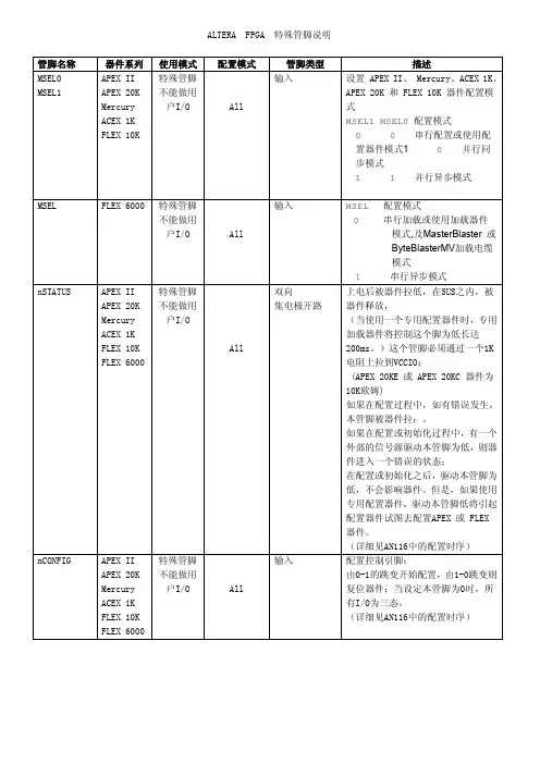
ALTERA FPGA 特殊管脚说明
- 格式:pdf
- 大小:165.61 KB
- 文档页数:4
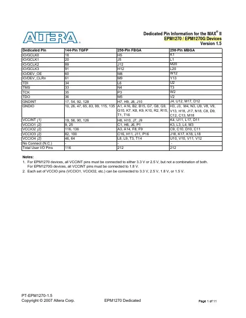
Dedicated Pin 144-Pin TQFP 256-Pin FBGA 256-Pin MBGA IO/GCLK018H5K1IO/GCLK120J5L1IO/GCLK289J12M20IO/GCLK391H12L20IO/DEV_OE60M8W12IO/DEV_CLRn61M9Y13TDI34L6U2TMS33N4T3TCK35P3W2TDO36M5V2GNDINT17, 54, 92, 128H7, H9, J8, J10J4, U12, M17, D12GNDIO 10, 26, 47, 65, 83, 99, 115, 135A1, A16, B2, B15, G7, G8, G9,G10, K7, K8, K9, K10, R2, R15,T1, T16H3, J3, M4, N3, U9, V8, V9, V13, H18, J17, N18, C8, D9, C12, C13, M18VCCINT (1)19, 56, 90, 126H8, H10, J7, J9K4, U11, L17, D11VCCIO1 (2)9, 25C1, H6, J6, P1K3, L3, L4, M3VCCIO2 (2)116, 136A3, A14, F8, F9C9, C10, D10, C11VCCIO3 (2) 82, 100 C16, H11, J11, P16J18, K17, K18, L18VCCIO4 (2) 46, 64 L8, L9, T3, T14U10, V10, V11, V12No Connect (N.C.)---Total User I/O Pins 116212212Notes:1. For EPM1270 devices, all VCCINT pins must be connected to either 3.3 V or2.5 V, but not a combination of both. For EPM1270G devices, all VCCINT pins must be connected to 1.8 V.2. Each set of VCCIO pins (VCCIO1, VCCIO2, etc.) can be connected to3.3 V, 2.5 V, 1.8 V, or 1.5 V.Dedicated Pin Information for the MAX ®IIEPM1270 / EPM1270G DevicesVersion 1.5Bank Number Pad Number Orientation Pin/Pad Function Optional Function(s)144-Pin TQFP 256-Pin FBGA 256-Pin MBGAB10VCCIO1B11GNDIOB12IO D3E3B13IO C2C2B14IO 1E3H2B15IO 2C3D3B16IO E4C3B17IO 3D2D2B18IO E5C4B19IO 4D1C1B110IO F3F3B111IO 5E2B1B112VCCIO1B113GNDIOB114IO 6F4D4B115IO E1D1B116IO F5H4B117IO F2F2B118IO 7F6G4B119IO 8F1E1B120IO G3J2B121IO G2G2B122IO G4E4B123IO G1E2B124VCCIO1B125GNDIOB126IO 11G5G3B127IO 12H2G1B128IO 13G6F4B129IO 14H1H1B130IO 15H3F1B131IO 16J1J132GNDINTB133IO GCLK018H5K134VCCINTB135IO GCLK120J5L1B136IO 21H4K2B137IO 22J2M1B138IO 23J4L2B139IO 24K1N1B140VCCIO1B141GNDIOB142IO J3M2B143IO 27K2P1B144IO K6N4B145IO L1R1B146IO 28K5P4B147IO 29L2P2B148IO K4R4B149IO M1T1B150IO K3N2B151IO 30M2U1B152IO L5P3B153IO M3R2B154VCCIO1B155GNDIOB156IO 31L4R3EPM1270 / EPM1270G DevicesVersion 1.5Bank Number Pad Number Orientation Pin/Pad Function Optional Function(s)144-Pin TQFP 256-Pin FBGA 256-Pin MBGAEPM1270 / EPM1270G DevicesVersion 1.5B157IO N1V1B158IO L3T4B159IO 32N2W1B160IO M4V3B161IO N3T2B162TMS 33N4T3B163TDI 34L6U2B164TCK 35P3W2B165TDO 36M5V2B166IO P2U3B167VCCIO1B168GNDIOB169N.C. (1)B470VCCIO4B471GNDIOB472IO P4V4B473IO 37R1W3B474IO 38P5V5B475IO T2Y1B476IO N5W5B477IO 39R3W4B478IO P6U4B479GNDIOB480VCCIO4B481IO 40R4Y2B482IO 41N6U5B483IO T4W6B484IO M6U6B485IO R5Y3B486IO 42P7V6B487IO 43T5Y4B488IO 44N7V7B489IO R6W7B490IO M7U7B491IO T6Y5B492IO L7U8B493IO 45R7Y6B494VCCIO4B495GNDIOB496IO 48P8W8B497IO 49T7Y7B498IO 50N8W9B499IO 51R8Y8B4100IO 52N9W10B4101IO 53T8Y9102GNDINTB4103IO 55T9Y10104VCCINTB4105IO 57R9Y11B4106IO 58P9W11B4107IO 59T10Y12B4108IO DEV_OE 60M8W12B4109IO DEV_CLRn 61M9Y13B4110IO 62L10U16B4111IO 63R10Y14B4112VCCIO4B4113GNDIOBank Number Pad Number Orientation Pin/Pad Function Optional Function(s)144-Pin TQFP 256-Pin FBGA 256-Pin MBGAEPM1270 / EPM1270G DevicesVersion 1.5B4114IO M10U13B4115IO T11Y15B4116IO 66N10V15B4117IO 67R11Y16B4118IO P10W14B4119IO T12W15B4120IO 68M11U14B4121IO R12W16B4122IO N11V14B4123IO 69T13Y17B4124IO P11W13B4125IO R13Y18B4126VCCIO4B4127GNDIOB4128IO 70M12U15B4129IO R14Y19B4130IO N12V16B4131IO 71T15W17B4132IO P12V17B4133IO R16W18B4134IO 72P13V18B4135VCCIO4B4136GNDIOB3137VCCIO3B3138GNDIOB3139IO P14W19B3140IO N13U18B3141IO P15V19B3142IO 73M14T18B3143IO 74N14U19B3144IO 75M13R18B3145IO N15Y20B3146IO 76L14W20B3147IO N16T19B3148VCCIO3B3149GNDIOB3150IO L13U17B3151IO 77M15V20B3152IO L12P17B3153IO M16R19B3154IO L11T17B3155IO 78L15U20B3156IO 79K14N19B3157IO 80L16T20B3158IO K13R17B3159IO K15P19B3160IO 81K12P18B3161IO K16R20B3162VCCIO3B3163GNDIOB3164IO 84K11N17B3165IO 85J15P20B3166IO 86J14M19B3167IO 87J16N20B3168IO 88J13L19B3169IO GCLK289J12M20170VCCINTBank Number Pad Number Orientation Pin/Pad Function Optional Function(s)144-Pin TQFP 256-Pin FBGA 256-Pin MBGAEPM1270 / EPM1270G DevicesVersion 1.5B3171IO GCLK391H12L20172GNDINTB3173IO 93H16K20B3174IO 94H13K19B3175IO 95H15J20B3176IO 96H14J19B3177IO 97G16H20B3178IO 98G12G18B3179GNDIOB3180VCCIO3B3181IO 101G15G20B3182IO G11H17B3183IO F16G19B3184IO G13F17B3185IO 102F15F20B3186IO 103G14E17B3187IO E16E20B3188IO F11G17B3189IO E15F19B3190IO 104F12D17B3191IO 105D16D20B3192IO F13C18B3193GNDIOB3194VCCIO3B3195IO 106D15C20B3196IO F14H19B3197IO 107D14B20B3198IO E12F18B3199IO 108C15E19B3200IO E13E18B3201IO C14D19B3202IO E14D18B3203IO D13C19B3204N.C. (1)B3205VCCIO3B3206GNDIOB2207VCCIO2B2208GNDIOB2209IO C13C16B2210IO 109B16A20B2211IO 110C12B16B2212IO 111A15B17B2213IO D12C15B2214GNDIOB2215VCCIO2B2216IO B14A19B2217IO C11B18B2218IO B13A18B2219IO 112D11B19B2220IO A13A17B2221IO E11D15B2222IO 113B12B15B2223IO C10C17B2224IO A12B14B2225IO 114D10C14B2226IO B11A16B2227IO E10D16Bank Number Pad Number Orientation Pin/Pad Function Optional Function(s)144-Pin TQFP 256-Pin FBGA 256-Pin MBGAEPM1270 / EPM1270G DevicesVersion 1.5B2228GNDIOB2229VCCIO2B2230IO 117A11B13B2231IO 118F10D13B2232IO 119B10A15B2233IO 120C9B12B2234IO 121A10A14B2235IO 122D9D14B2236IO 123B9A13B2237IO 124E9B11B2238IO 125A9A12239VCCINTB2240IO 127A8A11241GNDINTB2242IO 129B8A10B2243IO 130E8B10B2244IO 131A7A9B2245IO 132D8D8B2246IO 133B7A8B2247IO 134C8B9B2248GNDIOB2249VCCIO2B2250IO A6A7B2251IO F7D7B2252IO B6B7B2253IO 137E7C6B2254IO 138A5A6B2255IO 139D7C7B2256IO B5A5B2257IO C7B8B2258IO 140A4A4B2259IO 141E6D6B2260IO B4B6B2261IO D6D5B2262IO 142C4A3B2263IO C6B2B2264GNDIOB2265VCCIO2B2266IO B3A2B2267IO C5B3B2268IO 143A2B5B2269IO D5C5B2270IO B1A1B2271IO 144D4B4B2272VCCIO2B2273GNDIONote:1. No ConnectPin NamePin Type Pin DescriptionVCCIO[1..4]Power I/O supply voltage pins for banks 1 through 4. Each VCCIO bank supports a differentvoltage level with the VCCIO pins providing power for the input and output buffers withinthat particular I/O bank. Each VCCIO bank can be powered with either 3.3 V, 2.5 V, 1.8 V,or 1.5 V.GNDIO Ground Ground pins for all the I/O banks.VCCINT Power Voltage supply pins for the device.GNDINT Ground Ground pins for the internal supply.NC No Connect Do not drive signals into these pins.DEV_CLRn I/O Dual-purpose pin that can override all clears on all device registers. All registers arecleared when the pin is driven low and all registers behave as defined in the design whenthis pin is driven high. If not used for its dual-purpose function, this pin is a regular I/O.DEV_OE I/O Dual-purpose pin that can override all tri-states on the device. All output pins are tri-statedwhen the pin is driven low and all output pins behave as defined in the design when thispin is driven high. If not used for its dual-purpose function, this pin is a regular I/O.TCK Input Dedicated JTAG input pin.TDI Input Dedicated JTAG input pin.TMS Input Dedicated JTAG input pin.TDO Output Dedicated JTAG output pin.GCLK [0..3]I/ODual-purpose clock pins that connect to the global clock network. If not used forits dual-purpose function, this pin is a regular I/O.Programming and JTAG pinsClock PinsPin Definitions for the MAX ®IIEPM1270 / EPM1270G DevicesVersion 1.5Supply and Reference pinsFigure 1. MAX II EPM1270 / EPM1270G T144 Device Top View Package Diagram and Bank Information Package Diagram and Bank Information for the MAX ® IIEPM1270 / EPM1270G DevicesVersion 1.5Figure 2. MAX II EPM1270 / EPM1270G F256 Device Top View Package Diagram and Bank Information Package Diagram and Bank Information for the MAX ® IIEPM1270 / EPM1270G DevicesVersion 1.5Figure 3. MAX II EPM1270 / EPM1270G M256 Device Top View Package Diagram and Bank Information Package Diagram and Bank Information for the MAX ® II EPM1270 / EPM1270G DevicesVersion 1.5DateVersion Changes Made Sep-071.5Added support for M256 package in the EPM1270G device May-071.4Changed the VCCIO2 and VCCIO4 pins for EPM1270 (256-Pin MBGA package) to match Quartus II pin-out Apr-061.3Added M256 package Jan-051.2Added MAX IIG device naming to titles, notes, and figures Jul-041.1Added package diagram and bank information figures for each package May-04 1.0Initial release Revision History for the MAX ® II EPM1270 / EPM1270G DevicesVersion 1.5PT-EPM1270-1.5Copyright © 2007 Altera Corp.Revision History Page 11 of 11。
fpga配特殊引脚的含义(FPGA with the meaning of a special pin)FPGA with the meaning of a special pin1.I/O, ASDOIn AS mode, it is dedicated output pin, and can be used as I/O pin in PS and JTAG mode. In AS mode, this pin is the CII pin that sends the control signal to the serial configuration chip. Also used to read configuration data from the configuration chip. In AS mode, the ASDO has an internal pullup resistor, which has been in effect until the configuration is completed, and the pin becomes a three state input pin. The ASDO pin is connected directly to the ASDI pin (fifth feet) of the configuration chip.2.I/O, nCSOIn AS mode, it is a dedicated output pin that can be used as the I/O pin in PS and JTAG mode. In AS mode, this pin is used by the CII to send the enable pins to the outside serial configuration chip. In AS mode, the ASDO has an internal pullup resistor that has been in effect. This pin is active low. The /CS pin (first feet) is directly connected to the configuration chip.3.I/O, CRC_ERRORWhen the error detection CRC circuit is selected, this foot is used as the CRC_ERROR pin, and if not used by default, it is used as I/O. Note, however, that this pin does not support open drain and reverse. When it is used as CRC_ERROR, the high leveloutput indicates a CRC checksum error (when an individual bit of the SRAM is configured). CRC circuit support can be added to the setting. This foot is usually used with the nCONFIG foot. That is, if the configuration process is wrong, reconfigure it4.I/O, CLKUSRWhen the Enable User-supplled start-up clock (CLKUSR) option is opened in the software, this pin can only be used as an initialization clock input for the user. In all configuration data have been received, CONF_DONE pin will become a high level, the CII device 299 clock cycles are needed to initialize the I/O register, FPGA and so on, there are two ways, one is using the internal oscillator (10MHz), another is from CLKUSR in the clock (maximum not more than 100MHz). This feature can delay the time FPGA starts working and can be used in special applications that require synchronization with other devices.5.I/O, VREFUsed to provide a reference level for certain differential standards. If not used, you can use it as a I/O.6. DATA0Dedicated input pin. In AS mode, the configuration process is: CII sets the nCSO low, and the configured chip is enabled. CII then cooperates with DCLK and ASDO to send commands and read addresses to the configuration chip. Configure the chip and then send the data to the CII via the DATA pin. The DATA foot is attached to the CII's DATA0 foot. After all configurationdata is received by the CII, the CONF_DONE pin is released (that is, the CONF_DONE pin is not forced low) and the CONF_DONE pin is open drain (Open-Drain). At this point, the 10K will turn on a high level because the CONF_DONE will pick up a resistor on the outside. At the same time, the CII stops the DCLK signal. After the CONF_DONE becomes high (when it becomes equivalent to an input pin), the initialization process begins. So, CONF_DONE must have a 10K resistor on the outside of the foot to ensure that the initialization process starts correctly. DATA0, DCLK, NCSO, and ASDO have weak pullup resistors on their feet, and they are always valid. Upon completion of the configuration, these pins are turned into an input three state, and the level is set to a high level by an internal pullup resistor. In AS mode, the DATA0 receives the DATA (second pin) of the configuration chip.7. DCLKPS mode is input, AS mode is output. In PS mode, the DCLK is a clock input pin that is the clock that the external device sends the configuration data to the FPGA. Data is placed on the rising edge of the DCLK to data in AS mode, and the DCLK pin is a clock output pin that is configured to provide a clock. Connect directly to the DCLK pin of the configuration chip (sixth feet). No matter what configuration mode, after the configuration is completed, this foot will become three states. If an external configuration device is attached, the configuration device will set the DCLK pin to low level. If you are using the master chip, you can either set the DCLK high or you can lower the DCLK. When the configuration is complete, triggering this pin does not affect the configured FPGA. Thispin has an input Buffer that supports the hysteresis function of the Schmidt flip-flop.8. nCEDedicated input pin. This pin is an active low chip enable signal. The nCE pin is configured to enable the foot. In configuration, initialization, and user mode, the nCE pin must be set low. In the configuration of multiple devices, the nCE pin of the first device is set low, and its nCEO is connected to the nCE pin of the next device, forming a chain. The nCE pin also requires a low nCE foot in the JTAG programming mode.This pin has an input Buffer that supports the hysteresis function of the Schmidt flip-flop.9. nCONFIGDedicated input pins. This pin is a configuration control input pin. If this foot is low in user mode, the FPGA loses its configuration data and goes into a reset state and sets all the I/O feet into three states. The process of changing nCONFIG from low level to high level will initialize the reconfiguration process. If the configuration scheme uses an enhanced configuration device or EPC2, the user can connect the nCONFIG pin directly to the VCC or to the nINIT_CONF pin of the configuration chip. This pin has an input Buffer that supports the hysteresis function of the Schmidt flip-flop. In fact, in user mode, the nCONFIG signal is used to initialize the reconfiguration. When the nCONFIG foot is low, the initialization process begins. When the nCONFIG pin is low, theCII is reset and goes into the reset state. The nSTATUS and CONF_DONE pins are set low and all the I/O pins are in the three state. The nCONFIG signal must remain at least 2us. When nCONFIG returns to the high level state, the nSTATUS is released again. The reconfiguration starts. In actual application, the nCONFIG pin can be connected with a pull-up resistor of 10K to 3.3V.10. DEV_OEI/O pin or global I/O enable pin. In the Quartus II software can enable the DEV_OE option (Enable Device-wideoutput Enable), if can make this a function, this pin can be enabled when the global I/O feet, this foot function is, if it is set low, all I/O into three states.11. INIT_DONEI/O pin or drain open output pin. When this foot is enabled, the foot jumps from low to high, indicating that the FPGA has entered the user mode. If the INIT_DONE output pin is enabled, this pin cannot be used as user I/O after configuration is complete. Inside the QuartusII, this pin can be enabled by enabling the Enable INIT_DONE output option.12. nCEOI/O pin or output pin. When the configuration is complete, this pin outputs low level. In the configuration of multiple devices, this pin will connect to the next device's nCE pin. This time, it also needs a 10K pull-up resistor outside to Vccio. The configuration process of multiple devices, finally a nCEOdevice can float. If you want to use this pin as an available I/O, you need to set it up inside the software. In addition, even if the I/O, but also after the completion of the configuration.13. nSTATUSThis is a dedicated configuration status pin. Two way foot, when it is the output pin, is open drain. After power on, the FPGA immediately sets the nSTATUS foot low and releases it after power on reset (POR) and sets it high. As a status output pin, if any error occurs during configuration, the nSTATUS pin is lowered. As the status input pin, during the configuration or initialization, the external control chip can pull this pin down, and FPGA will enter the wrong state at this time. This foot can not be used as an ordinary I/O foot. The nSTATUS pin must be pulled up by a 10K ohm resistor.14. CONF_DONEThis is a dedicated configuration status pin. Two way foot, when it is the output pin, is open drain. When it is used as a status output pin, it is set low before and during configuration. Once the configuration data is received and no errors are made, the CONF_DONE will be released at the start of the initialization cycle. When used as a status input pin, after all data has been received, it should be set to a high level. After that, the device starts initialization and goes into user mode. It should not be used as a regular I/O. The outside of the foot must also be connected with a 10K ohm resistor.15. MSEL[1:0]These pins should be connected to zero or power, indicating high or low level. 00 with AS mode, 10 PS mode, AS mode is 01 FAST. If in JTAG mode, it with their 00 JTAG mode and the MSEL has nothing to do with JTAG mode, MSEL will be ignored, but because they can not float, so suggest that it be received.16 DEV_CLRnI/O or global clear input. In QuartusII, if you choose the Enable Device-Wide Reset (DEV_CLRn) this function. This pin is the global reset. When this pin is low, all registers are cleared. This pin does not affect the JTAG's boundary scan or programming operations.Application of FPGA configuration pinFor FPGA applications, you need to know the following points.The nCONFIG, nSTATUS, and CONF_DONE require the pull-up resistor of the 10K, and the nCE requires a 10K pull-down resistor;NCONFIG for configuration control, the dedicated input pin sets the low FPGA to lose data;The nSTATUS is a dedicated bidirectional pin for the FPGA. 0 indicates that the FPGA is in a busy state and is released at 1 after the pull-up, and the FPGA begins to be in configuration.CONF_DONE dedicated configuration, two-way feet, FPGA configuration is 0, after the configuration is released, the role of the external pull-up is 1. NCE configuration enables dedicated input pins. In configuration, initialization, and user mode, the nCE pin must be set low.MSEL configure pin for mode;TDI, TMS, 10K pull-up resistor, TCK, 10K pull-down resistor, for JTAG;ASDO, nCSO, DCLK and DATA0 are used for the communication between FPGA and configuration chip, and there is no pullup on the inside, and no external resistance is needed.The clock pin can only be input and cannot be output.6 、 pull / pull resistance:1) ensure that the initial values of the circuit. For example, TCK signal using a pull-down resistor. Why the pull-down resistor instead of the pull-up resistor? Because pull-down resistor makes the initial value of the TCK signal is 0, because it is a clock signal, can guarantee the clock signal in the initial value after the first rise along the edge, and the JTAG control of resistance it is on the rising edge of TCK to write configuration data within the FPGA.2) here / pull-down resistor only belongs to the recommended value, determine the value is not, the purpose is to ensure the quality of the signal. The resistance as an example, if thepull-up resistor is above 10K, the pin has an equivalent capacitance to ground, because T=RC, C by the device process, the greater the resistance, charge and discharge the longer the time, the rising edge of the slower signal, the slope is small. The rise time if more than JTAG control circuit requirements to write data within the FPGA may be wrong. So, if the pull-up resistor smaller? Will rise time smaller? Yes. Resistance decreases, rise time small, the slope becomes larger, but also brought a serious problem, if the resistance is small to a certain extent, the signal will be at the rising edge of the emergence of the red signal ringing phenomenon, will seriously. If the resistance is too small, the intrusion tolerance over current devices IO, JTAG control circuit Will burn out. So, what is the resistance to meet the general requirements of PCB using 4.7K. in general?3) to ensure the driving ability of signal. As mentioned earlier, the resistance is small, the signal slope is small, and the driving force of signals is stronger. The more resistance signal slope is bigger, and the driving force of signals is weak. This point in the JTAG daisy chain circuit and its important。
ALTERA FPGA EP2C5Q 开发板用户手册上海亿家网络有限公司版权所有 © 上海亿家网络有限公司 2013。
保留一切权利。
非经上海亿家网络有限公司书面同意,任何单位和个人不得擅自摘抄、复制本手册内容的部分或全部,并不得以任何形式传播。
本手册中描述的产品中,可能包含上海亿家网络有限公司及其可能存在的许可人享有版权的软件,除非获得相关权利人的许可,否则,任何人不能以任何形式对前述软件进行复制、分发、修改、摘录、反编译、反汇编、解密、反向工程、转让、分许可以及其他侵犯软件版权的行为。
本手册描述了ALTERA FPGA EP2C5Q开发板的硬件资源、安装、使用和设计原理,用以指导开发板使用。
本手册对应开发板的主要用户为高校学生、电子爱好者、科研单位、企事业单位的开发设计人员,适合于产品原型的快速开发、学生参加各种电子设计大赛、学习FPGA技术入门、课程设计及毕业设计等,亦可用于系统设计前期快速评估,特别适合于FPGA、NIOSII、SOPC 快速入门和产品开发及验证。
1 安全警告和注意事项 (5)2开发板主要器件及硬件资源 (7)2.1 主要器件 (7)2.2 硬件资源 (7)2.3 PCB和尺寸 (9)3 开发板的安装和使用 (10)3.1 开发板安装 (10)3.2 开发板的使用 (11)4开发板设计详细说明 (17)4.1 电源电路 (17)4.2 时钟电路 (17)4.3 复位电路 (18)4.4 JTAG接口电路 (18)4.5 AS接口电路 (19)4.6 LED电路 (19)4.7 存储器SDRAM电路 (19)4.8外部扩展IO (21)5技术支持与保修 (23)5.1关于技术支持 (23)5.2 关于产品保修 (23)附录常见问题解答 (24)1安全警告和注意事项为正确、安全地使用本开发板,请您在使用前仔细阅读本安全警告和注意事项,并在使用时严格遵循。
说明如无特别说明,本节描述的“开发板”包含开发板本身及其配件。

F PG A的配置引脚说明FPGA是基于SRAM编程的,编程信息在系统掉电时会丢失,每次上电时,都需要从器件外部的FLASH或EEPROM中存储的编程数据重现写入内部的SRAM中。
FPGA在线加载需要有CPU的帮助,并且在加载前CPU已经启动并工作。
FPGA的加载模式主要有以下几种:1).PS模式(Passive Serial Configuration Mode),即被动串行加载模式。
PS模式适合于逻辑规模小,对加载速度要求不高的FPGA加载场合。
在此模式下,加载所需的配置时钟信号CCLK由FPGA外部时钟源或外部控制信号提供。
另外,PS加载模式需要外部微控制器的支持。
2).AS模式(Active Serial Configuration Mode),即主动串行加载模式。
在AS模式下,FPGA主动从外部存储设备中读取逻辑信息来为自己进行配置,此模式的配置时钟信号CCLK由FPGA内部提供。
3).PP模式(Passive Parallel Configuration Mode),即被动并行加载模式。
此模式适合于逻辑规模较大,对加载速度要求较高的FPGA加载场合。
PP 模式下,外部设备通过8bit并行数据线对FPGA进行逻辑加载,CCLK信号由外部提供。
4).BS模式(Boundary Scan Configuration Mode),即边界扫描加载模式。
也就是我们通常所说的JTAG加载模式。
所有的FPGA芯片都有三个或四个加载模式配置管脚,通过配置MESL[0..3]来选取不同的加载模式。
首先来介绍下PS加载模式,各个厂商FPGA产品的PS加载端口定义存在一些差异,下面就对目前主流的三个FPGA厂商Altera, Xilinx,Lattice的PS加载方式进行一一介绍。
Altera公司的FPGA产品PS加载接口如下图所示。
1).CONFIG_DONE:加载完成指示输出信号,I/O接口,高有效,实际使用中通过4.7K电阻上拉到VCC,使其默认状态为高电平,表示芯片已加载完毕,当FPGA正在加载时,会将其驱动为低电平。
XilinxFPGA引脚功能详细介绍注:技术交流用,希望对大家有所帮助。
IO_LXXY_# 用户IO引脚XX代表某个Bank内唯一的一对引脚,Y=[P|N]代表对上升沿还是下降沿敏感,#代表bank号2.IO_LXXY_ZZZ_# 多功能引脚ZZZ代表在用户IO的基本上添加一个或多个以下功能。
Dn:I/O(在readback期间),在selectMAP或者BPI模式下,D[15:0]配置为数据口。
在从SelectMAP读反馈期间,如果RDWR_B=1,则这些引脚变成输出口。
配置完成后,这些引脚又作为普通用户引脚。
D0_DIN_MISO_MISO1:I,在并口模式(SelectMAP/BPI)下,D0是数据的最低位,在Bit-serial模式下,DIN是信号数据的输入;在SPI模式下,MISO是主输入或者从输出;在SPI*2或者SPI*4模式下,MISO1是SPI总线的第二位。
D1_MISO2,D2_MISO3:I,在并口模式下,D1和D2是数据总线的低位;在SPI*4模式下,MISO2和MISO3是SPI总线的MSBs。
An:O,A[25:0]为BPI模式的地址位。
配置完成后,变为用户I/O 口。
AWAKE:O,电源保存挂起模式的状态输出引脚。
SUSPEND是一个专用引脚,AWAKE是一个多功能引脚。
除非SUSPEND模式被使能,AWAKE 被用作用户I/O。
MOSI_CSI_B_MISO0:I/O,在SPI模式下,主输出或者从输入;在SelectMAP模式下,CSI_B是一个低电平有效的片选信号;在SPI*2或者SPI*4的模式下,MISO0是SPI总线的第一位数据。
FCS_B:O,BPI flash 的片选信号。
FOE_B:O,BPI flash的输出使能信号FWE_B:O,BPI flash 的写使用信号LDC:O,BPI模式配置期间为低电平HDC:O,BPI模式配置期间为高电平CSO_B:O,在并口模式下,工具链片选信号。

1.下载口。
JTAG下载接口,对应下载的文件是SOF文件,速度快,JTAG 将程序直接下载到FPGA中,但是掉电程序丢失,平时学习推荐使用JTAG方式,最后固化程序的时候再通过AS方式将程序下载到配置芯片中即可;AS下载接口,对应下载的是POF文件,速度相对较慢,需要重新上电并且拔掉下载线,才能工作,操作相对麻烦,不推荐学习的时候使用。
2.FPGA引脚作用:(1)VCCINT:这些都是内部逻辑阵列电源电压引脚。
VCCINT还可以给输入缓冲区供电,用于LVPECL,LVDS(常规I / O和CLK引脚),差分HSTL,差分SSTL I/ O标准。
Connect all VCCINT pins to 1.2 V. Decoupling depends on the design decoupling requirementsof the specific board.所有VCCINT引脚连接至1.2 V,去耦依赖于设计脱钩的要求的具体电路板。
(2)VCCIO[1…8]: 这些I / O电源电压引脚银行1至8。
每个组可以支持不同的电压水平。
VCCIO供电到输出缓冲区,所有的I / O标准。
VCCIO供电输入缓冲区用于LVTTL,LVCMOS,1.5-V,1.8 V,2.5 V,3.3 V PCI,和3.3-V PCI-X,差分SSTL。
差分HSTL。
和LVDS lrecular我/ OL I / O标准。
验证VCCIO电压等级连接是与QuartusII软件的引脚连接一致。
去耦取决于设计去耦的具体要求的具体电路板。
(3)VREFB[1..8]N[0..3]: 为每个I / O组的输入参考电压。
这些引脚被用来作电压参考引脚。
如果没有被用,就作为普通的I/O引脚。
(4)VCCA PLL[1..4]: 模拟电源锁相环[1 ..4].将这些引脚连接到1.2 V,即使不使用PLL。
更好的,使用一个孤立的线性电源钳工性能。
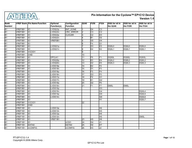
Pin NamePin Type (1st, 2nd, &3rd Function)Pin DescriptionVCCIO[1..4]Power These are I/O supply voltage pins for banks 1 through 4. Each bank can support a different voltage level. VCCIO supplies power to the output buffers for all I/O standards. VCCIO also supplies power to the input buffers used for the LVTTL, LVCMOS, 1.5-V, 1.8-V, 2.5-V, and 3.3-V PCI I/O standards.VCCINT Power These are internal logic array voltage supply pins. VCCINT also supplies power to the input buffers used for the LVDS, SSTL2, and SSTL3 I/O standards.GNDGroundDevice ground pins. All GND pins should be connected to the board GND plane.VREF[0..2]B[1..4]I/O, Input Input reference voltage for banks 1-4. If a bank uses a voltage-referenced I/O standard, then these pins are used as the voltage-reference pins for the bank. If voltage reference I/O standards are not used in the bank, the VREF pins are available as user I/O pins.VCCA_PLL[1..2]Power Analog power for PLLs[1..2]. The designer must connect this pin to 1.5 V, even if the PLL is not used.GNDA_PLL[1..2]Ground Analog ground for PLLs[1..2]. The designer can connect this pin to the GND plane on the board.GNDG_PLL[1..2]Ground Guard ring ground for PLLs[1..2]. The designer can connect this pin to the GND plane on the board.NCNo Connect No connect pins should not be connected on the board. They should be left floating.CONF_DONE Bidirectional (open-drain)This is a dedicated configuration status pin; it is not available as a user I/O pin.nSTATUS Bidirectional (open-drain)This is a dedicated configuration status pin; it is not available as a user I/O pin.nCONFIGInputDedicated configuration control input. A low transition resets the target device; a low-to-high transition begins configuration. All I/O pins tri-state when nCONFIG is driven low.DCLK Input (PS mode), Output (AS mode)In passive serial configuration mode, DCLK is a clock input used to clock configuration data from an external source into the Cyclone device. In active serial configuration mode, DCLK is a clock outputfrom the Cyclone device (the Cyclone device acts as master in this mode). This is a dedicated pinused for configuration.DATA0InputDedicated configuration data input pin.nCE Input Active-low chip enable. Dedicated chip enable input used to detect which device is active in a chain of devices. When nCE is low, the device is enabled. When nCE is high, the device is disabled.nCEOOutputOutput that drives low when device configuration is complete. During multi-device configuration, this pin feeds a subsequent device’s nCE pin.ASDO I/O, OutputActive serial data output from the Cyclone device. This output pin is utilized during active serial configuration mode. The Cyclone device controls configuration and drives address and control information out on ASDO. In passive serial configuration, this pin is available as a user I/O pin.nCSO I/O, OutputChip select output that enables/disables a serial configuration device. This output is utilized during active serial configuration mode. The Cyclone device controls configuration and enables the serial configuration device by driving nCSO low. In passive serial configuration, this pin is available as a user I/O pin.CRC_ERRORI/O, OutputActive high signal that indicates that the error detection circuit has detected errors in the configuration SRAM bits. This pin is optional and is used when the CRC error detection circuit is enabled.INIT_DONE I/O, Output (open-drain)This is a dual-purpose pin and can be used as an I/O pin when not enabled as INIT_DONE. When enabled, the pin indicates when the device has entered user mode. This pin can be used as a user I/Opin after configuration.CLKUSRI/O, InputOptional user-supplied clock input. Synchronizes the initialization of one or more devices. This pin can be used as a user I/O pin after configuration.DEV_CLRn I/O, InputDual-purpose pin that can override all clears on all device registers. When this pin is driven low, all registers are cleared; when this pin is driven high, all registers behave as defined in the design.DEV_OE I/O, Input Dual-purpose pin that can override all tri-states on the device. When this pin is driven low, all I/O pins are tri-stated; when this pin is driven high, all I/O pins behave as defined in the design.MSEL[1..0]Input Dedicated mode select control pins that set the configuration mode for the device.TMS Input This is a dedicated JTAG input pin.TDI Input This is a dedicated JTAG input pin.TCK Input This is a dedicated JTAG input pin.TDO OutputThis is a dedicated JTAG output pin.CLK0Input, LVDS Input Dedicated global clock input. The dual-function of CLK0 is LVDSCLK1p, which is used for differential input to PLL1.CLK1Input, LVDS Input Dedicated global clock input. The dual-function of CLK1 is LVDSCLK1n, which is used for differential input to PLL1.CLK2Input, LVDS Input Dedicated global clock input. The dual-function of CLK2 is LVDSCLK2p, which is used for differential input to PLL2.CLK3Input, LVDS InputDedicated global clock input. The dual-function of CLK3 is LVDSCLK2n, which is used for differential input to PLL2.Configuration and JTAG Pins Pin Information for the Cyclone™ EP1C12 DeviceVersion 1.4Supply and Reference PinsClock and PLL PinsPT-EP1C12-1.4Copyright © 2006 Altera Corp.Pin DefinitionsPage 12 of 15Pin NamePin Type (1st, 2nd, & 3rd Function)Pin DescriptionPin Information for the Cyclone™ EP1C12 DeviceVersion 1.4DPCLK[7..0]I/O Dual-purpose clock pins that can connect to the global clock network. These pins can be used forhigh fan-out control signals, such as clocks, clears, IRDY, TRDY, or DQS signals. These pins are also available as user I/O pins.PLL1_OUTp I/O, Output External clock output from PLL 1. This pin can be used with differential or single ended I/O standards. If clock output from PLL1 is not used, this pin is available as a user I/O pin.PLL1_OUTn I/O, Output Negative terminal for external clock output from PLL1. If the clock output is single ended, this pin is available as a user I/O pin.PLL2_OUTp I/O, Output External clock output from PLL 2. This pin can be used with differential or single ended I/O standards. If clock output from PLL2 is not used, this pin is available as a user I/O pin.PLL2_OUTnI/O, OutputNegative terminal for external clock output from PLL2. If the clock output is single ended, this pin is available as a user I/O pin.LVDS[0..102]p I/O, LVDS RX or TXDual-purpose LVDS I/O channels 0 to 102. These channels can be used for receiving or transmitting LVDS compatible signals. Pins with a "p" suffix carry the positive signal for the differential channel. If not used for LVDS interfacing, these pins are available as user I/O pins.LVDS[0..102]n I/O, LVDS RX or TX Dual-purpose LVDS I/O channels 0 to 102. These channels can be used for receiving or transmitting LVDS compatible signals. Pins with an "n" suffix carry the negative signal for the differential channel. If not used for LVDS interfacing, these pins are available as user I/O pins.LVDSCLK1p Input, LVDS Input Dual-purpose LVDS clock input to PLL1. If differential input to PLL1 is not required, this pin is available as the CLK0 input pin.LVDSCLK1n Input, LVDS Input Dual-purpose LVDS clock input to PLL1. If differential input to PLL1 is not required, this pin is available as the CLK1 input pin.LVDSCLK2p Input, LVDS Input Dual-purpose LVDS clock input to PLL2. If differential input to PLL2 is not required, this pin is available as the CLK2 input pin.LVDSCLK2nInput, LVDS InputDual-purpose LVDS clock input to PLL2. If differential input to PLL2 is not required, this pin is available as the CLK3 input pin.DQS[0..1][L,R,T,B]I/O Optional data strobe signal for use in external memory interfacing. These pins also function as DPCLK pins; therefore, the DQS signals can connect to the global clock network. A programmable delay chain is used to shift the DQS signals by 90 or 72 degrees.DQ[0..7][L,R,T,B]I/O Optional data signal for use in external memory interfacing.DM[0..1][L,R,T,B]I/OOptional data mask output signal for use in external memory interfacing.Dual-Purpose LVDS & External Memory Interface PinsPT-EP1C12-1.4Copyright © 2006 Altera Corp.Pin DefinitionsPage 13 of 15Pin Information for the Cyclone™ EP1C12 Device, ver 1.4VREF2B2VREF1B2VREF0B2B2V R E F 0B 1B 1B 3V R E F 0B 3V R E F 1B 1V R E F 1B 3PLL1PLL2V R E B 2B 1V R E B 2B 3B4VREF2B4VREF1B4VREF0B4Notes:1.This is a top view of the silicon die.2.This is a pictoral representation only to get an idea of placement on the device. Refer to the pin-list andthe Quartus II for exact locations.PT-EP1C12-1.4Copyright © 2006 Altera Corp.Bank & PLL DiagramPage 14 of 15Pin Information for the Cyclone™ EP1C12 DeviceVersion 1.4Version NumberDate Changes Made1.43/6/2006Added CRC_ERROR pin in Pin List and Pin DefinitionsPT-EP1C12-1.4Copyright © 2006 Altera Corp.Revision HistoryPage 15 of 15。
用户I/O:不用解释了。
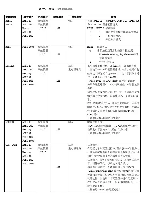
配置管脚:MSEL[1:0] 用于选择配置模式,比如AS、PS等。
DATA0 FPGA串行数据输入,连接到配置器件的串行数据输出管脚。
DCLK FPGA串行时钟输出,为配置器件提供串行时钟。
nCSO(I/O)FPGA片选信号输出,连接到配置器件的nCS管脚。
ASDO(I/O)FPGA串行数据输出,连接到配置器件的ASDI管脚。
nCEO 下载链期间始能输出。
在一条下载链中,当第一个器件配置完成后,此信号将始能下一个器件开始进行配置。
下载链上最后一个器件的nCEO悬空。
nCE 下载链器件始能输入,连接到上一个器件的nCEO,下载链的最后一个器件nCE接地。
nCNFIG 用户模式配置起始信号。
nSTATUS 配置状态信号。
CONF_DONE 配置结束信号。
电源管脚:VCCINT 内核电压。
130nm为1.5V,90nm为1.2VVCCIO 端口电压。
一般为3.3V,还可以支持多种电压,5V、1.8V、1.5VVREF 参考电压GND 信号地时钟管脚:VCC_PLL PLL管脚电压,直接连VCCIOVCCA_PLL PLL模拟电压,截止通过滤波器接到VCCINT上GNDA_PLL PLL模拟地GNDD_PLL PLL数字地CLK[n] PLL时钟输入PLL[n]_OUT PLL时钟输出特殊管脚:VCCPD 用于寻则驱动VCCSEL 用于控制配置管脚和PLL相关的输入缓冲电压PROSEL 上电复位选项NIOPULLUP 用于控制配置时所使用的用户I/O的内部上拉电阻是否工作TEMPDIODEN 用于关联温度敏感二极管******************************************************************************** ****************************************************1/1.I/O, ASDO在AS 模式下是专用输出脚,在PS 和JTAG 模式下可以当I/O 脚来用。
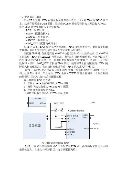
一、被动串行(PS)在做PS配置时,FPGA配置数据从储存器中读出,写入到FPGA的DATA0接口上。
这些存储器是FLASH器件。
数据由DCLK时钟信号管脚的上升沿打入FPGA,每个DCLK时钟周期输入1比特数据。
·DCLK(配置时钟);·DATA0(配置数据);·nCONFIG(配置命令);·nSTATUS(状态信号);·CONF_DONE(配置完成指示)。
在PS方式下,FPGA处于完全被动地位。
FPGA接收配置时钟、配置命令和配置数据,给出配置的状态信号以及配置完成指示信号等。
在配置FPGA时,首先需要将nCONFIG拉低(至少40us),然后拉高。
当nCONFIG 被拉高后,FPGA的nSTATUS也将变高,表示这时已经开始配置,外部电路旧可以用DCLK的时钟上升沿一位一位地将配置数据写入到FPGA中。
当最后一个比特数据写入以后,CONF_DONE管脚被FPGA释放,被外部的上拉电阻拉高,FPGA随即进入初始化状态。
在完成初始化过程后,FPGA正式进入用户模式。
【注】:有的配置芯片没有nINIT_CONF管脚,只需将FPGA的nCONFIG信号弱上拉到Vcc即可。
在上电后,FPGA会在nCONFIG管脚上检测到一个从低到高的跳变沿,因此可以自动启动配置过程。
有三种配置FPGA的方法:1、使用Altera的配置芯片与FPGA相连;2、使用下载电缆通过FPGA的PS口配置;3、使用微处理器配置FPGA。
下图是使用微处理器配置FPGA的示意图:PS:用微处理器配置FPGA【注】:如果外部器件将.rbf文件配置到FPGA中,必须确保配置文件中的最低位先入。
如果比特顺序错误,将导致配置失败。
C代码实现:。
FPGA是基于SRAM编程的,编程信息在系统掉电时会丢失,每次上电时,都需要从器件外部的FLASH或EEPROM中存储的编程数据重现写入内部的SRAM中。
FPGA在线加载需要有CPU的帮助,并且在加载前CPU已经启动并工作。
FPGA的加载模式主要有以下几种:1).PS模式(Passive Serial Configuration Mode),即被动串行加载模式。
PS模式适合于逻辑规模小,对加载速度要求不高的FPGA加载场合。
在此模式下,加载所需的配置时钟信号CCLK由FPGA外部时钟源或外部控制信号提供。
另外,PS加载模式需要外部微控制器的支持。
2).AS模式(Active Serial Configuration Mode),即主动串行加载模式。
在AS模式下,FPGA主动从外部存储设备中读取逻辑信息来为自己进行配置,此模式的配置时钟信号CCLK由FPGA内部提供。
3).PP模式(Passive Parallel Configuration Mode),即被动并行加载模式。
此模式适合于逻辑规模较大,对加载速度要求较高的FPGA加载场合。
PP 模式下,外部设备通过8bit并行数据线对FPGA进行逻辑加载,CCLK信号由外部提供。
4).BS模式(Boundary Scan Configuration Mode),即边界扫描加载模式。
也就是我们通常所说的JTAG加载模式。
所有的FPGA芯片都有三个或四个加载模式配置管脚,通过配置MESL[0..3]来选取不同的加载模式。
首先来介绍下PS加载模式,各个厂商FPGA产品的PS加载端口定义存在一些差异,下面就对目前主流的三个FPGA厂商Altera, Xilinx,Lattice的PS加载方式进行一一介绍。
Altera公司的FPGA产品PS加载接口如下图所示。
1).CONFIG_DONE:加载完成指示输出信号,I/O接口,高有效,实际使用中通过4.7K电阻上拉到VCC,使其默认状态为高电平,表示芯片已加载完毕,当FPGA正在加载时,会将其驱动为低电平。
FPGA调试之特殊管脚之前调试一块FPGA板卡,上电后总是无法正常工作。
现象:nSTATUS指示灯不停的闪烁,测试用的LED(FPGA的GPIO)无法点亮,即FPGA没有进入正常工作状态。
调试过程:1、FPGA在上电后,会立刻将nSTATUS配置状态管脚置成低电平,并在上电复位(POR)完成之后释放它,将它置为高电平。
作为配置状态输出管脚,在配置过程中如果有任何一个错误发生了,则nSTATUS 脚会被置低。
nSTATUS不停的闪烁(低电平点亮),说明FPGA没有配置成功。
2、为进一步确定原因,测量FPGA的CONF_DONE引脚。
上电后,发现CONF_DONE引脚始终为低。
正常情况下,在配置过程中该引脚会被置为低电平,一旦配置数据正确的接收完成,FPGA则进入初始化周期和用户模式,并将CONF_DONE释放,其变为高电平。
因此,进一步确定了FPGA没有配置成功。
3、测量FPGA相关配置引脚阻抗,发现CONF_DONE引脚对地阻抗为600欧左右,对VCC_3.3V阻抗为1.26k欧左右;正常时对地和对VCC_3.3V阻抗约为9.88k欧和10.85k欧。
去掉上拉电阻(10k)后再次测量,对地和对3.3V阻抗为634欧和1.74k欧,正常应都为5.75M欧左右。
4、因此,确定FPGA内部配置电路已损坏。
哎,可惜了FPGA芯片啊。
附:FPGA之特殊管脚1. I/O, ASDO在AS 模式下是专用输出脚,在PS 和JTAG 模式下可以当I/O 脚来用。
在AS 模式下,这个脚是CII 向串行配置芯片发送控制信号的脚。
也是用来从配置芯片中读配置数据的脚。
在AS 模式下,ASDO 有一个内部的上拉电阻,一直有效,配置完成后,该脚就变成三态输入脚。
ASDO 脚直接接到配置芯片的ASDI 脚(第5 脚)。
2. I/O, nCSO在AS 模式下是专用输出脚,在PS 和JTAG 模式下可以当I/O 脚来用.在AS 模式下,这个脚是CII 用来给外面的串行配置芯片发送的使能脚。
ALTERA的FPGA命名规则DIP中⽂解释:双列直插式封装。
插装型封装之⼀,引脚从封装两侧引出,封装材料有塑料和陶瓷两种。
DIP是最普及的插装型封装,应⽤范围包括标准逻辑IC,存贮器LSI,微机电路等。
PLCC中⽂解释:外形呈正⽅形,32脚封装,四周都有管脚,外形尺⼨⽐DIP封装⼩得多。
PLCC封装适合⽤SMT表⾯安装技术在PCB上安装布线,具有外形尺⼨⼩、可靠性⾼的优点。
PQFP中⽂解释:芯⽚引脚之间距离很⼩,管脚很细,⼀般⼤规模或超⼤规模集成电路采⽤这种封装形式,其引脚数⼀般都在100以上。
SOP中⽂解释:⼩外形封装(SOP)。
以后逐渐派⽣出SOJ(J型引脚⼩外形封装)、TSOP(薄⼩外形封装)、VSOP(甚⼩外形封装)、SSOP(缩⼩型SOP)、TSSOP(薄的缩⼩型SOP)及SOT(⼩外形晶体管)、SOIC(⼩外形集成电路)等。
ALTERA器件命名规则XXX XXX X X XX X1 2 3 4 5 61.前缀: EP典型器件EPC 组成的EPROM器件EPF FLEX 10K或FLFX 6000系列、FLFX 8000系列EPM MAX5000系列、MAX7000系列、MAX9000系列EPX 快闪逻辑器件2.器件型号3.封装形式:D 陶瓷双列直插 Q 塑料四⾯引线扁平封装P 塑料双列直插 R 功率四⾯引线扁平封装S 塑料微型封装 T 薄型J形引线芯⽚载体J 陶瓷J形引线芯⽚载体 W 陶瓷四⾯引线扁平封装L 塑料J形引线芯⽚载体 B 球阵列4.温度范围: C ℃⾄70℃,I -40℃⾄85℃,M -55℃⾄125℃ 5.腿数6.速度以EP2C35F672C6N为例做⼀个说明:EP2C:器件系列ALTERA35:逻辑单元数,35表⽰约有35k的逻辑单元;F:表⽰PCB封装类型,F是FBGA封装,E(EQFP)、Q(PQFP)、U(UBGA)、M(MBGA);Package Type:E: Plastic Enhanced Quad Flat Pack (EQFP)Q: Plastic Quad Flat Pack (PQFP)F: FineLine Ball-Grid Array (FBGA)U: Ultra FineLine Ball-Grid Array (UBGA)M: Micro FineLine Ball-Grid Array (MBGA)672:表⽰引脚数量,C:⼯作温度,C表⽰可以⼯作在0°C到85°C,I表⽰可以⼯作在-40°到100°C,A表⽰可以⼯作在-40°C到125°C;Operating Temperature:C: Commercial temperature (TJ = 0°C to 85°C)I: Industrial temperature (TJ = -40°C to 100°C)A: Automotive temperature (TJ = -40°C to 125°C)6:速度等级,6约最⼤是500Mhz,7约最⼤是43Mhz,8约最⼤是400Mhz;N:后缀,N表⽰⽆铅,ES⼯程样⽚。
用户I/O:通用输入输出引脚。
配置管脚:MSEL[1:0] 用于选择配置模式,比如AS、PS等。
DATA0 FPGA串行数据输入,连接到配置器件的串行数据输出管脚。
DCLK FPGA串行时钟输出,为配置器件提供串行时钟。
nCSO(I/O)FPGA片选信号输出,连接到配置器件的nCS管脚。
ASDO(I/O)FPGA串行数据输出,连接到配置器件的ASDI管脚。
nCEO 下载链期间始能输出。
在一条下载链中,当第一个器件配置完成后,此信号将始能下一个器件开始进行配置。
下载链上最后一个器件的nCEO悬空。
nCE 下载链器件始能输入,连接到上一个器件的nCEO,下载链的最后一个器件nCE接地。
nCNFIG 用户模式配置起始信号。
nSTATUS 配置状态信号。
CONF_DONE 配置结束信号。
电源管脚:VCCINT 内核电压。
130nm为1.5V,90nm 为1.2VVCCIO 端口电压。
一般为3.3V,还可以支持多种电压,5V、1.8V、1.5VVREF 参考电压GND 信号地时钟管脚:VCC_PLL PLL管脚电压,直接连VCCIOVCCA_PLL PLL模拟电压,截止通过滤波器接到VCCINT上GNDA_PLL PLL模拟地GNDD_PLL PLL数字地CLK[n] PLL时钟输入PLL[n]_OUT PLL时钟输出特殊管脚:VCCPD 用于寻则驱动VCCSEL 用于控制配置管脚和PLL相关的输入缓冲电压PROSEL 上电复位选项NIOPULLUP 用于控制配置时所使用的用户I/O的内部上拉电阻是否工作TEMPDIODEN 用于关联温度敏感二极管*********************************** *************************************** *******1/1.I/O,ASDO在AS 模式下是专用输出脚,在PS 和JTAG 模式下可以当I/O 脚来用。