AVR089 Migrating between ATmega16 and ATmega32
- 格式:pdf
- 大小:33.89 KB
- 文档页数:3
AVR ATmega16 访问16 位寄存器TCNT1、OCR1A/B 与ICR1 是AVR CPU 通过8 位数据总线可以访问的16 位寄存器。
读写16 位寄存器需要两次操作。
每个16 位计时器都有一个8 位临时寄存器用来存放其高8 位数据。
每个16 位定时器所属的16 位寄存器共用相同的临时寄存器。
访问低字节会触发16 位读或写操作。
当CPU 写入数据到16 位寄存器的低字节时,写入的8 位数据与存放在临时寄存器中的高8 位数据组成一个16 位数据,同步写入到16 位寄存器中。
当CPU 读取16 位寄存器的低字节时,高字节内容在读低字节操作的同时被放置于临时辅助寄存器中。
并非所有的16 位访问都涉及临时寄存器。
对OCR1A/B 寄存器的读操作就不涉及临时寄存器。
写16 位寄存器时,应先写入该寄存器的高位字节。
而读16 位寄存器时应先读取该寄存器的低位字节。
下面的例程说明了如何访问16 位定时器寄存器。
前提是假设不会发生更新临时寄存器内容的中断。
同样的原则也适用于对OCR1A/B 与ICR1 寄存器的访问。
使用C 语言时,编译器会自动处理16 位操作。
Note: 1. 本代码假定已经包含了合适的头文件。
汇编代码例程中TCNT1 的返回值在r17:r16 寄存器对中。
注意到16 位寄存器的访问是一个基本操作是非常重要的。
在对16 位寄存器操作时,最好首先屏蔽中断响应,防止在主程序读写16 位寄存器的两条指令之间发生这样的中断:它也访问同样的寄存器或其他的16 位寄存器,从而更改了临时寄存器。
如果这种情况发生,那么中断返回后临时寄存器中的内容已经改变,造成主程序对16 位寄存器的读写错误。
汇编代码例程(1)...;设置TCNT1 为0x01FFldi r17,0x01ldi r16,0xFFout TCNT1H,r17out TCNT1L,r16; 将TCNT1 读入r17:r16in r16,TCNT1Lin r17,TCNT1H...C 代码例程。

Atmel AVR1019: Migration fromATxmega128A1/64A1 to ATxmega1281U/64A1UFeatures• Enhancements and added functions • Reset sources • I/O ports• DAC – digital to analog converter •AC – analog comparator1 IntroductionThis application note is a guide to assist users of ATxmega128A1/64A1 in converting designs to Atmel ATxmega128A1U/64A1U. For complete device details, always refer to the most recent version of the ATxmega128A1U/64A1U datasheet and the Atmel ® AVR ® XMEGA ® AU manual. Errata differences between ATxmega128A1/64A1 and ATxmega128A1U/64A1U are not listed in this document, only in the device datasheet.In addition to the differences described in this document, other typical characteristics could be different. Please check the latest datasheet for details. ATxmega128A1U/64A1U also includes new configuration options and functions. As far as possible these are implemented as a superset of existing ATxmega128A1/64A1 functions, so existing code for these devices will work on the new devices without changing existing configuration or enabling new functions. The new options and functions are listed in the application note for customers who in addition to a pure migration also wish to see an overview to consider use of the new functions.8-bit AtmelMicrocontrollersApplication NoteRev. 8415A-AVR-07/112Atmel AVR10198415A-AVR-07/112 Enhancements and added functionsIn this section, we summarize the enhancements or added features in Atmel ATxmega128A1U/64A1U compared with Atmel ATxmega128A1/64A1. For pure migration, you can skip the section and start from the next section.2.1 USB• One USB 2.0 full speed (12Mbps) and low speed (1.5Mbps) device compliant interface is added2.2 Clock system• A divide-by-two option for the PLL output that enables output frequency down to 10MHz• PLL lock failure detection with optionally Non-Maskable Interrupt (NMI), for improved safety and robustness• Non-prescaled Real Time Counter clock source options: External clock from TOSC1, 32.768kHz from TOSC, and the 32.768kHz from the 32.768kHz Internal Oscillator• The 32MHz Internal Oscillator can be tuned to run at any frequency between 30MHz and 55MHz2.3 I/O ports• Alternate pin locations for Timer/Counter 0 Compare Channels, USART0 and SPI • Alternate pin locations for the Peripheral Clock and Event output functions2.4 Analog to digital converter• Automatic input channel scan • VCC/2 voltage reference option• 1/2x (divide by two) gain stage setting•Internal ground can be used as negative input in differential mode (with gain)2.5 Analog comparator• A constant current source2.6 CRC16/CRC32 generator• A CRC16/CRC32 Generator Module that supports CRC16 (RC-CCITT) and CRC-32 (IEEE 802.3)2.7 16-bit timer/counter0• Split mode that enable two 8-bit Timer/Counters with 4PWM channels each2.8 High resolution extension• Hi-Res+ option to allow PWM resolution to be increased with 8x (3-bit)Atmel AVR10193 8415A-AVR-07/112.9 Power management•Possibility to enable sequential start of the components used for analog modulesADC and Analog Comparator in order to reduce start-up current4Atmel AVR10198415A-AVR-07/113 Reset sources3.1 Brown-out detectionThe programmable BODLEVEL settings are different in Atmel ATxmega128A1U/64A1U. See Table 3-1 below for details. Please refer to the device datasheet regarding tolerance for the Brown-out levels. Table 3-1. Brown-out levels.BODLEVELVBOT – XMEGA AUVBOT – XMEGA A111 1.6V 1.6V 110 1.8V 1.9V 101 2.0V 2.1V 011 2.4V 2.6V 010 2.6V 2.9V 000 3.0V 3.4VAtmel AVR10195 8415A-AVR-07/114 I/O portsThe I/O port pins are LVTTL and LVCMOS compatible for AtmelATxmega128A1U/64A1U devices. The minimum “Input High Voltage” is never higherthan 2.0V for VCC > 2.7V.In Atmel ATxmega128A1/64A1, the minimum “Input High Voltage” is 0.7VCC, andcould be higher than 2.0V for VCC>2.86V.6Atmel AVR10198415A-AVR-07/115 DAC – digital to analog converterThe Atmel ATxmega128A1U/64A1U DAC has two continuous output channels, and not a sample and hold circuit as Atmel ATxmega128A1/64A1 devices. This gives continuous time output and higher sample rate for each channel. There is separate calibration (offset/gain) for each DAC channel in ATxmega128A1U/64A1U.When DACA0OFFCAL (in Production Signature Row) is written to CH0OFFSETCAL in DACA, CH1OFFSETCAL is also written with this value. The details of this operation are shown below. The first step,• read DACA0OFFCAL from production signature row • write DACA0OFFCAL to DACA.CH0OFFSETCAL This will result in:• DACA.CH0OFFSETCAL = DACA0OFFCAL • DACA.CH1OFFSETCAL = DACA0OFFCAL The second step,• read DACA1OFFCAL from production signature row • write DACA1OFFCAL to DACA.CH1OFFSETCAL This will result in:• DACA.CH1OFFSETCAL = DACA1OFFCALAfter that, any further writing to DACA.CH0OFFSELCAL does not change DACA.CH1OFFSELCAL until the next reset. The same is implemented for both OFFSET and GAIN calibration registers in DACA and DACB. This ensure that customers using the ATxmega128A1/64A1 DAC can continue and use the same calibration sequence and still calibrate both channels.TIMCTRL register does not exist in ATxmega128A1U/64A1U, so there are no timing constraints on DAC operation.Atmel AVR10197 8415A-AVR-07/116 AC – analog comparatorIn Atmel ATxmega128A1U/64A1U, there is a two-cycle delay from writing a new MUXsetting until it takes effect.8Atmel AVR10198415A-AVR-07/117 Registers7.1 Removed registers and bitsThe below table lists register bits, which exist in Atmel ATxmega128A1/64A1 but not in Atmel ATxmega128A1U/64A1U.Table 7-1. Register bits and functionality that does not exist in ATxmega128A1U/64A1U.Register nameRegister bit FunctionFUSEBYTE2 BODACT[1:0](1)BOD functionality when in active mode CONINTVAL[2:0]DAC Conversion IntervalTIMCTRL REFRESH[3:0]DAC Channel Refresh Timing ControlNote:1. BODACT fuses are now located in FUSEBYTE5 for all devices.Atmel AVR10199 8415A-AVR-07/118 Table of contentsFeatures (1)1 Introduction (1)2 Enhancements and added functions (2)2.1 USB (2)2.2 Clock system (2)2.3 I/O ports (2)2.4 Analog to digital converter (2)2.5 Analog comparator (2)2.6 CRC16/CRC32 generator (2)2.7 16-bit timer/counter0 (2)2.8 High resolution extension (2)2.9 Power management (3)3 Reset sources (4)3.1 Brown-out detection (4)4 I/O ports (5)5 DAC – digital to analog converter (6)6 AC – analog comparator (7)7 Registers (8)7.1 Removed registers and bits (8)8 Table of contents (9)8415A-AVR-07/11Atmel Corporation 2325 Orchard Parkway San Jose, CA 95131 USATel: (+1)(408) 441-0311 Fax: (+1)(408) 487-2600 Atmel Asia Limited Unit 01-5 & 16, 19FBEA Tower, Milennium City 5 418 Kwun Tong Road Kwun Tong, Kowloon HONG KONGTel: (+852) 2245-6100 Fax: (+852) 2722-1369Atmel Munich GmbH Business Campus Parkring 4D-85748 Garching b. Munich GERMANYTel: (+49) 89-31970-0 Fax: (+49) 89-3194621Atmel Japan9F, Tonetsu Shinkawa Bldg. 1-24-8 ShinkawaChou-ku, Tokyo 104-0033 JAPANTel: (+81) 3523-3551 Fax: (+81) 3523-7581© 2011 Atmel Corporation. All rights reserved .Atmel ®, Atmel logo and combinations thereof, AVR ®, XMEGA ®, and others are registered trademarks or trademarks of Atmel Corporation or its subsidiaries. Other terms and product names may be trademarks of others.Disclaimer: The information in this document is provided in connection with Atmel products. No license, express or implied, by estoppel or otherwise, to any intellectual property right is granted by this document or in connection with the sale of Atmel products. EXCEPT AS SET FORTH IN THE ATMEL TERMS AND CONDITIONS OF SALES LOCATED ON THE ATMEL WEBSITE, ATMEL ASSUMES NO LIABILITY WHATSOEVER AND DISCLAIMS ANY EXPRESS, IMPLIED OR STATUTORY WARRANTY RELATING TO ITS PRODUCTS INCLUDING, BUT NOT LIMITED TO, THE IMPLIED WARRANTY OF MERCHANTABILITY, FITNESS FOR A PARTICULAR PURPOSE, OR NON-INFRINGEMENT. IN NO EVENT SHALL ATMEL BELIABLE FOR ANY DIRECT, INDIRECT, CONSEQUENTIAL, PUNITIVE, SPECIAL OR INCIDENTAL DAMAGES (INCLUDING, WITHOUT LIMITATION, DAMAGES FOR LOSS AND PROFITS, BUSINESS INTERRUPTION, OR LOSS OF INFORMATION) ARISING OUT OF THE USE OR INABILITY TO USE THIS DOCUMENT, EVEN IF ATMEL HAS BEEN ADVISED OF THE POSSIBILITY OF SUCH DAMAGES. Atmel makes no representations or warranties with respect to the accuracy or completeness of the contents of this document and reserves the right to make changes to specifications and product descriptions at any time without notice. Atmel does not make any commitment to update the information contained herein. Unless specifically provided otherwise, Atmel products are not suitable for, and shall not be used in, automotive applications. Atmel products are not intended, authorized, or warranted for use as components in applications intended to support or sustain life.。

ATMEGA16A中文资料高性能,低功耗AVR 8-bit微控制器•高级RISC建筑– 131条指令–绝大多数为单时钟周期执行– 32 x 8通用工作寄存器–全静态工作–高达16吞吐量在MIPS 16 MHz–片2—cycle乘数高耐久性非易失性内存段– 16K字节的程序存储器,在系统内可编程Flash– 512字节的EEPROM– 1K字节内部SRAM–写/擦除周期:10,000闪光/ 100,000的EEPROM–数据保存:在20年85°C/100年在25°C(1)–可选引导具有独立锁定Bits代码段•在系统编程的片上引导程序•真Read-While-Write操作–锁编程软件安全JTAG (IEEE std。
1149.1兼容)接口–边界扫描功能根据JTAG标准–广泛的片上调试支持–编程闪存,EEPROM,熔丝位和锁定Bits通过JTAG接口外设特点–两个8—bit定时器/计数器具有独立预分频器和比较模式–一个16-bit定时器/计数器具有独立预分频器,比较功能和捕捉模式–实时计数器具有独立振荡器–四PWM频道– 8-channel, 10-bit ADC• 8单端通道• 7在TQFP 包装差分通道只有• 2在1x, 10x,差分通道具有可编程增益或200x–面向字节的两线串行接口可编程串行USART的––主/从串行接口SPI–可编程看门狗定时器具有独立片内振荡器–片内模拟比较器单片机的特殊功能–上电复位和可编程的掉电检测–内部振荡器校准RC–外部和内部中断源– 6种睡眠模式:空闲,ADC降噪,省电,省电,待机和扩展待机I / O和封装– 32可编程I / O线– 40—pin PDIP, 44—lead TQFP,和44—pad QFN/MLF 工作电压– 2。
7为- 5。
5V ATmega16A速度等级– 0 —为16 MHz ATmega16A功耗@ 1 MHz, 3V,和25°C为ATmega16A–活动:0。

关于溢出中断不管是哪个单片机都是不断累加,使其寄存器溢出触发中断,然后跳转到中断函数处执行中断服务程序。
对于定时器初值的设定可以加深对定时器的工作原理的理解。
ATMega16 里面有8位和16位两种定时器,他们何时会溢出这个是固定的,也就是到达他们的计数范围的最大值就会产生中断,8位的定时器的最大计数范围是0~256(2的8次方),就是累加到256后他就会产生中断,16位的定时器最大计数范围是0~65536(2的16次方),累加到65536时他就会产生中断。
而我们所谓的计数初值是就是要设定定时器在什么地方开始计数,以8位定时器为例比如:初值为100,所以定时器从100开始累加,累加了156次,加到256后产生中断,这就是中间消耗的时间和指令周期就是我们要去设定的时间;再比如:初值是200,所以定时器从200开始累加,累加了56次,加到256后产生中断,可以看到第一定时要累加156次才会中断而第二次只要累加56次就会产生中断,显然第一次设定的时间要比第二次的长。
定时器不仅可以定时,而且我们用到定时器的时候往往是需要精确定时的时候。
我们可以计算出我们设定的初值会在多长时间后进入中断。
下面的是8位定时器设定的时候需要用的寄存器:实验平台:ATMega16晶振: 11.0592 MHz对初值的计算:1,11059200 / 1024 = 10800 设定为1024倍分频,得到每1秒需要进行多少次累加2,10800 / 100 = 108 得到10ms 的定时需要进行多少次累加(第一步计算出每一秒进行的累加次数,由于一秒是100个10ms,故除数为100)3,256 - 108 = 148 计算范围最大值(8位寄存器)减去要累加的时间,得到初值,即从哪里开始累加才能在溢出时为10ms的时间。
4,148 <==> 0x94 得到十六进制值,赋值给TCNT0#实验代码:定时10ms_ICCAVR#include <iom16.h>unsigned char flag = 0;void timer_init(void){TCCR0 = 0x05; //进行1024分频TCNT0 = 0x94; //赋计数初值TIMSK_TOIE0 = 1; //开使能SREG_I = 1; //开总中断}#pragma vector = TIMER0_OVF_vect__interrupt void time0_normal(void){TCNT0 = 0x94; //重新赋初值flag++;}void main(void){timer_init();DDRB_Bit0 = 1;while(1){if(flag == 100) //10ms 重复100次,即为1秒 {PORTB_Bit0 = ~PORTB_Bit0; //让LED闪烁flag = 0;}}}//+++++++++++++++++++++++++++++++++++++++ ++++++++++++++++++++++++++++++//实验平台:ATMega16晶振:11.059216位定时器初值设定:1,11059200 / 256 = 43200 设定256倍分频,得到每1秒需要进行多少次累加2,65536 - 43200 = 22336 计算范围最大值减去要累加的时间,得到初值,即从哪里开始累加才能在溢出时为1s的时间。
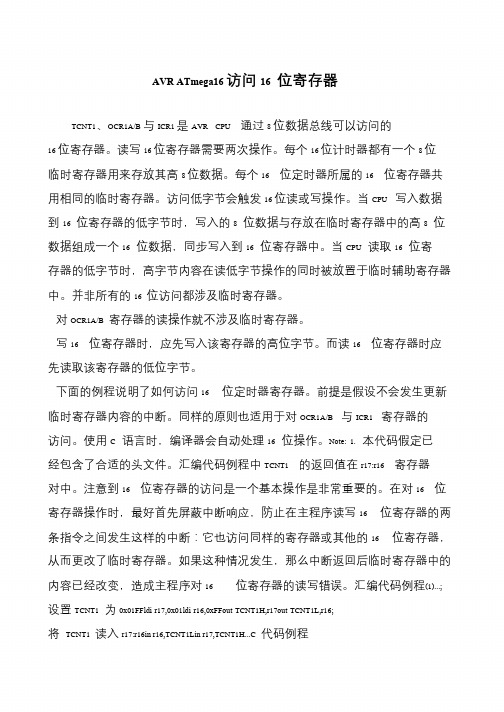
AVR单片机ATmega16最小系统电路图
编辑:D z3w.C o m文章来源:网络我们无意侵犯您的权益,如有侵犯
请[联系我们]
下面以本网站推荐的A V R入门芯片A T m e g a16L-8A I分析A V R单片机最小系统基本电路。
(-8A I表示8M频率的T Q F P贴片封装,工业级)
1.复位线路
2.晶振线路
3.A D转换滤波线路
4.I S P下载接口
5.J T A G仿真接口
6.电源
点击查看各部分原理分析
提示:点击图片看原图
M e g a16开发板外观图
我们将此设计图,制作成了以下的M e g a16功能小板。
以后我们网站的所有新手入门范例,及应用范例,大部分会以这块小板作为实验板。
正面图:晶振可以使用螺丝固定的方法更换,方便做实验,并达到一定
的可靠性。
V C C,G N D均有一测试针。
底部图:为了方便实验,我们将这块小板的输出脚,按直插A T m e g a16的管脚排列定义。
为防止不小心掉到地上导致插针折断,加装了一只40脚的圆孔I C座做保护。
如果不小心折断,可以方便地更换圆孔I C座。
ATmega16 熔丝位详解初学者对熔丝经常不解,AVR芯片使用熔丝来设定时钟、启动时间、一些功能的使能、BOOT区设定、当然还有最让初学者头疼的保密位,设不好锁了芯片很麻烦。
要想使MCU功耗最小也要了解一些位的设定在此写下自己对熔丝的理解,参照了一些MEGA16的PDF文档,双龙的文档,以及大家的帖子。
力求易懂、全面。
首先记住:1:未编程(检查框不打钩)0:编程(检查框打钩)建议在配置熔丝之前先“读取配置”读出原来的设定,再自己编辑。
看看M16的出厂设置。
默认设置为:内部RC振荡8MHZ 6 CK + 65 ms CKSEL=0100SUT=10高位:时钟及启动时间设置:BODLEVEL: BOD电平选择1:2.7V电平;0:4.0V电平BODEN: BOD功能控制, 1:BOD功能禁止;0:BOD功能允许使用方法:BOD(Brown-out Detection) 掉电检测电路,如果BODEN使能(编程)启动掉电检测,检测电平由BODLEVEL决定一旦VCC下降到触发电平(2.7v或4.0v)以下,MUC复位,当VCC 电平大于触发电平后,经过tTOUT 延时周后重新开始工作。
注:1:因为M16L可以工作在2.7v-5.5v所以触发电平可选2.7v或4.0v。
M16工作在4.5 - 5.5V,所以BODLEVEL=0。
BODLEVEL=1不适用于ATmega16,SUT1/0: 复位启动时间选择当选择不同晶振时,SUT有所不同。
如果没有特殊要求推荐SUT1/0设置电源缓慢上升。
CKSEL3/0: 时钟源选择低位:BOOT区设置JTAGEN: JTAG允许1:JTAG禁止;0:JTAG允许OCDEN:OCD功能允许1:OCD功能禁止;0:OCD功OCDEN(On-chip Debug)片上调试使能位,JTAGEN:JTAG使能JTAG 测试访问端口。
使用方法:在JTAG调试时使能OCDEN JTAGEN两位(打勾),并保持所有的锁定位处于非锁定状态,在实际使用时为降低功耗不使能OCDEN JTAGEN,大约减少2-3mA的电流。
A VR教程系列一(12):ATmega16 简介(六) ATmega16 操纵与状态寄存器MCUCSRAVR 操纵与状态寄存器提供了有关引起AVR复位的复位源的信息。
Bit 4 – JTRF: JTAG 复位标志通过JTAG 指令AVR_RESET 能够使JTAG 复位寄存器置位,并引发MCU 复位,并使JTRF 置位。
上电复位将使其清零,也能够通过写”0” 来清除。
Bit 3 – WDRF: 看门狗复位标志看门狗复位发生时置位。
上电复位将使其清零,也能够通过写”0” 来清除。
Bit 2 – BORF: 掉电检测复位标志掉电检测复位发生时置位。
上电复位将使其清零,也能够通过写”0” 来清除。
Bit 1 – EXTRF: 外部复位标志外部复位发生时置位。
上电复位将使其清零,也能够通过写”0” 来清除。
Bit 0 – PORF: 上电复位标志上电复位发生时置位。
只能通过写”0” 来清除。
为了使用这些复位标志来识别复位条件,用户应该尽早读取此寄存器的数据,然后将其复位。
假如在其他复位发生之前将此寄存器复位,则后续复位源能够通过检查复位标志来熟悉。
ATmega16 基准电压使能信号与启动时间ATmega16 具有片内能隙基准源,用于掉电检测,或者者是作为模拟比较器或者ADC的输入。
ADC 的2.56V 基准电压由此片内能隙基准源产生。
电压基准的启动时间可能影响其工作方式。
启动时间列于Table 16。
为了降低功耗,能够操纵基准源仅在如下情况打开:1. BOD 使能 ( 熔丝位BODEN 被编程)2. 能隙基准源连接到模拟比较器(ACSR 寄存器的ACBG 置位)3. ADC 使能因此,当BOD 被禁止时,置位ACBG 或者使能ADC 后要启动基准源。
为了降低掉电模式的功耗,用户能够禁止上述三种条件,并在进入掉电模式之前关闭基准源。
ATmega16 看门狗定时器看门狗定时器由独立的1 Mhz 片内振荡器驱动。
AVR单片机ATMEGA16 1602液晶驱动程序及心得首先,祝福各位同仁,光棍节快乐!今天,给我最好的节日礼物就是,我自己研发的AVR微控制器芯片开发板,1602液晶屏实验成功!我很欣慰.写了一整天的程序,反复实验,最终在凌晨0点.终于成功了.在此过程中,最大的问题莫过于那个所谓配套的1602液晶屏数据手册!这个手册简直是误人子弟,里面资料写的很含糊.并且有错误,而导致我反复试验失败,最终,我使用了通用的1602液晶屏数据手册,才得以成功.我自制的AVR开发板尺寸和我买的51开发板差不多大小,ATmega16最小系统,8位数码管,蓝光流水灯,isp编程接口.过载保护保险丝,两个74hc573锁存器.1602液晶屏都已焊接完成,万用板是12X18cm的单孔玻纤板(质量不太好,便宜没好货).现在我才发现不够用,模块数量相同的两块实验板,手工焊接的一定要比机器印刷的大2~3倍才行.....没办法,我只能用5X7cm的万用板做小模块,ADC模块,DS1302时钟模块,激光二极管模块等等,然后用杜邦线把它们和AVR核心板链接起来,目前计划是这样的,往往计划很丰满,实际很骨感,伤脑筋啊,,,此次,首次接触了12864大液晶,能显示中文,和超声波测距传感器,这得好好研究一下,我一直想要了解一下2.4g无线传输模块,和陀螺仪传感器,还有GPS模块,不过那些还早,把AVRATMEGA16学的差不多了,再了解,也不迟. /*Program name: AVR ATMEGA16 1602驱动程序初次实验通过时间: 2013-11-11 00:04:01 ^_^ ;注意:在bysy()函数中严重出错!下次注意!while((PINA&0x80)==0x80); 此语句检测到PA7为零时终止循环;表明空闲状态心得:AVR单片机的IO口位操作比较复杂,由三个寄存器控制IO口的输出与输入;DDRn(输出/输入控制) 寄存器;PORTn(输出时控制数据,输入时控制内部上拉电阻)寄存器;PINn(用于读取IO口数据)寄存器;最终校验通过时间: 2013年11月12日15:12:28*/#include ;#include ;#define uint8 unsigned char#define uint16 unsigned int//========IO口位操作========================================void rs(uint8 h)//数据/指令选择操作;{if(h)PORTB|=1<<3; //置一;elsePORTB&=~(1<<3); //清零; }void rw(uint8 h)//读/写选择操作;{if(h==0){PORTB&=~(1<<4); //清零;}else{DDRA=0X00;PORTA=0XFF;PORTB|=1<<4; //置一;}}void e(uint8 h)//传输使能位;{if(h){PORTB|=1<<5;//置一;}elsePORTB&=~(1<<5);//清零;}//=============================================== =========void ddra(uint8 h)//PA口输入输出函数;{if(h){DDRA=0XFF;//输出模式;PORTA=0xff;}else{DDRA=0X00; PORTA=0XFF; } //输入模式并且有上拉; }void busy()//繁忙检测;{ddra(0);//设置PA口为输入,有上拉;do{e(0);//传输使能为0;rs(0);//指令;rw(1);//读;e(1);//e为高电平;}while((PINA&0x80)==0x80);//如果读到数据是01111111,表示空闲状态,跳出循环;e(0);ddra(1);//PA口输出状态;}void delay() //小延时;{uint8 j=0;j=1;}void w_cmd(uint8 cmd){busy();//繁忙检测通过时,PA口为输出状态,默认输出0xff; PORTA=cmd; //向PA口装载数据;rs(0);//指令;rw(0);//写入;e(1);//传输使能脉冲高;delay();//延时;e(0);//传输使能脉冲低;}void w_dat(uint8 dat){busy();//繁忙检测通过时,PA口为输出状态,默认输出0xff; PORTA=dat; //向PA口装载数据;rs(1);//数据;rw(0);//写入;e(1);//传输使能脉冲高;delay();//延时;e(0);//传输使能脉冲低;}void init_1602(){w_cmd(0x3c); //写入显示设置:8位数据,两行,5x10显示;w_cmd(0x0c); //整屏显示,光标不闪,字符不闪; w_cmd(0x06); //写入一个数据时地址自动加一.整屏不移动;w_cmd(0x01); //写入'清屏'指令;}void display(uint8 addr ,uint8 dat )//可在任意位置显示字符,{//addr地址,dat数据;w_cmd(addr);w_dat(dat);}void main(void)//====主函数================={uint8 i=0, j=0x80,ak[]="I'am ironman!"; //要显示的字符串"我是钢铁侠!"uint8 sj[]="2013-11-11 ^_^"; //今天的日期;uint16 s=0;//16位的变量;DDRB=0XFF;//PB口输出状态;PORTB=0X03; //PB0=1;PB1=1;DDRA=0XFF;//PA口输出状态;PORTA=0X00;//8个数码管共阴极为'0'.八位阳极为'0'; PORTB=0X00;//锁存数据;init_1602();//液晶屏初始化;w_cmd(0x81); //初始化完成以后先发送要写入的数据的显示位置.//0x81是第一行,第1位. 0x80是第0位;while(ak[i]!='\0') //将ak[]数组内的所有数据发送; {w_dat(ak[i++]);//每发送一个字节数据,数据的存储地址自动加一; for(s=0;s<50000;s++); //延时一下,字符会有一个,一个显示的效果;}w_cmd(0xc1);//发送第二排的数据地址,接下来字符会在第二排第1位开始显示;i=0;while(sj[i]!='\0')//将sj[]数组内的数据全部发完;{w_dat(sj[i++]);for(s=0;s<25000;s++);//效果延时;}while(1);//死亡循环; }。
1AVR089: Migrating between ATmega16 andATmega32IntroductionThis application note is a guide to help current ATmega16 users convert existing designs to ATmega32. The information given will also help users migrating from ATmega32 to ATmega16. ATmega163 users should also read the application note “AVR083: Replacing A Tmega163 by ATmega16”.In addition to the differences described in this document, the electrical characteristics of the two devices are different. Check the data sheets for detailed information.Memory SizesAll the memories of the ATmega32 are bigger than those of the ATmega16. Table 1 is a comparision of the individual memories.The Boot Loader area is also changed. The following must be considered:•The No-Read-While-Write section starts at word address 0x3800 instead of 0x1C00.Table 1. Memory SizesATmega16ATmega32Flash 16k bytes 32k bytes RAM 1k bytes 2k bytes EEPROM512 bytes1k bytes8-bit Microcontroller2AVR0892538A–AVR–05/03Interrupt TablesThe ATmega32 has a different interrupt table from ATmega16. Table 2 compares the interrupt tables of the two devices.MiscellaneousThe following applies to ATmega32:•In the MCUCR Register, the SM2 and SE bits are swapped, i.e., SM2 is bit 7 and SE is bit 6.Table 2. Interrupt TableVector #ATmega16ATmega321RESET RESET 2INT0INT03INT1INT14TIMER2 COMP INT25TIMER2 OVF TIMER2 COMP 6TIMER1 CAPT TIMER2 OVF 7TIMER1 COMPA TIMER1 CAPT 8TIMER1 COMPB TIMER1 COMPA 9TIMER1 OVF TIMER1 COMPB 10TIMER0 OVF TIMER1 OVF 11SPI, STC TIMER0 COMP 12USART, RXC TIMER0 OVF 13USART, UDRE SPI, STC 14USART, TXC USART , RXC 15ADC USART , UDRE 16EE_RDY USART , TXC 17ANA_COMP ADC 18TWI EE_RDY 19INT2ANA_COMP 20TIMER0 COMP TWI 21SPM_RDYSPM_RDYDisclaimer: Atmel Corporation makes no warranty for the use of its products, other than those expressly contained in the Company’s standard warranty which is detailed in Atmel’s Terms and Conditions located on the Company’s web site. The Company assumes no responsibility for any errors which may appear in this document, reserves the right to change devices or specifications detailed herein at any time without notice, and does not make any commitment to update the information contained herein. No licenses to patents or other intellectual property of Atmel are granted by the Company in connection with the sale of Atmel products, expressly or by implication. Atmel’s products are not authorized for use as critical components in life support devices or systems.Atmel CorporationAtmel Operations2325 Orchard Parkway San Jose, CA 95131Tel: 1(408) 441-0311Fax: 1(408) 487-2600Regional HeadquartersEuropeAtmel SarlRoute des Arsenaux 41Case Postale 80CH-1705 Fribourg SwitzerlandTel: (41) 26-426-5555Fax: (41) 26-426-5500AsiaRoom 1219Chinachem Golden Plaza 77 Mody Road Tsimshatsui East Kowloon Hong KongTel: (852) 2721-9778Fax: (852) 2722-1369Japan9F, Tonetsu Shinkawa Bldg.1-24-8 ShinkawaChuo-ku, Tokyo 104-0033JapanTel: (81) 3-3523-3551Fax: (81) 3-3523-7581Memory2325 Orchard Parkway San Jose, CA 95131Tel: 1(408) 441-0311Fax: 1(408) 436-4314Microcontrollers2325 Orchard Parkway San Jose, CA 95131Tel: 1(408) 441-0311Fax: 1(408) 436-4314La Chantrerie BP 7060244306 Nantes Cedex 3, France Tel: (33) 2-40-18-18-18Fax: (33) 2-40-18-19-60ASIC/ASSP/Smart CardsZone Industrielle13106 Rousset Cedex, France Tel: (33) 4-42-53-60-00Fax: (33) 4-42-53-60-011150 East Cheyenne Mtn. Blvd.Colorado Springs, CO 80906Tel: 1(719) 576-3300Fax: 1(719) 540-1759Scottish Enterprise Technology Park Maxwell BuildingEast Kilbride G75 0QR, Scotland Tel: (44) 1355-803-000Fax: (44) 1355-242-743RF/AutomotiveTheresienstrasse 2Postfach 353574025 Heilbronn, Germany Tel: (49) 71-31-67-0Fax: (49) 71-31-67-23401150 East Cheyenne Mtn. Blvd.Colorado Springs, CO 80906Tel: 1(719) 576-3300Fax: 1(719) 540-1759Biometrics/Imaging/Hi-Rel MPU/High Speed Converters/RF DatacomAvenue de Rochepleine BP 12338521 Saint-Egreve Cedex, France Tel: (33) 4-76-58-30-00Fax: (33) 4-76-58-34-80e-mailliterature@Web Site2538A–AVR–05/030M© Atmel Corporation 2003. All rights reserved. Atmel ® and combinations thereof AVR ® are the registered trademarks of Atmel Corporation or its subsidiaries. Other terms and product names may be the trademarks of others.。