LCX059AKB中文文档部分翻译版
- 格式:pdf
- 大小:176.57 KB
- 文档页数:5

You want compact size and manoeuvrability. You want a machine that works in restricted height buildings. You want excellent lift height, lift capacity and reach. Before, all of this meant a combination of skid steer, wheeled loading shovel and forklift… not now. One machine, the JCB 515-40, ticks all the boxes, opening up telehandler versatility to a whole new range of users.So how does the 515-40 do it? One word… innovation. Everything hinges on our revolutionary, off-set, single-spine chassis which has its core strength under the boom and wraps around the cab. This allows us to position the cab lower than usual providing three key benefits.First, the whole machine is low, 1.8m in fact. Second, to achieve that height we haven’t had to shrink the cab, as in some competitor machines, so there’s no compromise on comfort or space. And third, cab entry is now at low level for improved health and safety.Despite mini proportions, the 515-40 packs a real punch, in line with customer feedback which told us you want compact dimensions, with power. So this incredible innovation can lift 1.5 tonnes to 4m height, and 1 tonne across 2m for loading the opposite side of a truck.Inside greenhouses, chicken sheds, tunnels and multi-storey car parks; craned into high-rise developments; a secondary site machine alongside your full-size Loadall; rental, builders’ merchants, fruit farms, smallholdings, vineyards: the 515-40 is the mini marvel we’ve all been waiting for.Innovation at its heart At 1.8m, it’s the ultimate, go-anywhere, mini marvelSo, the 515-40 can get in where doorways or building height often prove an obstacle to other machines. The same is true of a skid steer, you say. Y es, but often a skid steer can’t give access or loading height.At the same time, the 515-40 gives shovel performance comparable to a skid steer or wheeled loading shovel. Plus, individual hydraulic wheel motors and four-wheel steer equals superb movement in the face of tight corners, pillars and narrow doorways.Where ground conditions may vary, in builders’ merchants or farmyards, for instance, four-wheel drive and good ground clearance more than copes with the challenging terrain. Add a hydrostatic transmission for easy operation, infinite speed variations and better fuel efficiency, and you have the winning formula for versatile performance and productivity.The other feature that sets the 515-40 apart from its competitors is comfort. Thanks to the chassis design, there is no compromise on cab size to achieve the 1.8m height. So the interior is spacious with superb visibility.The stable-type door allows you to shut out unpleasant conditions, or open up the top half for a little fresh air whilst still protecting the operator from mud and debris. Optional air conditioning or face level fan further enhance operator comfort. And the cab itself, with side, low-level entry, also means the 515-40 is a safer machine.You’ve got it into a tight space,now what?Incredible manoeuvrability, performance and comfort…that’s whatMachine model515-40Main service pump operating system pressure bar (psi) 230 (3336)Flow at system pressure (@ 2800rpm) ltr/min (gal/min) 47.6 (10.5)Maximum auxiliary flow (@ 230bar) ltr/min (gal/min)47.6 (10.21)Cycle times seconds Boom raise 7.3Boom lower 5.4Extend 5.8Retract 3.7Bucket dump 2.8Bucket crowd3.9HYDRAULICSHydrostatic transmission.Closed loop variable displacement piston pump with twin displacement transmission wheel motors.Transmission inching facility on operation of a combined inching and braking pedal.Front and rear drive axles: Permanent 4WS and 4WD.– Rear axle oscillation.– Automatic torque transfer system between front and back axles.– Maximum travel speed 20kph (12.4mph).TRANSMISSIONService brake: Hydraulically activated, drum brake on the front wheel motors.Parking brake: Manually operated drum brake on the front wheel motors.BRAKESBoom is manufactured from high tensile steel.Low maintenance, hard wearing pads.JCB tool carrier parallel lift carriage with manual pin locking, accepts forkframe with integral pallet forks and a wide range of attachments.Compact Tool Carrier: Compact Loadall compatibility.Skid Steer Tool Carrier: Skid steer universal compatibility hitch.BOOM AND CARRIAGEFitted to crowd, extension and lift rams.SAFETY CHECK VALVES12 V negative earth, 60 AH heavy-duty battery. 80 amp alternator.ELECTRICSQuiet, safe and comfortable cab conforms to ROPS ISO3471 and FOPS ISO 3449. Internal noise 85 Lpa. Radio console. Arm rest. Tinted glass all round with laminated front and roof screen. Front, rear screen wash/wipe and heater/screen demister. Opening door window. Optional air conditioning or face-level fan. Visual warning system for coolant temperature, engine oil pressure, air cleaner, battery charge, transmission oil pressure, engine temperature, fuel gauge and hourmeter.Boom control lever incorporating forward/reverse switch. Throttle and brake pedals floor mounted. Optional fabric or vinyl adjustable. Adjustable deluxe suspension seat with side mounted park brake lever. Automatic eye level audio-visual loadmoment indicator warning system receiving a signal from a load sensor on the rear axle. This system continuously monitors the machine’s forward stability and leaves the operator in control at all times.CABFull hydrostatic power steering. Permanent 4WS with 32° lock front and rear axles provides exceptional manoeuvrability.STEERINGOptions: Road lights, work lights, rotating flashing beacon, fire extinguisher, front screen guard, sun blind, traction, industrial orsemi-turf tyres, chaff guard, canopy, mechanical compact loadall quickhitch or and Skid Steer quickhitch, battery isolator, industrial or semi-turf tyres, chaff guards, canopy. Cab options : Air conditioning, face level fan, opening door window, screen guard.Attachments: Compact loadall quickhitch: GP shovel with teeth or toeplate, industrial or floating forks, bale spike, power grab. OPTIONS AND ACCESSORIESlitres (UK gal)Fuel tank 50 (11)SERVICE CAPACITIESENGINE515-40Model Deutz D2009L04Displacement litres2.3 Fuel Diesel CoolingLiquid Bore mm (in) 90 (3.5)Strokemm (in)90 (3.5)Gross power @ 2800 rpmISO 14396kW (hp)36.8 (50)Gross torque @ 1800 rpmISO 14396Nm (lb/ft)146 (107.68)Emission certification EC Stage IIIA/USA EPA Tier 3Engine oil service intervals500 hoursJCB Sales Limited, Rocester, Staffordshire, United Kingdom ST14 5JP. Tel: +44 (0)1889590312Email:***************** Download the very latest information on this product range at: 。
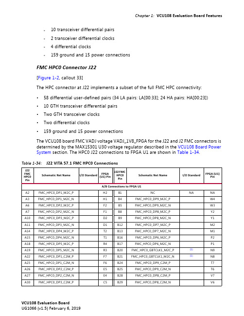
°10 transceiver differential pairs° 2 transceiver differential clocks° 4 differential clocks°159 ground and 15 power connectionsFMC HPC0 Connector J22[Figure1-2, callout 33]The HPC connector at J22 implements a subset of the full FMC HPC connectivity:•58 differential user-defined pairs (34 LA pairs: LA[00:33]; 24 HA pairs: HA[00:23])•10 GTH transceiver differential pairs•Two GTH transceiver clocks•Two differential clocks•159 ground and 15 power connectionsThe VCU108 board FMC VADJ voltage VADJ_1V8_FPGA for the J22 and J2 FMC connectors is determined by the MAX15301 U30 voltage regulator described in the VCU108 Board Power System section. The HPC0 J22 connections to FPGA U1 are shown in Table1-34.Table 1-34:J22 VITA 57.1 FMC HPC0 ConnectionsJ22FMC HPC0 Pin Schematic Net Name I/O Standard FPGA(U1) PinJ22 FMCHPC0PinSchematic Net Name I/O Standard FPGA (U1)PinA/B Connections to FPGA U1A2 FMC_HPC0_DP1_M2C_P H2B1NC NA NA A3 FMC_HPC0_DP1_M2C_N H1B4 FMC_HPC0_DP9_M2C_P W4 A6 FMC_HPC0_DP2_M2C_P F2B5FMC_HPC0_DP9_M2C_N W3 A7 FMC_HPC0_DP2_M2C_N F1B8 FMC_HPC0_DP8_M2C_P Y2 A10 FMC_HPC0_DP3_M2C_P D2B9FMC_HPC0_DP8_M2C_N Y1 A11 FMC_HPC0_DP3_M2C_N D1B12FMC_HPC0_DP7_M2C_P M2 A14 FMC_HPC0_DP4_M2C_P T2B13FMC_HPC0_DP7_M2C_N M1 A15 FMC_HPC0_DP4_M2C_N T1B16FMC_HPC0_DP6_M2C_P P2 A18 FMC_HPC0_DP5_M2C_P R4B17FMC_HPC0_DP6_M2C_N P1 A19 FMC_HPC0_DP5_M2C_N R3B20FMC_HPC0_GBTCLK1_M2C_P(1)N9 A22 FMC_HPC0_DP1_C2M_P F7B21FMC_HPC0_GBTCLK1_M2C_N(1)N8 A23 FMC_HPC0_DP1_C2M_N F6B24FMC_HPC0_DP9_C2M_P T7 A26 FMC_HPC0_DP2_C2M_P E5B25FMC_HPC0_DP9_C2M_N T6 A27 FMC_HPC0_DP2_C2M_N E4B28FMC_HPC0_DP8_C2M_P V7 A30 FMC_HPC0_DP3_C2M_P C5B29FMC_HPC0_DP8_C2M_N V6E/F Connections to FPGA U1E2 FMC_HPC0_HA01_CC_P LVDS T14F1 FMC_HPC0_PG_M2C (7)LVCMOS18U44.18E3 FMC_HPC0_HA01_CC_N LVDS R13F4 FMC_HPC0_HA00_CC_P LVDS N14E6FMC_HPC0_HA05_P LVDS AA12F5FMC_HPC0_HA00_CC_N LVDS N13E7FMC_HPC0_HA05_N LVDS Y12F7FMC_HPC0_HA04_P LVDS AA13E9FMC_HPC0_HA09_P LVDS AA14F8FMC_HPC0_HA04_N LVDS Y13E10FMC_HPC0_HA09_N LVDS Y14F10FMC_HPC0_HA08_P LVDS W12E12FMC_HPC0_HA13_P LVDS W14F11FMC_HPC0_HA08_N LVDS V12E13FMC_HPC0_HA13_N LVDS V14F13FMC_HPC0_HA12_P LVDS V15E15FMC_HPC0_HA16_P LVDS V16F14FMC_HPC0_HA12_N LVDS U15E16FMC_HPC0_HA16_NLVDSU16F16FMC_HPC0_HA15_PLVDSV13Table 1-34:J22 VITA 57.1 FMC HPC0 Connections (Cont’d)J22 FMC HPC0 PinSchematic Net NameI/O StandardFPGA (U1) PinJ22 FMC HPC0 PinSchematic Net NameI/O StandardFPGA (U1)PinG13FMC_HPC0_LA08_NLVDS BF9H11FMC_HPC0_LA04_N LVDS BE7G15FMC_HPC0_LA12_P LVDS BE15H13FMC_HPC0_LA07_P LVDS BD12G16FMC_HPC0_LA12_N LVDS BF15H14FMC_HPC0_LA07_N LVDS BE12G18FMC_HPC0_LA16_P LVDS AY8H16FMC_HPC0_LA11_P LVDS BC11G19FMC_HPC0_LA16_N LVDS AY7H17FMC_HPC0_LA11_N LVDS BD11G21FMC_HPC0_LA20_P LVDS AY15H19FMC_HPC0_LA15_P LVDS AV9G22FMC_HPC0_LA20_N LVDS AY14H20FMC_HPC0_LA15_N LVDS AV8G24FMC_HPC0_LA22_P LVDS AN15H22FMC_HPC0_LA19_P LVDS AV15G25FMC_HPC0_LA22_N LVDS AP15H23FMC_HPC0_LA19_N LVDS AW15G27FMC_HPC0_LA25_P LVDS AM13H25FMC_HPC0_LA21_P LVDS AN16G28FMC_HPC0_LA25_N LVDS AM12H26FMC_HPC0_LA21_N LVDS AP16G30FMC_HPC0_LA29_P LVDS AK14H28FMC_HPC0_LA24_P LVDS AK15G31FMC_HPC0_LA29_N LVDS AK13H29FMC_HPC0_LA24_N LVDS AL15G33FMC_HPC0_LA31_P LVDS AP12H31FMC_HPC0_LA28_P LVDS AJ13G34FMC_HPC0_LA31_NLVDSAR12H32FMC_HPC0_LA28_NLVDSAJ12Table 1-34:J22 VITA 57.1 FMC HPC0 Connections (Cont’d)J22 FMC HPC0 Pin Schematic Net Name I/O StandardFPGA (U1) Pin J22 FMC HPC0 Pin Schematic Net Name I/O StandardFPGA (U1)PinThe VCU108 evaluation board uses power regulators and PMBus compliant PoL controllers from Maxim Integrated Circuits to supply the core and auxiliary voltages listed inTable1-36.Table 1-36:Onboard Power System DevicesDevice Type ReferenceDesignator PMBusAddress DescriptionPower Rail NetNamePower RailVoltageMAX20751EKX U1640x70Maxim multiphase masterwith smart slavesVT1697SBFQX 60AVCCINT_FPGA0.95VMAX15301U90x11Maxim InTune digital POLcontroller 10A VCC1V8_FPGA 1.80VMAX15301U300x12Maxim InTune digital POLcontroller 10A VADJ_1V8_FPGA 1.80VMAX15301U40x14Maxim InTune digital POLcontroller 10A VCC1V2_FPGA 1.20VMAX20751EKX U1660x72Maxim multiphase masterwith smart slaveVT1697SBFQX 17AMGTAVCC_FPGA 1.00VMAX20751EKX U1650x73Maxim multiphase masterwith smart slaveVT1697SBFQX 17AMGTAVTT_FPGA 1.20VMAX8869EUE U167NA Maxim fixed LDO 1A MGTVCCAUX 1.80VMAX15301U1500x1A Maxim InTune digital POLcontroller 10A UTIL_1V35 1.35VMAX15301U1560x1B Maxim InTune digital POLcontroller 20A UTIL_3V3 3.30VMAX17502U82NA Maxim synchronous buckswitcher 1A SYS_5V0 5.00VMAX15053U124NA Maxim adjustablesynchronous buck switcher2ASYS_1V0 1.00VMAX15027U125NA Maxim adjustable LDO 1A SYS_1V8 1.80VMAX15053U151NA Maxim adjustablesynchronous buck switcher2ASYS_2V5 2.50VTPS51200U24NA TI source-sink V TT regulator3A DDR4_C1_VTT0.60VTPS51200U134NA TI source-sink V TT regulator3A DDR4_C2_VTT0.60VTPS51200U143NA TI source-sink V TT regulator3A RLD3_C1_VTERM0.60V。
© 2001 Xilinx, Inc. All rights reserved. All Xilinx trademarks, registered trademarks, patents, and disclaimers are as listed at /legal.htm .All other trademarks and registered trademarks are the property of their respective owners. All specifications are subject to change without notice.IntroductionThe Spartan ™ and the Spartan-XL families are a high-vol-ume production FPGA solution that delivers all the key requirements for ASIC replacement up to 40,000 gates.These requirements include high performance, on-chip RAM, core solutions and prices that, in high volume,approach and in many cases are equivalent to mask pro-grammed ASIC devices.The Spartan series is the result of more than 14 years of FPGA design experience and feedback from thousands of customers. By streamlining the Spartan series feature set,leveraging advanced process technologies and focusing on total cost management, the Spartan series delivers the key features required by ASIC and other high-volume logic users while avoiding the initial cost, long development cycles and inherent risk of conventional ASICs. The Spar-tan and Spartan-XL families in the Spartan series have ten members, as shown in T able 1.Spartan and Spartan-XL FeaturesNote: The Spartan series devices described in this data sheet include the 5V Spartan family and the 3.3V Spartan-XL family. See the separate data sheet for the 2.5V Spartan-II family.•First ASIC replacement FPGA for high-volume production with on-chip RAM•Density up to 1862 logic cells or 40,000 system gates •Streamlined feature set based on XC4000 architecture •System performance beyond 80MHz•Broad set of AllianceCORE ™ and LogiCORE ™ predefined solutions available •Unlimited reprogrammability •Low cost•System level features-Available in both 5V and 3.3V versions -On-chip SelectRAM ™ memory -Fully PCI compliant-Full readback capability for program verificationand internal node observability -Dedicated high-speed carry logic -Internal 3-state bus capability-Eight global low-skew clock or signal networks -IEEE 1149.1-compatible Boundary Scan logic -Low cost plastic packages available in all densities -Footprint compatibility in common packages•Fully supported by powerful Xilinx development system -Foundation Series: Integrated, shrink-wrapsoftware-Alliance Series: Dozens of PC and workstationthird party development systems supported-Fully automatic mapping, placement and routing Additional Spartan-XL Features• 3.3V supply for low power with 5V tolerant I/Os •Power down input •Higher performance •Faster carry logic•More flexible high-speed clock network•Latch capability in Configurable Logic Blocks •Input fast capture latch•Optional mux or 2-input function generator on outputs •12 mA or 24 mA output drive •5V and 3.3V PCI compliant •Enhanced Boundary Scan •Express Mode configuration •Chip scale packagingSpartan and Spartan-XL Families Field Programmable Gate ArraysDS060 (v1.6) September 19, 2001Product Specification T able 1: Spartan and Spartan-XL Field Programmable Gate Arrays1.Max values of Typical Gate Range include 20-30% of CLBs used as RAM.2DS060 (v1.6) September 19, 2001General OverviewSpartan series FPGAs are implemented with a regular, flex-ible, programmable architecture of Configurable Logic Blocks (CLBs), interconnected by a powerful hierarchy of versatile routing resources (routing channels), and sur-rounded by a perimeter of programmable Input/Output Blocks (IOBs), as seen in Figure 1. They have generous routing resources to accommodate the most complex inter-connect patterns.The devices are customized by loading configuration data into internal static memory cells. Re-programming is possi-ble an unlimited number of times. The values stored in thesememory cells determine the logic functions and intercon-nections implemented in the FPGA. The FPGA can either actively read its configuration data from an external serial PROM (Master Serial mode), or the configuration data can be written into the FPGA from an external device (Slave Serial mode).Spartan series FPGAs can be used where hardware must be adapted to different user applications. FPGAs are ideal for shortening design and development cycles, and also offer a cost-effective solution for production rates well beyond 50,000 systems per month.Figure 1: Basic FPGA Block DiagramSpartan series devices achieve high-performance, low-cost operation through the use of an advanced architecture and semiconductor technology. Spartan and Spartan-XL devices provide system clock rates exceeding 80MHz and internal performance in excess of150MHz. In contrast to other FPGA devices, the Spartan series offers the most cost-effective solution while maintaining leading-edge per-formance. In addition to the conventional benefit of high vol-ume programmable logic solutions, Spartan series FPGAs also offer on-chip edge-triggered single-port and dual-port RAM, clock enables on all flip-flops, fast carry logic, and many other features.The Spartan/XL families leverage the highly successful XC4000 architecture with many of that family’s features and benefits. T echnology advancements have been derived from the XC4000XLA process developments.Logic Functional DescriptionThe Spartan series uses a standard FPGA structure as shown in Figure1, page2. The FPGA consists of an array of configurable logic blocks (CLBs) placed in a matrix of routing channels. The input and output of signals is achieved through a set of input/output blocks (IOBs) forming a ring around the CLBs and routing channels.•CLBs provide the functional elements for implementing the user’s logic.•IOBs provide the interface between the package pins and internal signal lines.•Routing channels provide paths to interconnect the inputs and outputs of the CLBs and IOBs.The functionality of each circuit block is customized during configuration by programming internal static memory cells. The values stored in these memory cells determine the logic functions and interconnections implemented in the FPGA.Configurable Logic Blocks (CLBs)The CLBs are used to implement most of the logic in an FPGA. The principal CLB elements are shown in the simpli-fied block diagram in Figure2. There are three look-up tables (LUT) which are used as logic function generators, two flip-flops and two groups of signal steering multiplexers. There are also some more advanced features provided by the CLB which will be covered in the Advanced Features Description, page13.Function GeneratorsTwo 16x1 memory look-up tables (F-LUT and G-LUT) are used to implement 4-input function generators, each offer-ing unrestricted logic implementation of any Boolean func-tion of up to four independent input signals (F1 to F4 or G1 to G4). Using memory look-up tables the propagation delay is independent of the function implemented.A third 3-input function generator (H-LUT) can implement any Boolean function of its three inputs. Two of these inputs are controlled by programmable multiplexers (see box "A" of Figure2). These inputs can come from the F-LUT or G-LUT outputs or from CLB inputs. The third input always comes from a CLB input. The CLB can, therefore, implement cer-tain functions of up to nine inputs, like parity checking. The three LUTs in the CLB can also be combined to do any arbi-trarily defined Boolean function of five inputs.4DS060 (v1.6) September 19, 2001A CLB can implement any of the following functions:•Any function of up to four variables, plus any second function of up to four unrelated variables, plus any third function of up to three unrelated variablesNote: When three separate functions are generated, one of the function outputs must be captured in a flip-flop internal to the CLB. Only two unregistered function generator outputs are available from the CLB.•Any single function of five variables•Any function of four variables together with some functions of six variables•Some functions of up to nine variables.Implementing wide functions in a single block reduces both the number of blocks required and the delay in the signal path, achieving both increased capacity and speed. The versatility of the CLB function generators significantly improves system speed. In addition, the design-software tools can deal with each function generator independently.This flexibility improves cell usage.Flip-FlopsEach CLB contains two flip-flops that can be used to regis-ter (store) the function generator outputs. The flip-flops and function generators can also be used independently (see Figure 2). The CLB input DIN can be used as a direct input to either of the two flip-flops. H1 can also drive either flip-flop via the H-LUT with a slight additional delay.The two flip-flops have common clock (CK), clock enable (EC) and set/reset (SR) inputs. Internally both flip-flops are also controlled by a global initialization signal (GSR) which is described in detail in Global Signals: GSR and GTS ,page 20.Latches (Spartan-XL only)The Spartan-XL CLB storage elements can also be config-ured as latches. The two latches have common clock (K)and clock enable (EC) inputs. Functionality of the storage element is described in Table 2.Figure 2: Spartan/XL Simplified CLB Logic Diagram (some features not shown)Clock InputEach flip-flop can be triggered on either the rising or falling clock edge. The CLB clock line is shared by both flip-flops.However, the clock is individually invertible for each flip-flop (see CK path in Figure 3). Any inverter placed on the clock line in the design is automatically absorbed into the CLB. Clock EnableThe clock enable line (EC) is active High. The EC line is shared by both flip-flops in a CLB. If either one is left discon-nected, the clock enable for that flip-flop defaults to the active state. EC is not invertible within the CLB. The clock enable is synchronous to the clock and must satisfy the setup and hold timing specified for the device.Set/ResetThe set/reset line (SR) is an asynchronous active High con-trol of the flip-flop. SR can be configured as either set or reset at each flip-flop. This configuration option determines the state in which each flip-flop becomes operational after configuration. It also determines the effect of a GSR pulse during normal operation, and the effect of a pulse on the SR line of the CLB. The SR line is shared by both flip-flops. If SR is not specified for a flip-flop the set/reset for that flip-flop defaults to the inactive state. SR is not invertible within the CLB.CLB Signal Flow ControlIn addition to the H-LUT input control multiplexers (shown in box "A" of Figure 2, page 4) there are signal flow control multiplexers (shown in box "B" of Figure 2) which select the signals which drive the flip-flop inputs and the combinatorial CLB outputs (X and Y).Each flip-flop input is driven from a 4:1 multiplexer which selects among the three LUT outputs and DIN as the data source.Each combinatorial output is driven from a 2:1 multiplexer which selects between two of the LUT outputs. The X output can be driven from the F-LUT or H-LUT, the Y output from G-LUT or H-LUT .Control SignalsThere are four signal control multiplexers on the input of the CLB. These multiplexers allow the internal CLB control sig-nals (H1, DIN, SR, and EC in Figure 2 and Figure 4) to be driven from any of the four general control inputs (C1-C4 in Figure 4) into the CLB. Any of these inputs can drive any of the four internal control signals.T able 2: CLB Storage Element FunctionalityLegend:XDon ’t careRising edge (clock not inverted).SR Set or Reset value. Reset is default.0*Input is Low or unconnected (default value)1*Input is High or unconnected (default value)Figure 3: CLB Flip-Flop Functional Block Diagram6DS060 (v1.6) September 19, 2001The four internal control signals are:•EC: Enable Clock•SR: Asynchronous Set/Reset or H function generator Input 0•DIN: Direct In or H function generator Input 2•H1: H function generator Input 1.Input/Output Blocks (IOBs)User-configurable input/output blocks (IOBs) provide the interface between external package pins and the internal logic. Each IOB controls one package pin and can be con-figured for input, output, or bidirectional signals. Figure 6shows a simplified functional block diagram of the Spar-tan/XL IOB.IOB Input Signal PathThe input signal to the IOB can be configured to either go directly to the routing channels (via I1 and I2 in Figure 6) or to the input register. The input register can be programmed as either an edge-triggered flip-flop or a level-sensitive latch. The functionality of this register is shown in Table 3,and a simplified block diagram of the register can be seen in Figure 5.Figure 4: CLB Control Signal InterfaceFigure 5: IOB Flip-Flop/Latch Functional BlockDiagramTable 3: Input Register FunctionalityX Don ’t care.Rising edge (clock not inverted).SR Set or Reset value. Reset is default.0*Input is Low or unconnected (default value)1*Input is High or unconnected (default value)The register choice is made by placing the appropriate library symbol. For example, IFD is the basic input flip-flop (rising edge triggered), and ILD is the basic input latch (transparent-High). Variations with inverted clocks are also available. The clock signal inverter is also shown in Figure5 on the CK line.The Spartan IOB data input path has a one-tap delay ele-ment: either the delay is inserted (default), or it is not. The Spartan-XL IOB data input path has a two-tap delay ele-ment, with choices of a full delay, a partial delay, or no delay. The added delay guarantees a zero hold time with respect to clocks routed through the global clock buffers. (See Glo-bal Nets and Buffers, page12 for a description of the glo-bal clock buffers in the Spartan/XL families.) For a shorter input register setup time, with positive hold-time, attach a NODELAY attribute or property to the flip-flop.The output of the input register goes to the routing channels (via I1 and I2 in Figure6). The I1 and I2 signals that exit the IOB can each carry either the direct or registered input signal.The 5V Spartan input buffers can be globally configured for either TTL (1.2V) or CMOS (VCC/2) thresholds, using an option in the bitstream generation software. The Spartan output levels are also configurable; the two global adjust-ments of input threshold and output level are independent. The inputs of Spartan devices can be driven by the outputs of any 3.3V device, if the Spartan inputs are in TTL mode. Input and output thresholds are TTL on all configuration pins until the configuration has been loaded into the device and specifies how they are to be used. Spartan-XL inputs are TTL compatible and 3.3V CMOS compatible. Supported sources for Spartan/XL device inputs are shown in Table4.Spartan-XL I/Os are fully 5V tolerant even though the V CC is 3.3V. This allows 5V signals to directly connect to the Spar-tan-XL inputs without damage, as shown in Table4. In addi-tion, the 3.3V V CC can be applied before or after 5V signals are applied to the I/Os. This makes the Spartan-XL devices immune to power supply sequencing problems.Figure 6: Simplified Spartan/XL IOB Block Diagram8DS060 (v1.6) September 19, 2001Spartan-XL V CC ClampingSpartan-XL FPGAs have an optional clamping diode con-nected from each I/O to V CC . When enabled they clamp ringing transients back to the 3.3V supply rail. This clamping action is required in 3.3V PCI applications. V CC clamping is a global option affecting all I/O pins.Spartan-XL devices are fully 5V TTL I/O compatible if V CC clamping is not enabled. With V CC clamping enabled, the Spartan-XL devices will begin to clamp input voltages to one diode voltage drop above V CC . If enabled, TTL I/O com-patibility is maintained but full 5V I/O tolerance is sacrificed.The user may select either 5V tolerance (default) or 3.3V PCI compatibility. In both cases negative voltage is clamped to one diode voltage drop below ground.Spartan-XL devices are compatible with TTL, LVTTL, PCI 3V, PCI 5V and LVCMOS signalling. The various standards are illustrated in Table 5.Additional Fast Capture Input Latch (Spartan-XL only)The Spartan-XL IOB has an additional optional latch on the input. This latch is clocked by the clock used for the output flip-flop rather than the input clock. Therefore, two different clocks can be used to clock the two input storage elements.This additional latch allows the fast capture of input data,which is then synchronized to the internal clock by the IOB flip-flop or latch.T o place the Fast Capture latch in a design, use one of the special library symbols, ILFFX or ILFLX. ILFFX is a trans-parent-Low Fast Capture latch followed by an active High input flip-flop. ILFLX is a transparent Low Fast Capture latch followed by a transparent High input latch. Any of the clock inputs can be inverted before driving the library element,and the inverter is absorbed into the IOB.IOB Output Signal PathOutput signals can be optionally inverted within the IOB,and can pass directly to the output buffer or be stored in an edge-triggered flip-flop and then to the output buffer. The functionality of this flip-flop is shown in T able 6.T able 4: Supported Sources for Spartan/XL InputsT able 5: I/O Standards Supported by Spartan-XL FPGAsTable 6: Output Flip-Flop Functionality X Don ’t careRising edge (clock not inverted). SR Set or Reset value. Reset is default.0*Input is Low or unconnected (default value)1*Input is High or unconnected (default value)Z3-stateOutput Multiplexer/2-Input Function Generator (Spartan-XL only)The output path in the Spartan-XL IOB contains an addi-tional multiplexer not available in the Spartan IOB. The mul-tiplexer can also be configured as a 2-input function generator, implementing a pass gate, AND gate, OR gate, or XOR gate, with 0, 1, or 2 inverted inputs.When configured as a multiplexer, this feature allows two output signals to time-share the same output pad, effec-tively doubling the number of device outputs without requir-ing a larger, more expensive package. The select input is the pin used for the output flip-flop clock, OK.When the multiplexer is configured as a 2-input function generator, logic can be implemented within the IOB itself. Combined with a Global buffer, this arrangement allows very high-speed gating of a single signal. For example, a wide decoder can be implemented in CLBs, and its output gated with a Read or Write Strobe driven by a global buffer. The user can specify that the IOB function generator be used by placing special library symbols beginning with the letter "O." For example, a 2-input AND gate in the IOB func-tion generator is called OAND2. Use the symbol input pin labeled "F" for the signal on the critical path. This signal is placed on the OK pin — the IOB input with the shortest delay to the function generator. Two examples are shown in Figure7.Output BufferAn active High 3-state signal can be used to place the out-put buffer in a high-impedance state, implementing 3-state outputs or bidirectional I/O. Under configuration control, the output (O) and output 3-state (T) signals can be inverted. The polarity of these signals is independently configured for each IOB (see Figure6, page7). An output can be config-ured as open-drain (open-collector) by tying the 3-state pin (T) to the output signal, and the input pin (I) to Ground.By default, a 5V Spartan device output buffer pull-up struc-ture is configured as a TTL-like totem-pole. The High driver is an n-channel pull-up transistor, pulling to a voltage one transistor threshold below V CC. Alternatively, the outputs can be globally configured as CMOS drivers, with additional p-channel pull-up transistors pulling to V CC. This option, applied using the bitstream generation software, applies to all outputs on the device. It is not individually programma-ble.All Spartan-XL device outputs are configured as CMOS drivers, therefore driving rail-to-rail. The Spartan-XL outputs are individually programmable for 12mA or 24mA output drive.Any 5V Spartan device with its outputs configured in TTL mode can drive the inputs of any typical 3.3V device. Sup-ported destinations for Spartan/XL device outputs are shown in Table7.Three-State Register (Spartan-XL Only)Spartan-XL devices incorporate an optional register control-ling the three-state enable in the IOBs. The use of the three-state control register can significantly improve output enable and disable time.Output Slew RateThe slew rate of each output buffer is, by default, reduced, to minimize power bus transients when switching non-criti-cal signals. For critical signals, attach a FAST attribute or property to the output buffer or flip-flop.Spartan/XL devices have a feature called "Soft Start-up," designed to reduce ground bounce when all outputs are turned on simultaneously at the end of configuration. When the configuration process is finished and the device starts up, the first activation of the outputs is automatically slew-rate limited. Immediately following the initial activation of the I/O, the slew rate of the individual outputs is deter-mined by the individual configuration option for each IOB. Pull-up and Pull-down NetworkProgrammable pull-up and pull-down resistors are used fortying unused pins to V CC or Ground to minimize power con-sumption and reduce noise sensitivity. The configurablepull-up resistor is a p-channel transistor that pulls to V CC.The configurable pull-down resistor is an n-channel transis-tor that pulls to Ground. The value of these resistors is typi-cally 20KΩ − 100KΩ (See "Spartan DC Characteristics Figure 7: AND and MUX Symbols in Spartan-XL IOB10DS060 (v1.6) September 19, 2001Over Operating Conditions" on page 43.). This high value makes them unsuitable as wired-AND pull-up resistors.After configuration, voltage levels of unused pads, bonded or unbonded, must be valid logic levels, to reduce noise sensitivity and avoid excess current. Therefore, by default,unused pads are configured with the internal pull-up resistor active. Alternatively, they can be individually configured with the pull-down resistor, or as a driven output, or to be driven by an external source. To activate the internal pull-up, attach the PULLUP library component to the net attached to the pad. To activate the internal pull-down, attach the PULL-DOWN library component to the net attached to the pad.Set/ResetAs with the CLB registers, the GSR signal can be used to set or clear the input and output registers, depending on the value of the INIT attribute or property. The two flip-flops can be individually configured to set or clear on reset and after configuration. Other than the global GSR net, no user-con-trolled set/reset signal is available to the I/O flip-flops (Figure 5). The choice of set or reset applies to both the ini-tial state of the flip-flop and the response to the GSR pulse.Independent ClocksSeparate clock signals are provided for the input (IK) and output (OK) flip-flops. The clock can be independently inverted for each flip-flop within the IOB, generating eitherfalling-edge or rising-edge triggered flip-flops. The clock inputs for each IOB are mon Clock EnablesThe input and output flip-flops in each IOB have a common clock enable input (see EC signal in Figure 5), which through configuration, can be activated individually for the input or output flip-flop, or both. This clock enable operates exactly like the EC signal on the Spartan/XL CLB. It cannot be inverted within the IOB.Routing Channel DescriptionAll internal routing channels are composed of metal seg-ments with programmable switching points and switching matrices to implement the desired routing. A structured,hierarchical matrix of routing channels is provided to achieve efficient automated routing.This section describes the routing channels available in Spartan/XL devices. Figure 8 shows a general block dia-gram of the CLB routing channels. The implementation soft-ware automatically assigns the appropriate resources based on the density and timing requirements of the design.The following description of the routing channels is for infor-mation only and is simplified with some minor details omit-ted. For an exact interconnect description the designer should open a design in the FPGA Editor and review the actual connections in this tool.The routing channels will be discussed as follows;•CLB routing channels which run along each row and column of the CLB array.•IOB routing channels which form a ring (called a VersaRing) around the outside of the CLB array. It connects the I/O with the CLB routing channels.•Global routing consists of dedicated networks primarily designed to distribute clocks throughout the device with minimum delay and skew. Global routing can also be used for other high-fanout signals.CLB Routing ChannelsThe routing channels around the CLB are derived from three types of interconnects; single-length, double-length,and longlines. At the intersection of each vertical and hori-zontal routing channel is a signal steering matrix called a Programmable Switch Matrix (PSM). Figure 8 shows the basic routing channel configuration showing single-length lines, double-length lines and longlines as well as the CLBs and PSMs. The CLB to routing channel interface is shown as well as how the PSMs interface at the channel intersec-tions.T able 7: Supported Destinations for Spartan/XL OutputsNotes:1.Only if destination device has 5V tolerant inputs.CLB InterfaceA block diagram of the CLB interface signals is shown in Figure9. The input signals to the CLB are distributed evenly on all four sides providing maximum routing flexibility. In general, the entire architecture is symmetrical and regular. It is well suited to established placement and routing algo-rithms. Inputs, outputs, and function generators can freely swap positions within a CLB to avoid routing congestion during the placement and routing operation. The exceptions are the clock (K) input and CIN/COUT signals. The K input is routed to dedicated global vertical lines as well as four single-length lines and is on the left side of the CLB. The CIN/COUT signals are routed through dedicated intercon-nects which do not interfere with the general routing struc-ture. The output signals from the CLB are available to drive both vertical and horizontal channels.Programmable Switch MatricesThe horizontal and vertical single- and double-length lines intersect at a box called a programmable switch matrix (PSM). Each PSM consists of programmable pass transis-tors used to establish connections between the lines (see Figure10).For example, a single-length signal entering on the right side of the switch matrix can be routed to a single-length line on the top, left, or bottom sides, or any combination thereof, if multiple branches are required. Similarly, a dou-ble-length signal can be routed to a double-length line on any or all of the other three edges of the programmable switch matrix.Single-Length LinesSingle-length lines provide the greatest interconnect flexibil-ity and offer fast routing between adjacent blocks. There are eight vertical and eight horizontal single-length lines associ-ated with each CLB. These lines connect the switching matrices that are located in every row and column of CLBs. Single-length lines are connected by way of the program-mable switch matrices, as shown in Figure10. Routing con-nectivity is shown in Figure8.Single-length lines incur a delay whenever they go through a PSM. Therefore, they are not suitable for routing signals for long distances. They are normally used to conduct sig-nals within a localized area and to provide the branching for nets with fanout greater than one.Figure 8: Spartan/XL CLB Routing Channels and Interface Block DiagramFigure 9: CLB Interconnect Signals。

© 2001 Xilinx, Inc. All rights reserved. All Xilinx trademarks, registered trademarks, patents, and disclaimers are as listed at /legal.htm .All other trademarks and registered trademarks are the property of their respective owners. All specifications are subject to change without notice.IntroductionThe Spartan ™ and the Spartan-XL families are a high-vol-ume production FPGA solution that delivers all the key requirements for ASIC replacement up to 40,000 gates.These requirements include high performance, on-chip RAM, core solutions and prices that, in high volume,approach and in many cases are equivalent to mask pro-grammed ASIC devices.The Spartan series is the result of more than 14 years of FPGA design experience and feedback from thousands of customers. By streamlining the Spartan series feature set,leveraging advanced process technologies and focusing on total cost management, the Spartan series delivers the key features required by ASIC and other high-volume logic users while avoiding the initial cost, long development cycles and inherent risk of conventional ASICs. The Spar-tan and Spartan-XL families in the Spartan series have ten members, as shown in T able 1.Spartan and Spartan-XL FeaturesNote: The Spartan series devices described in this data sheet include the 5V Spartan family and the 3.3V Spartan-XL family. See the separate data sheet for the 2.5V Spartan-II family.•First ASIC replacement FPGA for high-volume production with on-chip RAM•Density up to 1862 logic cells or 40,000 system gates •Streamlined feature set based on XC4000 architecture •System performance beyond 80MHz•Broad set of AllianceCORE ™ and LogiCORE ™ predefined solutions available •Unlimited reprogrammability •Low cost•System level features-Available in both 5V and 3.3V versions -On-chip SelectRAM ™ memory -Fully PCI compliant-Full readback capability for program verificationand internal node observability -Dedicated high-speed carry logic -Internal 3-state bus capability-Eight global low-skew clock or signal networks -IEEE 1149.1-compatible Boundary Scan logic -Low cost plastic packages available in all densities -Footprint compatibility in common packages•Fully supported by powerful Xilinx development system -Foundation Series: Integrated, shrink-wrapsoftware-Alliance Series: Dozens of PC and workstationthird party development systems supported-Fully automatic mapping, placement and routing Additional Spartan-XL Features• 3.3V supply for low power with 5V tolerant I/Os •Power down input •Higher performance •Faster carry logic•More flexible high-speed clock network•Latch capability in Configurable Logic Blocks •Input fast capture latch•Optional mux or 2-input function generator on outputs •12 mA or 24 mA output drive •5V and 3.3V PCI compliant •Enhanced Boundary Scan •Express Mode configuration •Chip scale packagingSpartan and Spartan-XL Families Field Programmable Gate ArraysDS060 (v1.6) September 19, 2001Product Specification T able 1: Spartan and Spartan-XL Field Programmable Gate Arrays1.Max values of Typical Gate Range include 20-30% of CLBs used as RAM.2DS060 (v1.6) September 19, 2001General OverviewSpartan series FPGAs are implemented with a regular, flex-ible, programmable architecture of Configurable Logic Blocks (CLBs), interconnected by a powerful hierarchy of versatile routing resources (routing channels), and sur-rounded by a perimeter of programmable Input/Output Blocks (IOBs), as seen in Figure 1. They have generous routing resources to accommodate the most complex inter-connect patterns.The devices are customized by loading configuration data into internal static memory cells. Re-programming is possi-ble an unlimited number of times. The values stored in thesememory cells determine the logic functions and intercon-nections implemented in the FPGA. The FPGA can either actively read its configuration data from an external serial PROM (Master Serial mode), or the configuration data can be written into the FPGA from an external device (Slave Serial mode).Spartan series FPGAs can be used where hardware must be adapted to different user applications. FPGAs are ideal for shortening design and development cycles, and also offer a cost-effective solution for production rates well beyond 50,000 systems per month.Figure 1: Basic FPGA Block DiagramSpartan series devices achieve high-performance, low-cost operation through the use of an advanced architecture and semiconductor technology. Spartan and Spartan-XL devices provide system clock rates exceeding 80MHz and internal performance in excess of150MHz. In contrast to other FPGA devices, the Spartan series offers the most cost-effective solution while maintaining leading-edge per-formance. In addition to the conventional benefit of high vol-ume programmable logic solutions, Spartan series FPGAs also offer on-chip edge-triggered single-port and dual-port RAM, clock enables on all flip-flops, fast carry logic, and many other features.The Spartan/XL families leverage the highly successful XC4000 architecture with many of that family’s features and benefits. T echnology advancements have been derived from the XC4000XLA process developments.Logic Functional DescriptionThe Spartan series uses a standard FPGA structure as shown in Figure1, page2. The FPGA consists of an array of configurable logic blocks (CLBs) placed in a matrix of routing channels. The input and output of signals is achieved through a set of input/output blocks (IOBs) forming a ring around the CLBs and routing channels.•CLBs provide the functional elements for implementing the user’s logic.•IOBs provide the interface between the package pins and internal signal lines.•Routing channels provide paths to interconnect the inputs and outputs of the CLBs and IOBs.The functionality of each circuit block is customized during configuration by programming internal static memory cells. The values stored in these memory cells determine the logic functions and interconnections implemented in the FPGA.Configurable Logic Blocks (CLBs)The CLBs are used to implement most of the logic in an FPGA. The principal CLB elements are shown in the simpli-fied block diagram in Figure2. There are three look-up tables (LUT) which are used as logic function generators, two flip-flops and two groups of signal steering multiplexers. There are also some more advanced features provided by the CLB which will be covered in the Advanced Features Description, page13.Function GeneratorsTwo 16x1 memory look-up tables (F-LUT and G-LUT) are used to implement 4-input function generators, each offer-ing unrestricted logic implementation of any Boolean func-tion of up to four independent input signals (F1 to F4 or G1 to G4). Using memory look-up tables the propagation delay is independent of the function implemented.A third 3-input function generator (H-LUT) can implement any Boolean function of its three inputs. Two of these inputs are controlled by programmable multiplexers (see box "A" of Figure2). These inputs can come from the F-LUT or G-LUT outputs or from CLB inputs. The third input always comes from a CLB input. The CLB can, therefore, implement cer-tain functions of up to nine inputs, like parity checking. The three LUTs in the CLB can also be combined to do any arbi-trarily defined Boolean function of five inputs.4DS060 (v1.6) September 19, 2001A CLB can implement any of the following functions:•Any function of up to four variables, plus any second function of up to four unrelated variables, plus any third function of up to three unrelated variablesNote: When three separate functions are generated, one of the function outputs must be captured in a flip-flop internal to the CLB. Only two unregistered function generator outputs are available from the CLB.•Any single function of five variables•Any function of four variables together with some functions of six variables•Some functions of up to nine variables.Implementing wide functions in a single block reduces both the number of blocks required and the delay in the signal path, achieving both increased capacity and speed. The versatility of the CLB function generators significantly improves system speed. In addition, the design-software tools can deal with each function generator independently.This flexibility improves cell usage.Flip-FlopsEach CLB contains two flip-flops that can be used to regis-ter (store) the function generator outputs. The flip-flops and function generators can also be used independently (see Figure 2). The CLB input DIN can be used as a direct input to either of the two flip-flops. H1 can also drive either flip-flop via the H-LUT with a slight additional delay.The two flip-flops have common clock (CK), clock enable (EC) and set/reset (SR) inputs. Internally both flip-flops are also controlled by a global initialization signal (GSR) which is described in detail in Global Signals: GSR and GTS ,page 20.Latches (Spartan-XL only)The Spartan-XL CLB storage elements can also be config-ured as latches. The two latches have common clock (K)and clock enable (EC) inputs. Functionality of the storage element is described in Table 2.Figure 2: Spartan/XL Simplified CLB Logic Diagram (some features not shown)Clock InputEach flip-flop can be triggered on either the rising or falling clock edge. The CLB clock line is shared by both flip-flops.However, the clock is individually invertible for each flip-flop (see CK path in Figure 3). Any inverter placed on the clock line in the design is automatically absorbed into the CLB. Clock EnableThe clock enable line (EC) is active High. The EC line is shared by both flip-flops in a CLB. If either one is left discon-nected, the clock enable for that flip-flop defaults to the active state. EC is not invertible within the CLB. The clock enable is synchronous to the clock and must satisfy the setup and hold timing specified for the device.Set/ResetThe set/reset line (SR) is an asynchronous active High con-trol of the flip-flop. SR can be configured as either set or reset at each flip-flop. This configuration option determines the state in which each flip-flop becomes operational after configuration. It also determines the effect of a GSR pulse during normal operation, and the effect of a pulse on the SR line of the CLB. The SR line is shared by both flip-flops. If SR is not specified for a flip-flop the set/reset for that flip-flop defaults to the inactive state. SR is not invertible within the CLB.CLB Signal Flow ControlIn addition to the H-LUT input control multiplexers (shown in box "A" of Figure 2, page 4) there are signal flow control multiplexers (shown in box "B" of Figure 2) which select the signals which drive the flip-flop inputs and the combinatorial CLB outputs (X and Y).Each flip-flop input is driven from a 4:1 multiplexer which selects among the three LUT outputs and DIN as the data source.Each combinatorial output is driven from a 2:1 multiplexer which selects between two of the LUT outputs. The X output can be driven from the F-LUT or H-LUT, the Y output from G-LUT or H-LUT .Control SignalsThere are four signal control multiplexers on the input of the CLB. These multiplexers allow the internal CLB control sig-nals (H1, DIN, SR, and EC in Figure 2 and Figure 4) to be driven from any of the four general control inputs (C1-C4 in Figure 4) into the CLB. Any of these inputs can drive any of the four internal control signals.T able 2: CLB Storage Element FunctionalityLegend:XDon ’t careRising edge (clock not inverted).SR Set or Reset value. Reset is default.0*Input is Low or unconnected (default value)1*Input is High or unconnected (default value)Figure 3: CLB Flip-Flop Functional Block Diagram6DS060 (v1.6) September 19, 2001The four internal control signals are:•EC: Enable Clock•SR: Asynchronous Set/Reset or H function generator Input 0•DIN: Direct In or H function generator Input 2•H1: H function generator Input 1.Input/Output Blocks (IOBs)User-configurable input/output blocks (IOBs) provide the interface between external package pins and the internal logic. Each IOB controls one package pin and can be con-figured for input, output, or bidirectional signals. Figure 6shows a simplified functional block diagram of the Spar-tan/XL IOB.IOB Input Signal PathThe input signal to the IOB can be configured to either go directly to the routing channels (via I1 and I2 in Figure 6) or to the input register. The input register can be programmed as either an edge-triggered flip-flop or a level-sensitive latch. The functionality of this register is shown in Table 3,and a simplified block diagram of the register can be seen in Figure 5.Figure 4: CLB Control Signal InterfaceFigure 5: IOB Flip-Flop/Latch Functional BlockDiagramTable 3: Input Register FunctionalityX Don ’t care.Rising edge (clock not inverted).SR Set or Reset value. Reset is default.0*Input is Low or unconnected (default value)1*Input is High or unconnected (default value)The register choice is made by placing the appropriate library symbol. For example, IFD is the basic input flip-flop (rising edge triggered), and ILD is the basic input latch (transparent-High). Variations with inverted clocks are also available. The clock signal inverter is also shown in Figure5 on the CK line.The Spartan IOB data input path has a one-tap delay ele-ment: either the delay is inserted (default), or it is not. The Spartan-XL IOB data input path has a two-tap delay ele-ment, with choices of a full delay, a partial delay, or no delay. The added delay guarantees a zero hold time with respect to clocks routed through the global clock buffers. (See Glo-bal Nets and Buffers, page12 for a description of the glo-bal clock buffers in the Spartan/XL families.) For a shorter input register setup time, with positive hold-time, attach a NODELAY attribute or property to the flip-flop.The output of the input register goes to the routing channels (via I1 and I2 in Figure6). The I1 and I2 signals that exit the IOB can each carry either the direct or registered input signal.The 5V Spartan input buffers can be globally configured for either TTL (1.2V) or CMOS (VCC/2) thresholds, using an option in the bitstream generation software. The Spartan output levels are also configurable; the two global adjust-ments of input threshold and output level are independent. The inputs of Spartan devices can be driven by the outputs of any 3.3V device, if the Spartan inputs are in TTL mode. Input and output thresholds are TTL on all configuration pins until the configuration has been loaded into the device and specifies how they are to be used. Spartan-XL inputs are TTL compatible and 3.3V CMOS compatible. Supported sources for Spartan/XL device inputs are shown in Table4.Spartan-XL I/Os are fully 5V tolerant even though the V CC is 3.3V. This allows 5V signals to directly connect to the Spar-tan-XL inputs without damage, as shown in Table4. In addi-tion, the 3.3V V CC can be applied before or after 5V signals are applied to the I/Os. This makes the Spartan-XL devices immune to power supply sequencing problems.Figure 6: Simplified Spartan/XL IOB Block Diagram8DS060 (v1.6) September 19, 2001Spartan-XL V CC ClampingSpartan-XL FPGAs have an optional clamping diode con-nected from each I/O to V CC . When enabled they clamp ringing transients back to the 3.3V supply rail. This clamping action is required in 3.3V PCI applications. V CC clamping is a global option affecting all I/O pins.Spartan-XL devices are fully 5V TTL I/O compatible if V CC clamping is not enabled. With V CC clamping enabled, the Spartan-XL devices will begin to clamp input voltages to one diode voltage drop above V CC . If enabled, TTL I/O com-patibility is maintained but full 5V I/O tolerance is sacrificed.The user may select either 5V tolerance (default) or 3.3V PCI compatibility. In both cases negative voltage is clamped to one diode voltage drop below ground.Spartan-XL devices are compatible with TTL, LVTTL, PCI 3V, PCI 5V and LVCMOS signalling. The various standards are illustrated in Table 5.Additional Fast Capture Input Latch (Spartan-XL only)The Spartan-XL IOB has an additional optional latch on the input. This latch is clocked by the clock used for the output flip-flop rather than the input clock. Therefore, two different clocks can be used to clock the two input storage elements.This additional latch allows the fast capture of input data,which is then synchronized to the internal clock by the IOB flip-flop or latch.T o place the Fast Capture latch in a design, use one of the special library symbols, ILFFX or ILFLX. ILFFX is a trans-parent-Low Fast Capture latch followed by an active High input flip-flop. ILFLX is a transparent Low Fast Capture latch followed by a transparent High input latch. Any of the clock inputs can be inverted before driving the library element,and the inverter is absorbed into the IOB.IOB Output Signal PathOutput signals can be optionally inverted within the IOB,and can pass directly to the output buffer or be stored in an edge-triggered flip-flop and then to the output buffer. The functionality of this flip-flop is shown in T able 6.T able 4: Supported Sources for Spartan/XL InputsT able 5: I/O Standards Supported by Spartan-XL FPGAsTable 6: Output Flip-Flop Functionality X Don ’t careRising edge (clock not inverted). SR Set or Reset value. Reset is default.0*Input is Low or unconnected (default value)1*Input is High or unconnected (default value)Z3-stateOutput Multiplexer/2-Input Function Generator (Spartan-XL only)The output path in the Spartan-XL IOB contains an addi-tional multiplexer not available in the Spartan IOB. The mul-tiplexer can also be configured as a 2-input function generator, implementing a pass gate, AND gate, OR gate, or XOR gate, with 0, 1, or 2 inverted inputs.When configured as a multiplexer, this feature allows two output signals to time-share the same output pad, effec-tively doubling the number of device outputs without requir-ing a larger, more expensive package. The select input is the pin used for the output flip-flop clock, OK.When the multiplexer is configured as a 2-input function generator, logic can be implemented within the IOB itself. Combined with a Global buffer, this arrangement allows very high-speed gating of a single signal. For example, a wide decoder can be implemented in CLBs, and its output gated with a Read or Write Strobe driven by a global buffer. The user can specify that the IOB function generator be used by placing special library symbols beginning with the letter "O." For example, a 2-input AND gate in the IOB func-tion generator is called OAND2. Use the symbol input pin labeled "F" for the signal on the critical path. This signal is placed on the OK pin — the IOB input with the shortest delay to the function generator. Two examples are shown in Figure7.Output BufferAn active High 3-state signal can be used to place the out-put buffer in a high-impedance state, implementing 3-state outputs or bidirectional I/O. Under configuration control, the output (O) and output 3-state (T) signals can be inverted. The polarity of these signals is independently configured for each IOB (see Figure6, page7). An output can be config-ured as open-drain (open-collector) by tying the 3-state pin (T) to the output signal, and the input pin (I) to Ground.By default, a 5V Spartan device output buffer pull-up struc-ture is configured as a TTL-like totem-pole. The High driver is an n-channel pull-up transistor, pulling to a voltage one transistor threshold below V CC. Alternatively, the outputs can be globally configured as CMOS drivers, with additional p-channel pull-up transistors pulling to V CC. This option, applied using the bitstream generation software, applies to all outputs on the device. It is not individually programma-ble.All Spartan-XL device outputs are configured as CMOS drivers, therefore driving rail-to-rail. The Spartan-XL outputs are individually programmable for 12mA or 24mA output drive.Any 5V Spartan device with its outputs configured in TTL mode can drive the inputs of any typical 3.3V device. Sup-ported destinations for Spartan/XL device outputs are shown in Table7.Three-State Register (Spartan-XL Only)Spartan-XL devices incorporate an optional register control-ling the three-state enable in the IOBs. The use of the three-state control register can significantly improve output enable and disable time.Output Slew RateThe slew rate of each output buffer is, by default, reduced, to minimize power bus transients when switching non-criti-cal signals. For critical signals, attach a FAST attribute or property to the output buffer or flip-flop.Spartan/XL devices have a feature called "Soft Start-up," designed to reduce ground bounce when all outputs are turned on simultaneously at the end of configuration. When the configuration process is finished and the device starts up, the first activation of the outputs is automatically slew-rate limited. Immediately following the initial activation of the I/O, the slew rate of the individual outputs is deter-mined by the individual configuration option for each IOB. Pull-up and Pull-down NetworkProgrammable pull-up and pull-down resistors are used fortying unused pins to V CC or Ground to minimize power con-sumption and reduce noise sensitivity. The configurablepull-up resistor is a p-channel transistor that pulls to V CC.The configurable pull-down resistor is an n-channel transis-tor that pulls to Ground. The value of these resistors is typi-cally 20KΩ − 100KΩ (See "Spartan DC Characteristics Figure 7: AND and MUX Symbols in Spartan-XL IOB10DS060 (v1.6) September 19, 2001Over Operating Conditions" on page 43.). This high value makes them unsuitable as wired-AND pull-up resistors.After configuration, voltage levels of unused pads, bonded or unbonded, must be valid logic levels, to reduce noise sensitivity and avoid excess current. Therefore, by default,unused pads are configured with the internal pull-up resistor active. Alternatively, they can be individually configured with the pull-down resistor, or as a driven output, or to be driven by an external source. To activate the internal pull-up, attach the PULLUP library component to the net attached to the pad. To activate the internal pull-down, attach the PULL-DOWN library component to the net attached to the pad.Set/ResetAs with the CLB registers, the GSR signal can be used to set or clear the input and output registers, depending on the value of the INIT attribute or property. The two flip-flops can be individually configured to set or clear on reset and after configuration. Other than the global GSR net, no user-con-trolled set/reset signal is available to the I/O flip-flops (Figure 5). The choice of set or reset applies to both the ini-tial state of the flip-flop and the response to the GSR pulse.Independent ClocksSeparate clock signals are provided for the input (IK) and output (OK) flip-flops. The clock can be independently inverted for each flip-flop within the IOB, generating eitherfalling-edge or rising-edge triggered flip-flops. The clock inputs for each IOB are mon Clock EnablesThe input and output flip-flops in each IOB have a common clock enable input (see EC signal in Figure 5), which through configuration, can be activated individually for the input or output flip-flop, or both. This clock enable operates exactly like the EC signal on the Spartan/XL CLB. It cannot be inverted within the IOB.Routing Channel DescriptionAll internal routing channels are composed of metal seg-ments with programmable switching points and switching matrices to implement the desired routing. A structured,hierarchical matrix of routing channels is provided to achieve efficient automated routing.This section describes the routing channels available in Spartan/XL devices. Figure 8 shows a general block dia-gram of the CLB routing channels. The implementation soft-ware automatically assigns the appropriate resources based on the density and timing requirements of the design.The following description of the routing channels is for infor-mation only and is simplified with some minor details omit-ted. For an exact interconnect description the designer should open a design in the FPGA Editor and review the actual connections in this tool.The routing channels will be discussed as follows;•CLB routing channels which run along each row and column of the CLB array.•IOB routing channels which form a ring (called a VersaRing) around the outside of the CLB array. It connects the I/O with the CLB routing channels.•Global routing consists of dedicated networks primarily designed to distribute clocks throughout the device with minimum delay and skew. Global routing can also be used for other high-fanout signals.CLB Routing ChannelsThe routing channels around the CLB are derived from three types of interconnects; single-length, double-length,and longlines. At the intersection of each vertical and hori-zontal routing channel is a signal steering matrix called a Programmable Switch Matrix (PSM). Figure 8 shows the basic routing channel configuration showing single-length lines, double-length lines and longlines as well as the CLBs and PSMs. The CLB to routing channel interface is shown as well as how the PSMs interface at the channel intersec-tions.T able 7: Supported Destinations for Spartan/XL OutputsNotes:1.Only if destination device has 5V tolerant inputs.CLB InterfaceA block diagram of the CLB interface signals is shown in Figure9. The input signals to the CLB are distributed evenly on all four sides providing maximum routing flexibility. In general, the entire architecture is symmetrical and regular. It is well suited to established placement and routing algo-rithms. Inputs, outputs, and function generators can freely swap positions within a CLB to avoid routing congestion during the placement and routing operation. The exceptions are the clock (K) input and CIN/COUT signals. The K input is routed to dedicated global vertical lines as well as four single-length lines and is on the left side of the CLB. The CIN/COUT signals are routed through dedicated intercon-nects which do not interfere with the general routing struc-ture. The output signals from the CLB are available to drive both vertical and horizontal channels.Programmable Switch MatricesThe horizontal and vertical single- and double-length lines intersect at a box called a programmable switch matrix (PSM). Each PSM consists of programmable pass transis-tors used to establish connections between the lines (see Figure10).For example, a single-length signal entering on the right side of the switch matrix can be routed to a single-length line on the top, left, or bottom sides, or any combination thereof, if multiple branches are required. Similarly, a dou-ble-length signal can be routed to a double-length line on any or all of the other three edges of the programmable switch matrix.Single-Length LinesSingle-length lines provide the greatest interconnect flexibil-ity and offer fast routing between adjacent blocks. There are eight vertical and eight horizontal single-length lines associ-ated with each CLB. These lines connect the switching matrices that are located in every row and column of CLBs. Single-length lines are connected by way of the program-mable switch matrices, as shown in Figure10. Routing con-nectivity is shown in Figure8.Single-length lines incur a delay whenever they go through a PSM. Therefore, they are not suitable for routing signals for long distances. They are normally used to conduct sig-nals within a localized area and to provide the branching for nets with fanout greater than one.Figure 8: Spartan/XL CLB Routing Channels and Interface Block DiagramFigure 9: CLB Interconnect Signals。

PCI-EXPRESS CLOCK SOURCEDescriptionThe ICS557-01 is a clock chip designed for use inPCI-Express Cards as a clock source. It provides a pair of differential outputs at 100 MHz in a small 8-pin SOIC package.Using IDT’s patented Phase-Locked Loop (PLL) techniques, the device takes a 25 MHz crystal input and produces HCSL (Host Clock Signal Level) differential outputs at 100 MHz clock frequency. LVDS signal levels can also be supported via an alternative termination scheme.Features•Supports PCI-Express TM HCSL Outputs0.7 V current mode differential pair •Supports LVDS Output Levels•Packaged in 8-pin SOIC•RoHS 5 (green ) or RoHS 6 (green and lead free) compliant packaging•Operating voltage of 3.3 V•Low power consumption•Input frequency of 25 MHz•Short term jitter 100 ps (peak-to-peak)•Output Enable via pin selection•Industrial temperature range availableBlock DiagramPin Assignment Pin DescriptionsPin NumberPinNamePinTypePin Description1OE Input Output Enable signal(H = outputs are enabled, L = outputs are disabled/tristated).Internal pull-up resistor.2X1Input Crystal or clock input. Connect to a 25 MHz crystal or single ended clock. 3X2XO Crystal Connection. Connect to a parallel mode crystal.Leave floating if clock input.4GND Power Connect to ground.5IREF Output A 475Ω precision resistor connected between this pin and groundestablishes the external reference current.6CLK Output HCSL differential complementary clock output.7CLK Output HCSL differential clock output.8VDD Power Connect to +3.3 V.Applications Information External ComponentsA minimum number of external components are required for proper operation.Decoupling CapacitorsDecoupling capacitors of 0.01 μF should be connected between VDD and the ground plane (pin 4) as close to the VDD pin as possible. Do not share ground vias between components. Route power from power source through the capacitor pad and then into IDT pin.CrystalA 25 MHz fundamental mode parallel resonant crystal with C L = 16 pF should be used. This crystal must have less than 300 ppm of error across temperature in order for theICS557-01 to meet PCI Express specifications.Crystal CapacitorsCrystal capacitors are connected from pins X1 to ground and X2 to ground to optimize the accuracy of the output frequency.C L= Crystal’s load capacitance in pFCrystal Capacitors (pF) = (C L- 8) * 2For example, for a crystal with a 16 pF load cap, each external crystal cap would be 16 pF. (16-8)*2=16.Current Source (Iref) Reference Resistor - R RIf board target trace impedance (Z) is 50Ω, then R R = 475Ω(1%), providing IREF of 2.32 mA. The output current (I OH) is equal to 6*IREF.Output TerminationThe PCI-Express differential clock outputs of the ICS557-01 are open source drivers and require an external series resistor and a resistor to ground. These resistor values and their allowable locations are shown in detail in thePCI-Express Layout Guidelines section.The ICS557-01can also be configured for LVDS compatible voltage levels. See the LVDS Compatible Layout Guidelines sectionGeneral PCB Layout RecommendationsFor optimum device performance and lowest output phase noise, the following guidelines should be observed.1. Each 0.01µF decoupling capacitor should be mounted on the component side of the board as close to the VDD pin as possible.2. No vias should be used between decoupling capacitor and VDD pin.3. The PCB trace to VDD pin should be kept as short as possible, as should the PCB trace to the ground via. Distance of the ferrite bead and bulk decoupling from the device is less critical.4. An optimum layout is one with all components on the same side of the board, minimizing vias through other signal layers (any ferrite beads and bulk decoupling capacitors can be mounted on the back). Other signal traces should be routed away from the ICS557-01.This includes signal traces just underneath the device, or on layers adjacent to the ground plane layer used by the device.PCI-Express Layout GuidelinesFigure 1: PCI-Express Device RoutingTypical PCI-Express (HCSL) WaveformLVDS Compatible Layout GuidelinesFigure: LVDS Device RoutingTypical LVDS WaveformAbsolute Maximum RatingsStresses above the ratings listed below can cause permanent damage to the ICS557-01. These ratings are stress ratings only. Functional operation of the device at these or any other conditions above those indicated in the operational sections of the specifications is not implied. Exposure to absolute maximum rating conditions for extended periods can affect product reliability. Electrical parameters are guaranteed only over the recommended operating temperature range.DC Electrical CharacteristicsUnless stated otherwise, VDD = 3.3 V ±5%, Ambient Temperature -40 to +85°C1 Single edge is monotonic when transitioning through region.2 Inputs with pull-ups/-downs are not included.ItemRatingSupply Voltage, VDD, VDDA 5.5 VAll Inputs and Outputs-0.5 V to VDD+0.5 V Ambient Operating Temperature (commercial)0 to +70°C Ambient Operating Temperature (industrial)-40 to +85°C Storage Temperature -65 to +150°C Junction Temperature 125°C Soldering Temperature 260°CESD Protection (Input)2000 V min. (HBM)ParameterSymbolConditions Min.Typ.Max.UnitsSupply Voltage V 3.135 3.465Input High Voltage 1V IH 2.0VDD +0.3V Input Low Voltage 1V IL VSS-0.30.8V Input Leakage Current 2I IL 0 < Vin < VDD-55μA Operating Supply Current I DD With 50Ω and 2 pF load 55mA I DDOE OE =Low35mA Input Capacitance C IN Input pin capacitance 7pF Output Capacitance C OUT Output pin capacitance 6pF Pin Inductance L PIN 5nH Output Resistance Rout CLK outputs 3.0k ΩPull-up ResistorR PUPOE60k ΩAC Electrical Characteristics - CLK/CLKUnless stated otherwise, VDD=3.3 V ±5%, Ambient Temperature -40 to +85°C1 Test setup is R L =50 ohms with2 pF , R R = 475Ω (1%).2 Measurement taken from a single-ended waveform.3 Measurement taken from a differential waveform.4Measured at the crossing point where instantaneous voltages of both CLKOUT and CLKOUT are equal.5 CLKOUT pins are tri-stated when OE is low asserted. CLKOUT is driven differential when OE is high.Thermal Characteristics (8-pin SOIC)ParameterSymbolConditions Min.Typ.Max.UnitsInput Frequency 25MHz Output Frequency 100MHzOutput High Voltage 1,2V OH 660700850mV Output Low Voltage 1,2V OL-150027mV Crossing Point Voltage 1,2Absolute250350550mV Crossing Point Voltage 1,2,4Variation over all edges140mV Jitter, Cycle-to-Cycle 1,380ps Rise Time 1,2t OR From 0.175 V to 0.525 V 175332700ps Fall Time 1,2t OFFrom 0.525 V to 0.175 V175344700ps Rise/Fall Time Variation 1,2125ps Duty Cycle 1,34555%Output Enable Time 5All outputs 30µs Output Disable Time 5All outputs30µs Stabilization Time t STABLEFrom power-up VDD=3.3 V3.0ms Spread Change Timet SPREAD Settling period after spread change3.0msParameterSymbolConditionsMin.Typ.Max.UnitsThermal Resistance Junction to AmbientθJA Still air150°C/W θJA 1 m/s air flow 140°C/W θJA 3 m/s air flow120°C/W Thermal Resistance Junction to CaseθJC40°C/WMarking Diagram (ICS557M-01LF) Marking Diagram (ICS557MI-01LF)Notes:1. ###### is the lot code.2. YYWW is the last two digits of the year, and the week number that the part was assembled.3. “L ” designates Pb (lead) free packaging.4. “I” denotes industrial temperature.5. Bottom marking: (orgin). Origin = country of origin if not USA.Package Outline and Package Dimensions (8-pin SOIC, 150 Mil. Narrow Body) Package dimensions are kept current with JEDEC Publication No. 95Ordering InformationPart / Order Number Marking Shipping Packaging Package Temperature 557M-01LF See Page 8Tubes8-pin SOIC0 to +70° C557M-01LFT Tape and Reel8-pin SOIC0 to +70° C557MI-01LF Tubes8-pin SOIC-40 to +85° C557MI-01LFT Tape and Reel8-pin SOIC-40 to +85° C"LF" suffix to the part number are the Pb-Free configuration and are RoHS compliant.While the information presented herein has been checked for both accuracy and reliability, Integrated Device Technology (IDT) assumes no responsibility for either its use or for the infringement of any patents or other rights of third parties, which would result from its use. No other circuits, patents, or licenses are implied. This product is intended for use in normal commercial applications. Any other applications such as those requiring extended temperature range, high reliability, or other extraordinary environmental requirements are not recommended without additional processing by IDT. IDT reserves the right to change any circuitry or specifications without notice. IDT does not authorize or warrant any IDT product for use in life support devices or critical medical instruments.Corporate HeadquartersIntegrated Device Technology, For Sales800-345-7015408-284-8200Fax: 408-284-2775For Tech Support/go/clockhelpInnovate with IDT and accelerate your future networks. Contact:www.IDT .com。
安全事项请阅读这些简明的规则。
不遵守这些规则可能会导致危险或触犯法律。
本用户手册中提供了有关安全事项的更详细信息。
安全开机当禁止使用无线设备或设备的使用会引起干扰或危险时,请不要开机首先要注意交通安全请遵守当地的所有相关法律法规。
请尽量使用双手驾驶汽车。
驾车时应首要考虑交通安全。
干扰所有的无线设备都可能受到干扰,从而影响性能在医院里应关机请遵守任何相关的限制规定。
在医疗设备附近时请关机。
在飞机上应关机请遵守任何相关的限制规定。
无线设备会对飞机产生干扰。
加油时应关机请勿在加油站内使用本设备。
在燃料或化学制品附近时请不要使用本设备。
在爆破地点附近应关机请遵守任何相关的限制规定。
请勿在进行爆破操作的地方使用本设备。
合理的使用如产品文档所述,仅可在正常位置上使用本设备。
如非必要,请勿接触天线区域。
使用合格的维修服务只有合格的维修人员才可以安装或修理本设备。
配件和电池只可使用经认可的配件和电池。
请勿连接不配套的产品。
防水性本设备不具备防水性能。
请保持其干燥。
制作备份切记为设备中储存的全部重要信息制作备份或保留一份手写记录。
连接其他设备连接其他设备时,请阅读该设备的用户手册以获得详细的安全说明。
请勿连接不配套的产品。
紧急呼叫确保设备处于网络服务区内且电话功能已启动。
根据需要,反复按结束键以清除屏幕内容并返回待机状态。
输入紧急号码,然后按通话键。
告知您所在的位置。
未经允许,请不要挂断电话关于您的设备本用户手册中说明的无线设备经认可适用于gsm 850、900、1800、和1900 网络。
有关网络的更多信息,请向您的服务提供商咨询。
在使用本设备的各项功能时,请遵守各项法律法规并尊重当地习俗,以及他人的隐私及合法权益(包括版权)。
您可能无法复制、修改、传送或转发一些受版权保护的图像、图案、音乐(包括铃声) 及其他多媒体内容。
本设备支持互联网连接及其他连接方式。
如同计算机,本设备可能遭到病毒、恶意信息和应用程序,以及其他有害内容的侵袭。
作业指导书文件名称:产品规格说明书WI 文件编号:CX-WI-0009-06发行日期:2000/11/01版本:1目录目录 (2)1. 目的 (3)2. 适用范围 (3)3. 内容 (3)3.1 引言 (3)3.1.1目的 (3)3.1.2背景 (3)3.2项目概述 (3)3.2.1 被开发产品的一般描述 (3)3.2.2 被开发产品的功能 (4)3.2.3 实现语言 (4)3.2.4 用户特点 (4)3.2.5 一般约束 (4)3.3具体需求 (4)3.3.1 功能需求 (4)3.3.2 外部接口需求 (4)3.3.3 性能需求 (5)3.3.4 产品属性需求 (5)3.3.5 数据需求 (5)3.4需求追溯 (5)4. 参考文件 (6)1.目的产品需求说明书的编制是为了使用户和产品开发者双方对该产品的运行环境、功能和性能需求的初始规定有一个共同的理解,使之成为整个开发工作的基础,为概要设计提供需求说明。
2.适用范围本公司所开发之项目。
3.内容3.1引言3.1.1目的a.说明开发本产品的目的;b.说明编写本产品说明书的目的;c.说明产品需求说明所预期的读者。
3.1.2背景a.标识要开发的产品(名称,代码);b.列出本项目的任务提出者、项目负责人、系统分析员、系统设计员、程序设计员、程序员、资料员以及与本项目开展工作直接有关的人员和用户;c.说明该产品与其它有关产品的相互关系。
3.1.3参考资料a.列出本项目经核准的任务书或合同和上级机关的批文;b.列出编写本产品需求说明书时参考的文件、资料、技术标准以及它们的作者、标题、编号、发布日期和出版单位等。
3.2项目概述3.2.1 被开发产品的一般描述描述被开发产品的主要组成,相互联系和外部接口,可用系统流程图的层次结构描述,如图1:图1 层次结构图示例3.2.2 被开发产品的功能简述被开发产品的功能,可用系统流程图的层次结构描述。
3.2.3 实现语言列出所采用的编程语言。