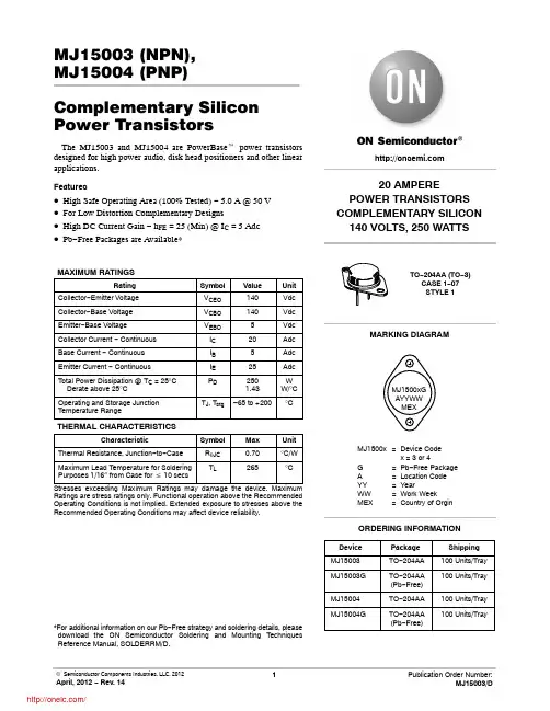
MJ15001;MJ15001G;MJ15002;MJ15002G;中文规格书,Datasheet资料
- 格式:pdf
- 大小:171.12 KB
- 文档页数:5
Symbol
Min
Max
Unit
VCEO(sus) ICEX
ICEO IEBO
140
−
Vdc
−
100 mAdc
−
2.0 mAdc
−
250 mAdc
−
100 mAdc
IS/b
hFE VCE(sat) VBE(on)
Adc
5.0
−
0.5
−
25
150
−
−
1.0
Vdc
−
2.0
Vdc
fT
2.0
−
MHz
Cob
−
Publication Order Number: MJ15001/D
MJ15001 (NPN), MJ15002 (PNP)
ÎÎÎÎÎÎÎÎÎÎÎÎÎÎÎÎÎÎÎÎÎÎÎÎÎÎÎÎÎÎÎÎÎ ELECTRICAL CHARACTERISTICS (TC = 25°C unless otherwise noted) ÎÎÎÎÎÎÎÎÎÎÎÎÎÎÎÎÎÎÎÎÎÎÎÎÎÎÎÎÎÎÎÎÎ Characteristic ÎÎÎÎÎÎÎÎÎÎÎÎÎÎÎÎÎÎÎÎÎÎÎÎÎÎÎÎÎÎÎÎÎ OFF CHARACTERISTICS ÎÎÎÎÎÎÎÎÎÎÎÎÎÎÎÎÎÎÎÎÎÎÎÎÎÎÎÎÎÎÎÎÎ Collector−Emitter Sustaining Voltage (Note 1) ÎÎÎÎÎÎÎÎÎÎÎÎÎÎÎÎÎÎÎÎÎÎÎÎÎÎÎÎÎÎÎÎÎ (IC, = 200 mAdc, IB = 0)
Purposes 1/16″ from Case for v 10 secs
RqJC TL
0.875 265
°C/W °C
ÎÎÎÎÎÎÎÎÎÎÎÎÎÎÎÎÎÎÎ Stresses exceeding Maximum Ratings may damage the device. Maximum ÎÎÎÎÎÎÎÎÎÎÎÎÎÎÎÎÎÎÎ Ratings are stress ratings only. Functional operation above the Recommended
The data of Figure 1 is based on TJ (pk) = 200°C; TC is variable depending on conditions. At high case temperatures, thermal limitations will reduce the power that can be handled to values less than the limitations imposed by second breakdown.
1000
pF
1. Pulse Test: Pulse Width = 300 ms, Duty Cycle v 2%.
IC, COLLECTOR CURRENT (AMP)
200 TC = 25°C
10 7 5 3 2
1
TJ = 200°C BONDING WIRE LIMITED
0.7
THERMAL LIMITATION (SINGLE PULSE)
Shipping 100 Units/Tray
MJ15002G
TO−204AA (Pb−Free)
100 Units/Tray
© Semiconductor Components Industries, LLC, 2011
1
August, 2011 − Rev. 5
/
Operating Conditions is not implied. Extended exposure to stresses above the
Recommended Operating Conditions may affect device reliability.
*For additional information on our Pb−Free strategy and soldering details, please download the ON Semiconductor Soldering and Mounting Techniques Reference Manual, SOLDERRM/D.
There are two limitations on the power handling ability of a transistor: average junction temperature and second breakdown. Safe operating area curves indicate IC − VCE limits of the transistor that must be observed for reliable operation; i.e., the transistor must not be subjected to greater dissipation than the curves indicate.
• These are Pb−Free Devices*
ÎÎÎÎÎÎÎÎÎÎÎÎÎÎÎÎÎÎÎ MAXIMUM RATINGS ÎÎÎÎÎÎÎÎÎÎÎÎÎÎÎÎÎÎÎ Rating
Collector−Emitter Voltage
ÎÎÎÎÎÎÎÎÎÎÎÎÎÎÎÎÎÎÎ Collector−Base Voltage ÎÎÎÎÎÎÎÎÎÎÎÎÎÎÎÎÎÎÎ Emitter−Base Voltage ÎÎÎÎÎÎÎÎÎÎÎÎÎÎÎÎÎÎÎ Collector Current − Continuous ÎÎÎÎÎÎÎÎÎÎÎÎÎÎÎÎÎÎÎ Base Current − Continuous ÎÎÎÎÎÎÎÎÎÎÎÎÎÎÎÎÎÎÎ Emitter Current − Continuous ÎÎÎÎÎÎÎÎÎÎÎÎÎÎÎÎÎÎÎÎÎÎÎÎÎÎÎÎÎÎÎÎÎÎÎÎÎÎ Total Power Dissipation @ TC = 25°C
MJ1500x = Device Code
x = 1 or 2
G
= Pb−Free Package
A
= Location Code
YY
= Year
WW
= Work Week
MEX
= Country of Orgin
ORDERING INFORMATION
Device MJ15001G
Package
TO−204AA (Pb−Free)
Derate above 25°C
Symbol VCEO VCBO VEBO IC IB IE PD
Value 140 140
5 15 5 20 200 1.14
Unit Vdc Vdc Vdc Adc Adc Adc W W/°C
ÎÎÎÎÎÎÎÎÎÎÎÎÎÎÎÎÎÎÎ Operating and Storage Junction ÎÎÎÎÎÎÎÎÎÎÎÎÎÎÎÎÎÎÎ Temperature Range
MJ15001 (NPN), MJ15002 (PNP)
Complementary Silicon Power Transistors
The MJ15001 and MJ15002 are power transistors designed for high power audio, disk head positioners and other linear applications.
TJ, Tstg –65 to +200 °C
ÎÎÎÎÎÎÎÎÎÎÎÎÎÎÎÎÎÎÎ THERMAL CHARACTERISTICS
ÎÎÎÎÎÎÎÎÎÎÎÎÎÎÎÎÎÎÎ Characteristic
பைடு நூலகம்
Symbol
Max
Unit
ÎÎÎÎÎÎÎÎÎÎÎÎÎÎÎÎÎÎÎ Thermal Resistance, Junction−to−Case ÎÎÎÎÎÎÎÎÎÎÎÎÎÎÎÎÎÎÎ Maximum Lead Temperature for Soldering
0.5
SECOND BREAKDOWN LIMITED
0.3
CURVES APPLY BELOW RATED VCEO
0.2 23
5 7 10
20 30 50 70 100 200
VCE, COLLECTOR-EMITTER VOLTAGE (VOLTS)
Figure 1. Active−Region Safe Operating Area
20 AMPERE POWER TRANSISTORS COMPLEMENTARY SILICON 140 VOLTS, 250 WATTS
TO−204AA (TO−3) CASE 1−07 STYLE 1
MARKING DIAGRAM
MJ1500xG AYYWW MEX
(VCE = 100 Vdc, t = 1 s (non−repetitive))
ÎÎÎÎÎÎÎÎÎÎÎÎÎÎÎÎÎÎÎÎÎÎÎÎÎÎÎÎÎÎÎÎÎ ON CHARACTERISTICS ÎÎÎÎÎÎÎÎÎÎÎÎÎÎÎÎÎÎÎÎÎÎÎÎÎÎÎÎÎÎÎÎÎ DC Current Gain ÎÎÎÎÎÎÎÎÎÎÎÎÎÎÎÎÎÎÎÎÎÎÎÎÎÎÎÎÎÎÎÎÎ (IC = 4 Adc, VCE = 2 Vdc) ÎÎÎÎÎÎÎÎÎÎÎÎÎÎÎÎÎÎÎÎÎÎÎÎÎÎÎÎÎÎÎÎÎ Collector−Emitter Saturation Voltage
Features
• High Safe Operating Area (100% Tested) − 5.0 A @ 40 V
0.5 A @ 100 V