组件工艺流程中英文版
- 格式:docx
- 大小:17.81 KB
- 文档页数:4
晶圆制造工艺流程英文版9个步骤The process of semiconductor wafer manufacturing involves several key steps to produce high-quality integrated circuits. The following is a detailed explanation of the nine-stepwafer manufacturing process.Step 1: Wafer SelectionThe first step in the manufacturing process is the selection of high-grade silicon wafers. These wafers are carefully inspected for any defects or impurities that could affect the performance of the integrated circuits.Step 2: CleaningOnce the wafers have been selected, they undergo arigorous cleaning process to remove any residual contaminants. This step is crucial to ensure that the wafers are free from any particles that could interfere with the subsequent manufacturing steps.Step 3: Photoresist CoatingAfter the cleaning process, a photoresist material is coated onto the wafers. This material is sensitive to light and is used to transfer the circuit patterns onto the wafers.Step 4: ExposureThe coated wafers are then exposed to ultraviolet light through a mask that contains the desired circuit patterns. This process transfers the patterns onto the photoresist material, creating a template for the circuitry.Step 5: DevelopmentThe exposed wafers are submerged in a developer solution, which removes the unexposed photoresist material. This step reveals the circuit patterns on the wafers, which will serve as a guide for the subsequent etching process.Step 6: EtchingThe wafers undergo a chemical etching process to remove the exposed silicon material, creating the actual circuit patterns on the surface of the wafers.Step 7: DopingDoping is the process of introducing impurities into the silicon to alter its electrical properties. This step is crucial for creating the necessary components, such as transistors, on the integrated circuits.Step 8: MetallizationOnce the circuit patterns have been defined, a thin layer of metal is deposited onto the surface of the wafers. This metal layer serves as the interconnects for the integrated circuits, allowing for electrical signals to pass between components.Step 9: Testing and PackagingThe final step in the manufacturing process involves testing the completed wafers for quality and functionality. Once the wafers have been tested, they are cut intoindividual chips and packaged for distribution to electronics manufacturers.In conclusion, the semiconductor wafer manufacturing process is a complex series of steps that are carefully orchestrated to produce high-quality integrated circuits. Each step plays a crucial role in defining the circuit patterns and ensuring the functionality of the final product.。
IntroductionThe photovoltaic (PV) industry, an essential component of the global renewable energy landscape, is characterized by its continuous pursuit of high-quality and high-standard manufacturing processes. These processes are critical to ensuring the efficiency, reliability, and longevity of solar modules, which directly impact their overall performance and return on investment. This comprehensive analysis delves into the intricate steps involved in the PV manufacturing process, emphasizing the multi-faceted strategies employed to maintain and enhance product quality and adherence to stringent standards.1. Silicon Feedstock ProcessingThe PV manufacturing process begins with the procurement and refinement of silicon feedstock, the primary raw material for most solar cells. High-quality monocrystalline or multicrystalline silicon is obtained through processes such as the Czochralski (CZ) method or the directional solidification technique. These methods ensure the production of silicon ingots with low impurity levels and optimized crystal structures, vital for maximizing cell efficiency. Rigorous quality control measures, including in-line monitoring and post-processing inspections, are implemented to verify the purity, resistivity, and structural integrity of the silicon.2. Wafer FabricationSilicon ingots are sliced into thin wafers, typically 150-200 micrometers thick, using wire saws or diamond-coated blades. The wafer fabrication stage involves precise control over wafer thickness, flatness, and surface roughness to minimize optical losses and ensure uniformity across the production batch. Advanced texturing techniques, such as alkaline etching or laser doping, are applied to create microstructures on the wafer surface, enhancing light absorption and reducing reflectance. Quality control at this stage includes visual inspections, edge isolation, and electrical testing to identify and weed out defective wafers.3. Solar Cell ProcessingSolar cell processing transforms the silicon wafers into functional devices capable of converting sunlight into electricity. Key steps include:a) Surface Passivation: High-quality dielectric films, such as silicon nitride or aluminum oxide, are deposited on both sides of the wafer to reduce surface recombination and improve minority carrier lifetime, thereby enhancing cell efficiency.b) Diffusion: Phosphorus or boron dopants are introduced into the wafer to form the p-n junction, the heart of the solar cell where photogenerated electrons and holes separate and generate current. Precise control over diffusion temperature, time, and gas concentration is crucial to achieve the desired junction depth and sheet resistance.c) Metallization: Fine-line screen printing or advanced plating techniques are used to deposit metal contacts (usually silver or aluminum) on the front and back surfaces of the cell. The design and layout of these contacts significantly influence cell efficiency by minimizing shading losses and optimizing current collection.d) Anti-Reflection Coating (ARC): A thin layer of silicon nitride or other materials is applied to the front surface of the cell, further reducing surface reflection and enhancing light trapping.Throughout this stage, rigorous quality control measures are in place, including real-time process monitoring, in-line metrology, and periodic sampling for detailed characterization and analysis. These measures ensure compliance with industry standards like IEC 61215 and IEC 61730, which govern the performance, safety, and durability of PV modules.4. Module AssemblyHigh-quality PV modules are assembled from individual cells, encapsulated between ethylene-vinyl acetate (EVA) sheets and protected by a durable glass cover and a weather-resistant backsheet. Stringing the cells in series, soldering interconnects, and laminating the components under vacuum and elevated temperatures ensure electrical connectivity, mechanical stability, andenvironmental protection. Quality control during module assembly encompasses visual inspections, electroluminescence imaging, and flash testing to assess cell-to-cell variations, detect micro-cracks or hotspots, and verify power output and performance parameters.5. Reliability Testing and CertificationTo meet high-standard requirements, PV modules undergo a battery of rigorous reliability tests simulating various environmental and stress conditions they may encounter during their service life. These tests, as outlined in international standards like IEC 61215, IEC 61730, and UL 1703, include thermal cycling, humidity-freeze, damp heat, mechanical load, and potential-induced degradation (PID) tests. Successful completion of these tests earns modules certifications from recognized bodies like TÜV Rheinland, UL, or Intertek, providing assurance of their long-term performance and durability.6. Supply Chain Management and TraceabilityEnsuring high-quality, high-standard PV products also necessitates robust supply chain management and traceability systems. Manufacturers collaborate closely with suppliers to verify the quality and sustainability of raw materials, components, and auxiliary services. Advanced digital platforms enable end-to-end tracking of materials and processes, facilitating quick identification and resolution of quality issues, adherence to international regulations, and fulfillment of customer-specific requirements.ConclusionThe high-quality, high-standard PV manufacturing process is a testament to the industry's commitment to delivering efficient, reliable, and long-lasting solar energy solutions. From the meticulous processing of silicon feedstock to the rigorous testing and certification of finished modules, each stage is infused with a multi-dimensional approach to quality control, technological innovation, and adherence to international standards. As the global shift towards renewable energy accelerates, the ongoing refinement and optimization of this complex process will continue to drive advancements in solar technology, fostering amore sustainable and resilient energy future.。
各位,你们好。
我是方文军。
下边是关于光伏组件的生产工艺,也是我的一点学习心得希望对你们有所帮助。
TEL 183******** QQ 724393030.如果有问题,可以随时联络我。
组件线又叫封装线,封装是太阳能电池生产中的关键步骤,没有良好的封装工艺,多好的电池也生产不出好的组件板。
电池的封装不仅可以使电池的寿命得到保证,而且还增强了电池的抗击强度。
产品的高质量和高寿命是赢得可客户满意的关键,所以组件板的封装质量非常重要。
工艺流程如下:1、电池检测——2、正面焊接—检验—3、背面串接—检验—4、敷设(玻璃清洗、材料切割、玻璃预处理、敷设)——5、层压——6、去毛边(去边、清洗)——7、装边框(涂胶、装角键、冲孔、装框、擦洗余胶)——8、焊接接线盒——9、高压测试——10、组件测试—外观检验—11、包装入库;1.2工艺简介:在这里只简单的介绍一下工艺的作用,给大家一个感性的认识,具体内容后面再详细介绍:1、电池测试:由于电池片制作条件的随机性,生产出来的电池性能不尽相同,所以为了有效的将性能一致或相近的电池组合在一起,所以应根据其性能参数进行分类;电池测试即通过测试电池的输出参数(电流和电压)的大小对其进行分类。
以提高电池的利用率,做出质量合格的电池组件。
2、正面焊接:是将汇流带焊接到电池正面(负极)的主栅线上,汇流带为镀锡的铜带,我们使用的焊接机可以将焊带以多点的形式点焊在主栅线上。
焊接用的热源为一个红外灯(利用红外线的热效应)。
焊带的长度约为电池边长的2倍。
多出的焊带在背面焊接时与后面的电池片的背面电极相连。
(我们公司采用的是手工焊接)3、背面串接:背面焊接是将36片电池串接在一起形成一个组件串,我们目前采用的工艺是手动的,电池的定位主要靠一个膜具板,上面有36个放置电池片的凹槽,槽的大小和电池的大小相对应,槽的位置已经设计好,不同规格的组件使用不同的模板,操作者使用电烙铁和焊锡丝将“前面电池”的正面电极(负极)焊接到“后面电池”的背面电极(正极)上,这样依次将36片串接在一起并在组件串的正负极焊接出引线。
焊接工艺流程译成英文(中英文版)Welding Process Flow: A Comprehensive Translation焊接工艺流程:全面翻译The welding process flow encompasses a series of intricate steps that ensure the fusion of metal parts. It begins with the careful preparation of materials and equipment, followed by the execution of specific welding techniques, and concludes with rigorous inspections to guarantee the integrity of the weld.焊接工艺流程包括一系列确保金属部件融合的复杂步骤。
它从材料与设备的精心准备开始,接着执行特定的焊接技术,并以严格的检查来确保焊接的完整性。
Preparation phase involves cleaning the metal surfaces to remove dirt, oil, and rust, which could compromise the quality of the weld. This is followed by selecting the appropriate welding consumables such as electrodes, filler metals, and shielding gases.准备阶段涉及清洁金属表面,去除可能影响焊接质量的污垢、油污和锈迹。
接下来是选择合适的焊接耗材,如电极、填充金属和屏蔽气体。
In the execution phase, various welding methods such asArc Welding, MIG/MAG Welding, TIG Welding, and Flux-cored Arc Welding are employed based on the material type and thickness. Each method has its unique set of parameters that must be meticulously controlled to achieve optimal results.在执行阶段,根据材料类型和厚度,采用各种焊接方法,如电弧焊、MIG/MAG焊、TIG焊和药芯电弧焊。
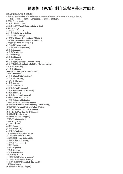
线路板(PCB)制作流程中英⽂对照表线路板(PCB)流程术语中英⽂对照流程简介:开料--钻孔--⼲膜制程--压合--减铜--电镀--塞孔--防焊(绿漆/绿油)--镀⾦--喷锡--成型--开短路测试--终检--雷射钻孔A. 开料( Cut Lamination)a-1 裁板( Sheets Cutting)a-2 原物料发料(Panel)(Shear material to Size)B. 钻孔(Drilling)b-1 内钻(Inner Layer Drilling )b-2 ⼀次孔(Outer Layer Drilling )b-3 ⼆次孔(2nd Drilling)b-4 雷射钻孔(Laser Drilling )(Laser Ablation )b-5 盲(埋)孔钻孔(Blind & Buried Hole Drilling)C. ⼲膜制程( Photo Process(D/F))c-1 前处理(Pretreatment)c-2 压膜(Dry Film Lamination)c-3 曝光(Exposure)c-4 显影(Developing)c-5 蚀铜(Etching)c-6 去膜(Stripping)c-7 初检( Touch-up)c-8 化学前处理,化学研磨( Chemical Milling )c-9 选择性浸⾦压膜(Selective Gold Dry Film Lamination)c-10 显影(Developing )c-11 去膜(Stripping )Developing , Etching & Stripping ( DES )D. 压合Laminationd-1 ⿊化(Black Oxide Treatment)d-2 微蚀(Microetching)d-3 铆钉组合(eyelet )d-4 叠板(Lay up)d-5 压合(Lamination)d-6 后处理(Post Treatment)d-7 ⿊氧化( Black Oxide Removal )d-8 铣靶(spot face)d-9 去溢胶(resin flush removal)E. 减铜(Copper Reduction)e-1 薄化铜(Copper Reduction)F. 电镀(Horizontal Electrolytic Plating)f-1 ⽔平电镀(Horizontal Electro-Plating) (Panel Plating)f-2 锡铅电镀( Tin-Lead Plating ) (Pattern Plating)f-3 低于1 mil ( Less than 1 mil Thickness )f-4 ⾼于1 mil ( More than 1 mil Thickness)f-5 砂带研磨(Belt Sanding)f-6 剥锡铅( Tin-Lead Stripping)f-7 微切⽚( Microsection)G. 塞孔(Plug Hole)g-1 印刷( Ink Print )g-2 预烤(Precure)g-3 表⾯刷磨(Scrub)g-4 后烘烤(Postcure)H. 防焊(绿漆/绿油): (Solder Mask)h-1 C⾯印刷(Printing Top Side)h-2 S⾯印刷(Printing Bottom Side)h-3 静电喷涂(Spray Coating)h-4 前处理(Pretreatment)h-5 预烤(Precure)h-6 曝光(Exposure)h-7 显影(Develop)h-8 后烘烤(Postcure)h-9 UV烘烤(UV Cure)h-10 ⽂字印刷( Printing of Legend )h-11 喷砂( Pumice)(Wet Blasting)h-12 印可剥离防焊(Peelable Solder Mask)I . 镀⾦Gold platingi-1 ⾦⼿指镀镍⾦( Gold Finger )i-2 电镀软⾦(Soft Ni/Au Plating)i-3 浸镍⾦( Immersion Ni/Au) (Electroless Ni/Au)J. 喷锡(Hot Air Solder Leveling)j-1 ⽔平喷锡(Horizontal Hot Air Solder Leveling)j-2 垂直喷锡( Vertical Hot Air Solder Leveling)j-3 超级焊锡(Super Solder )j-4. 印焊锡突点(Solder Bump)K. 成型(Profile)(Form)k-1 捞型(N/C Routing ) (Milling)k-2 模具冲(Punch)k-3 板⾯清洗烘烤(Cleaning & Backing)k-4 V型槽( V-Cut)(V-Scoring)k-5 ⾦⼿指斜边( Beveling of G/F)L. 开短路测试(Electrical Testing) (Continuity & Insulation Testing) l-1 AOI 光学检查( AOI Inspection)l-2 VRS ⽬检(Verified & Repaired)l-3 泛⽤型治具测试(Universal Tester)l-4 专⽤治具测试(Dedicated Tester)l-5 飞针测试(Flying Probe)M. 终检( Final Visual Inspection)m-1 压板翘( Warpage Remove)m-2 X-OUT 印刷(X-Out Marking)m-3 包装及出货(Packing & shipping)m-4 ⽬检( Visual Inspection)m-5 清洗及烘烤( Final Clean & Baking)m-6 护铜剂(ENTEK Cu-106A)(OSP)m-7 离⼦残余量测试(Ionic Contamination Test )(Cleanliness Test) m-8 冷热冲击试验(Thermal cycling Testing)m-9 焊锡性试验( Solderability Testing )N. 雷射钻孔(Laser Ablation)N-1 雷射钻Tooling孔(Laser ablation Tooling Hole)N-2 雷射曝光对位孔(Laser Ablation Registration Hole)N-3 雷射Mask制作(Laser Mask)N-4 雷射钻孔(Laser Ablation)N-5 AOI 检查及VRS ( AOI Inspection & Verified & Repaired)N-6 Blaser AOI (after Desmear and Microetching)N-7 除胶渣(Desmear)N-8 微蚀(Microetching )。

太阳能电池组件生产流程英文解说中文:太阳能电池组件生产工艺组件线又叫封装线,封装是太阳能电池生产中的关键步骤,没有良好的封装工艺,多好的电池也生产不出好的组件板。
电池的封装不仅可以使电池的寿命得到保证,而且还增强了电池的抗击强度。
产品的高质量和高寿命是赢得可客户满意的关键,所以组件板的封装质量非常重要。
工艺流程如下:1、电池检测——2、正面焊接—检验—3、背面串接—检验—4、敷设(玻璃清洗、材料切割、玻璃预处理、敷设)——5、层压——6、去毛边(去边、清洗)——7、装边框(涂胶、装角键、冲孔、装框、擦洗余胶)——8、焊接接线盒——9、高压测试——10、组件测试—外观检验—11、包装入库;1.2工艺简介:在这里只简单的介绍一下工艺的作用,给大家一个感性的认识,具体内容后面再详细介绍:1、电池测试:由于电池片制作条件的随机性,生产出来的电池性能不尽相同,所以为了有效的将性能一致或相近的电池组合在一起,所以应根据其性能参数进行分类;电池测试即通过测试电池的输出参数(电流和电压)的大小对其进行分类。
以提高电池的利用率,做出质量合格的电池组件。
2、正面焊接:是将汇流带焊接到电池正面(负极)的主栅线上,汇流带为镀锡的铜带,我们使用的焊接机可以将焊带以多点的形式点焊在主栅线上。
焊接用的热源为一个红外灯(利用红外线的热效应)。
焊带的长度约为电池边长的2倍。
多出的焊带在背面焊接时与后面的电池片的背面电极相连。
(我们公司采用的是手工焊接)3、背面串接:背面焊接是将36片电池串接在一起形成一个组件串,我们目前采用的工艺是手动的,电池的定位主要靠一个膜具板,上面有36个放置电池片的凹槽,槽的大小和电池的大小相对应,槽的位置已经设计好,不同规格的组件使用不同的模板,操作者使用电烙铁和焊锡丝将“前面电池”的正面电极(负极)焊接到“后面电池”的背面电极(正极)上,这样依次将36片串接在一起并在组件串的正负极焊接出引线。
4、层压敷设:背面串接好且经过检验合格后,将组件串、玻璃和切割好的EVA 、玻璃纤维、背板按照一定的层次敷设好,准备层压。

备料流程步骤说明(中英文实用版)英文文档内容:The material preparation process involves several steps to ensure that all necessary components are ready for production.Here is a detailed explanation of the material preparation process:1.Receiving: The first step in the material preparation process is receiving the raw materials.This involves inspecting the materials to ensure they meet the required specifications and quality standards.2.Sorting: Once the materials have been received and inspected, they need to be sorted based on their type and specifications.This ensures that the correct materials are used for each production task.3.Storage: After sorting, the materials need to be stored in a safe and organized manner.This may involve using racks, bins, or other storage solutions to keep the materials accessible and prevent damage.4.Inventory Management: It is important to keep track of the materials in storage to ensure that they are available when needed.This involves maintaining an accurate inventory database and regularly checking the stock levels.5.Kitting: In some cases, materials may need to be grouped together into kits or assemblies for use in production.This involves gathering all the necessary components and packaging them in a way that makesthem easy to handle and transport.6.Machining and Processing: Some materials may require additional machining or processing before they can be used in production.This may involve cutting, shaping, or drilling the materials to create the desired components.7.Quality Control: Throughout the material preparation process, it is important to perform quality control checks to ensure that the materials meet the required specifications.This may involve inspecting the materials for defects or using testing equipment to verify their properties.8.Delivery: Once the materials have been prepared and inspected, they need to be delivered to the production floor or to the appropriate workstations.This may involve using material handling equipment or transporting the materials by hand.Overall, the material preparation process is crucial to ensuring that all necessary components are ready for production.By following these steps and maintaining accurate records, businesses can streamline their production processes and improve overall efficiency.中文文档内容:物料准备工作涉及多个步骤,以确保所有必要的组件都已准备好生产。
pcb插件工艺流程英文English Answer:PCB Assembly Process.The PCB assembly process is a complex and multi-step one that involves a number of different steps, including:1. Design and layout: The first step in the PCB assembly process is to design and layout the board. This involves creating a schematic diagram of the circuit, as well as a layout for the board itself. The layout of the board will determine the placement of the components on the board, as well as the routing of the traces.2. Fabrication: Once the design and layout of the board have been finalized, the board is fabricated. This involves creating the physical board itself, as well as the traces and other features on the board. The fabrication process typically involves a number of steps, including:Laminating: The first step in the fabrication process is to laminate the board. This involves bonding together multiple layers of material to create the board itself. The layers of material typically include a copper layer, a core layer, and a solder mask layer.Drilling: Once the board has been laminated, the next step is to drill the holes for the components. The holes are typically drilled using a CNC (computer numerical control) machine.Plating: After the holes have been drilled, the board is plated. This involves coating the board with athin layer of metal, such as copper or gold. The plating process helps to protect the board from corrosion and wear.Soldering: The final step in the fabrication process is to solder the components to the board. This involves melting solder and applying it to the joints between the components and the board. The soldering process is typically done using a wave soldering machine.3. Testing: Once the board has been assembled, it is tested to ensure that it is functioning properly. This involves testing the board for a variety of parameters,such as electrical continuity, shorts, and opens. Thetesting process typically involves using a variety of test equipment, such as a multimeter and an oscilloscope.4. Inspection: After the board has been tested, it is inspected to ensure that it meets all of the specifications. This involves visually inspecting the board for any defects, as well as measuring the board to ensure that it is within the specified tolerances.5. Packaging and shipping: Once the board has been inspected and approved, it is packaged and shipped to the customer. The packaging process typically involves placing the board in a protective box or container, as well as labeling the board with the necessary information, such as the part number and the serial number.Chinese Answer:PCB插件工艺流程。
晶圆制造工艺流程英文版9个步骤The manufacturing process of semiconductor wafers involves several crucial steps to produce high-quality chips. The following nine steps outline the typical process used in semiconductor wafer manufacturing:Step 1: Wafer Ingot GrowthThe process begins with the growth of a silicon ingot, which serves as the starting material for the wafers. The ingot is carefully grown using the Czochralski method, where a seed crystal is dipped into molten silicon and slowly drawn out to form a cylindrical ingot.Step 2: Ingot CuttingOnce the ingot has been grown to the desired size, it is then cut into thin wafers using a diamond wire saw. This step requires precision to ensure the wafers are of uniform thickness and free from defects.Step 3: Surface PolishingAfter cutting, the wafers undergo a series of chemical and mechanical processes to remove any surface imperfections and create a mirror-like finish. This step is critical to ensure the wafers are pristine and ready for the next stages of processing.Step 4: PhotolithographyIn this step, a light-sensitive photoresist is coated onto the wafer's surface, followed by exposure to UV light through a photomask. This process transfers the pattern of the photomask onto the wafer, defining the circuit layout for the chips.Step 5: EtchingThe exposed areas of the wafer are selectively etched away using chemical or plasma etching processes, leavingbehind the desired pattern in the wafer. This step is crucial for defining the circuitry and features of the chips.Step 6: DopingDopants such as phosphorus or boron are implanted into the wafer to modify its electrical properties and create the necessary regions for transistor formation. This step is essential for controlling the conductivity of the semiconductor material.Step 7: Thermal ProcessingThe doped wafers undergo high-temperature annealing processes to activate the dopants and repair any damage caused during doping and etching. This step is critical for ensuring the proper functioning of the semiconductor devices.Step 8: MetallizationThin films of metal are deposited onto the wafer's surface to create interconnections and contacts for thesemiconductor devices. This step involves sputtering or evaporation of metal layers followed by patterning through photolithography and etching.Step 9: PackagingThe individual wafers are diced into separate chips and assembled into packages, along with wire bonding and encapsulation processes to protect the chips. This final step prepares the chips for testing and integration intoelectronic devices.In conclusion, the manufacturing process of semiconductor wafers involves a series of intricate steps, each of which plays a crucial role in producing high-performance chips for electronic applications. From ingot growth to packaging, careful control and precision are essential to ensure the quality and reliability of the semiconductor devices.。
组件工序流程介绍英文English:The process flow of component manufacturing involves several key steps. First, it starts with material preparation, where raw materials are gathered and inspected for quality. Next, comes the machining process, where the material is shaped and formed according to the design specifications using various tools such as lathes, mills, and drills. Following machining, there's the assembly phase, where individual components are put together to create the final product. This often involves welding, soldering, or adhesive bonding depending on the materials used. After assembly, the components undergo testing to ensure they meet quality standards and function as intended. This includes both dimensional checks and functional tests to verify performance. Finally, the finished components are packaged and prepared for shipping to customers.Translated content:零部件制造的工序流程涉及几个关键步骤。
太阳能板工艺流程英语Here's a sample of a conversational and informal English text describing the process of manufacturing solar panels, with each paragraph maintaining independence in style and language:Alright, let's dive into the basics of how solar panels are made. It all starts with the raw materials — silicon wafers, mostly. These wafers are cut into thin slices, just like slicing a pizza, but precision is key.After slicing, the wafers go through a cleaning process to remove any impurities. Think of it like giving your phone a good scrub before putting on a new case. Cleanliness is essential for efficiency.Next up, these wafers are coated with photovoltaic cells. It's like painting a canvas, but with science! These cells are what convert sunlight into electricity.Once the cells are in place, it's time for assembly. The wafers are encased in a protective frame and glass cover. This step is crucial for durability and long-term use.And finally, the solar panels undergo rigorous testing. They're exposed to various conditions to ensure they can stand up to the real world. It's like a solar panel boot camp!。
十层电路板工艺流程英语Ten-Layer PCB Fabrication Process.The fabrication of a ten-layer printed circuit board (PCB) involves a series of complex and precise steps that require specialized equipment and materials. The process typically begins with the design of the PCB layout, whichis then transferred to a physical board using a variety of techniques. The board is then processed through a series of chemical, mechanical, and electrical steps to create the desired circuit pattern and electrical connections.1. Design.The first step in the PCB fabrication process is to design the layout of the board. This is typically done using a computer-aided design (CAD) software program, which allows the designer to create a precise representation of the board's electrical connections and physical dimensions. The CAD file is then used to generate a set ofmanufacturing instructions that will be used to create the physical board.2. Fabrication.Once the design is complete, the PCB is fabricated using a variety of techniques. The most common method is to use a subtractive process, in which a copper-clad laminate is etched to create the desired circuit pattern. This process begins by applying a photoresist layer to the laminate, which is then exposed to ultraviolet light through a mask that defines the circuit pattern. The exposed areas of the photoresist are then developed, leaving the copper exposed in the areas that will form the circuit traces. The board is then etched in a chemical solution that removes the exposed copper, leaving the desired circuit pattern.3. Drilling.Once the circuit pattern is created, holes are drilled into the board to allow for the insertion of components.The holes are typically drilled using a CNC machine, which uses a computer-controlled drill to precisely locate and drill the holes. The size and location of the holes are determined by the design of the board.4. Plating.After the holes are drilled, the board is plated with a thin layer of copper to protect the copper traces and to provide a surface for soldering. The plating process is typically done using an electroless deposition process, in which the copper is deposited onto the board using a chemical reaction.5. Laminating.The next step in the PCB fabrication process is to laminate the board to a layer of insulating material. This is typically done using a press that applies heat and pressure to bond the two layers together. The insulating material is typically made of a fiberglass-reinforced epoxy resin, which provides strength and electrical insulation.6. Pressing.After the board is laminated, it is pressed to create a smooth and flat surface. This is typically done using a hydraulic press, which applies a uniform pressure to the board. The pressing process also helps to remove any air bubbles that may have been trapped between the layers of the board.7. Routing.Once the board is pressed, it is routed to create the final shape and size. This is typically done using a CNC router, which uses a computer-controlled cutting tool to cut the board to the desired shape. The routing process also creates any slots or cutouts that may be required for the board to fit into its enclosure.8. Testing.After the board is routed, it is tested to ensure thatit meets the design specifications. This is typically done using a variety of electrical tests, which check for continuity, shorts, and other electrical faults. The board may also be subjected to environmental testing, such as temperature cycling and vibration testing, to ensure that it will withstand the conditions in which it will be used.9. Assembly.Once the board has passed testing, it is ready for assembly. This involves soldering the components to the board, which is typically done using a surface mount technology (SMT) machine. The SMT machine places the components on the board and solders them in place using a reflow oven.10. Inspection.After the board is assembled, it is inspected to ensure that all of the components have been placed correctly and that there are no soldering defects. This is typically done using a combination of visual inspection and automatedoptical inspection (AOI). The AOI machine uses a camera to inspect the board for any defects, such as missing components or solder bridges.The process of fabricating a ten-layer PCB is complex and requires a high level of precision and expertise. By following the steps outlined above, manufacturers can produce high-quality PCBs that meet the demanding requirements of modern electronic devices.。
英文回答:The CSPV process is a key link in the photovoltaic industry and is directly related to the development of our energy industry and the sustainable development of our national economy. This process includes, inter alia, the preparation of crystal silicon materials, the processing of crystal silicon materials, battery tablets, the manufacture of photovoltaicponents and detection. During the preparation phase of the crystal silicon material, the process of selecting, cleaning and cutting the material at customs must be strictly enforced to ensure the quality and purity of the material. It is processed through crystal silicon materials and obtained through processes such as acid washing and polishing. During the battery plate production phase, processes such as optical carving, diffusion, sedimentation metals, etc., must be carried out in accordance with national standards and regulations to make batteries with PN structures. During the manufacturing phase of the photovoltaicponents, it is necessary to ensure the containment mass of the battery plate and to form the photovoltaicponents. Finally, photovoltaicponents are tested to ensure that their quality and performance meet national policies and standards. The healthy and sustainable development of the photovoltaic industry canbe promoted only if national policies and standards are strictly enforced and technological innovation and quality management are strengthened.晶硅光伏组件制作工艺流程是光伏产业的关键环节,直接关系到我国能源产业的发展和国民经济的可持续发展。
中文:太阳能电池组件生产工艺组件线又叫封装线,封装是太阳能电池生产中的关键步骤,没有良好的封装工艺,多好的电池也生产不出好的组件板。
电池的封装不仅可以使电池的寿命得到保证,而且还增强了电池的抗击强度。
产品的高质量和高寿命是赢得可客户满意的关键,所以组件板的封装质量非常重要。
工艺流程如下:1、电池检测——2、正面焊接—检验—3、背面串接—检验—4、敷设(玻璃清洗、材料切割、玻璃预处理、敷设)——5、层压——6、去毛边(去边、清洗)——7、装边框(涂胶、装角键、冲孔、装框、擦洗余胶)——8、焊接接线盒——9、高压测试——10、组件测试—外观检验—11、包装入库;1.2工艺简介:在这里只简单的介绍一下工艺的作用,给大家一个感性的认识,具体内容后面再详细介绍:1、电池测试:由于电池片制作条件的随机性,生产出来的电池性能不尽相同,所以为了有效的将性能一致或相近的电池组合在一起,所以应根据其性能参数进行分类;电池测试即通过测试电池的输出参数(电流和电压)的大小对其进行分类。
以提高电池的利用率,做出质量合格的电池组件。
2、正面焊接:是将汇流带焊接到电池正面(负极)的主栅线上,汇流带为镀锡的铜带,我们使用的焊接机可以将焊带以多点的形式点焊在主栅线上。
焊接用的热源为一个红外灯(利用红外线的热效应)。
焊带的长度约为电池边长的2倍。
多出的焊带在背面焊接时与后面的电池片的背面电极相连。
(我们公司采用的是手工焊接)3、背面串接:背面焊接是将36片电池串接在一起形成一个组件串,我们目前采用的工艺是手动的,电池的定位主要靠一个膜具板,上面有36个放置电池片的凹槽,槽的大小和电池的大小相对应,槽的位置已经设计好,不同规格的组件使用不同的模板,操作者使用电烙铁和焊锡丝将“前面电池”的正面电极(负极)焊接到“后面电池”的背面电极(正极)上,这样依次将36片串接在一起并在组件串的正负极焊接出引线。
4、层压敷设:背面串接好且经过检验合格后,将组件串、玻璃和切割好的EVA 、玻璃纤维、背板按照一定的层次敷设好,准备层压。
玻璃事先涂一层试剂(primer)以增加玻璃和EVA的粘接强度。
敷设时保证电池串与玻璃等材料的相对位置,调整好电池间的距离,为层压打好基础。
(敷设层次:由下向上:玻璃、EVA、电池、EVA、玻璃纤维、背板)。
5、组件层压:将敷设好的电池放入层压机内,通过抽真空将组件内的空气抽出,然后加热使EVA熔化将电池、玻璃和背板粘接在一起;最后冷却取出组件。
层压工艺是组件生产的关键一步,层压温度层压时间根据EVA的性质决定。
我们使用快速固化EVA时,层压循环时间约为25分钟。
固化温度为150℃。
6、修边:层压时EVA熔化后由于压力而向外延伸固化形成毛边,所以层压完毕应将其切除。
7、装框:类似与给玻璃装一个镜框;给玻璃组件装铝框,增加组件的强度,进一步的密封电池组件,延长电池的使用寿命。
边框和玻璃组件的缝隙用硅酮树脂填充。
各边框间用角键连接。
8、焊接接线盒:在组件背面引线处焊接一个盒子,以利于电池与其他设备或电池间的连接。
9、高压测试:高压测试是指在组件边框和电极引线间施加一定的电压,测试组件的耐压性和绝缘强度,以保证组件在恶劣的自然条件(雷击等)下不被损坏。
10、组件测试:测试的目的是对电池的输出功率进行标定,测试其输出特性,确定组件的质量等级。
英文:Solar cell module production processLine called packaging line components, packaging is the production of solar cells a key step in the packaging process without a good, multi-well battery is also not a good component of production boards. Battery package not only the battery life is guaranteed, but also to enhance the combat strength of the battery. Product quality and high service life is to win can be the key to customer satisfaction, so the quality of components of the package board is very important.Process is as follows:1, the battery test - 2, positive Welding - Inspection -3, on the back of cascading - Inspection -4, laying (glass cleaning, material cutting, glasspre-processing, laying) - 5, laminating - 6, to flash ( to the side, cleaning) - 7, fitted border (glue, loading angle keys, punching, install box, scrub I glue) - 8, the welding junction box - 9, high-pressure test - 10, component testing -- -11 appearance inspection, packaging and storage;1.2 Process Description:Here only a brief look at the role of technology, give us an emotional understanding of the specific content of a further detail later:1, the battery test: Because the randomness of the battery-chip manufacturing conditions, the production out of battery performance is different, we will be for the effective performance of identical or similar battery together, it should be classified according to their performance parameters; battery test that is by testing the battery output parameters (current and voltage) of the size of its classification. To improve the utilization of the battery to make the battery components of acceptable quality.2, positive welding: It's convergence with soldered to the battery positive (negative) of the main gate line, convergence zone for the tinned copper strip, we use a welding machine can weld with a multi-point in the form of spotwelding on the main gate Online. Welding heat source for an infrared lamp (using infrared thermal effect). Welding with the length of the side length of about 2 times the battery. More welding belt behind the back of welding with electrodes connected to the back of the battery piece. (Our company uses a manual welding)3, on the back of concatenation: back of the weld is 36 cells cascaded together to form a component of the string, we are currently used process is manual, the battery depends mainly on the positioning of a membrane with plate 36 placed above the battery film grooves, groove size and battery size correspond to the location of tank has been designed well, different specifications of the components use a different template, the operator use electric soldering iron and solder wire will "in front of the battery," the positive electrode (cathode) Welding to the "behind the battery" on the back electrode (cathode), so that in turn will be 36 series with the component string together and welded out of positive and negative leads.4, laminated lay: on the back of a good tandem and tested after passing the component string, glass and cut a good EVA, glass fiber, backplane according to a certain level, laying a good preparation for lamination. Glass pre-coated layer of reagent (primer) in order to increase the bonding strength of glass and EVA. When installed to ensure the battery strings and glass and other materials relative position, adjusting the distance between the battery, in order to laminate lay a solid foundation. (Laying of levels: from the bottom up: glass, EVA, cell, EVA, glass fiber, backplane).5, component lamination: a good battery will be laid into the laminating machine, through the vacuum component of the air out, and then heated to melt the EVA batteries, glass and back bonding together; the final cooling out components. Lamination process is a key step in component production, lamination temperature lamination time, according to the nature of EVA. We use the fast-curing EVA, the lamination cycle time is about 25 minutes. Curing temperature of 150 ℃.6, trimming: laminated EVA melt when the pressure of reaching out after curing due to the formation of flash, so it should be removed laminated finish.7, fitted box: similar to the glass mounted to a frame; to the glass component mounted aluminum frame to increase the intensity of the component, further sealing the battery components, longer battery life. Borders and glass components of the gap filled with silicone resin. The border between the connection with the angle button.8, the welding junction box: In the component lead at the back of a box welded to facilitate the battery and other equipment or connections between cells.9, high-pressure test: high-pressure test is defined as components of the border and the electrode lead a certain voltage is applied between the test component of the pressure resistance and dielectric strength to ensure that components in harsh natural conditions (lightning, etc.) will not be damaged under the .10, component testing: the test objective is to calibrate the battery output power to test its output characteristics, determine the quality grade components。