PMBT4401,215;PMBT4401,235;中文规格书,Datasheet资料
- 格式:pdf
- 大小:88.91 KB
- 文档页数:8

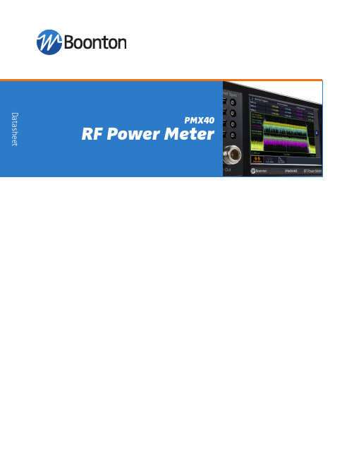
The PMX40 provides design engineers and technicians the utility of traditional benchtop instrument, the flexibility and performance of modern USB RF power sensors, and the simplicity of a multi-touch display built with Boonton award-winning technology.As a benchtop meter, the PMX40 provides a standalone solution for capturing, displaying, and analyzing peak and average RF power in both the time and statistical domains through an intuitive, multi-touch touchscreen display.The PMX40 Power Meter utilizes up to four RTP and CPS families of USB RF power sensors with industry- leading performance and capabilities either independently or for synchronized multi-channel measurements of CW, modulated, and pulsed signals.Providing the ultimate flexibility, the PMX40 sensors can be disconnected and independently used as standalone instruments.Key Features• Capture/display/analyze peak and average power• Frequency range from 4 kHz to 40 GHz• Industry-leading video bandwidth (195 MHz) and rise time (3 ns)• Industry-leading 100,000 measurements per second• Industry-leading 100 ps time resolution• Synchronous multi-channel measurements (up to 4 channels)• Sensors can be used as standalone instruments PMX40 RF Power MeterPulsed ModeAnalysis of fast-rising single pulses or pulses with short pulserepetition intervals (PRIs) requires an instrument with sophisticated trigger and data acquisition capability. Within Pulsed Mode, more than 16 pulse parameters can be measured.Continuous ModeFor simple, intuitive measurements of repetitive waveforms, the PMX40 Continuous Mode of operation provides a numeric display of average, maximum and minimum signal powers.Statistical ModeIn Statistical Mode, the PMX40 plots the Complementary Cumulative Distribution Function (CCDF). The CCDF plot shows the rate of occurrence of a specific crest factor for signals, such as those used in 5G, 4G/LTE, and Wi-Fi applications.PMX40 RF Power Meter – Front PanelConnect up to 4 USB sensors for multi-channel measurements.Multi-touch display with intuitive user interface.One touch to quickly access presets and favorite functions.Sync ports to source or receive triggers for timing and synchronization.Test source to verify sensor operation.The PMX40’s intuitive, multi-touch display enables fast configuration of up to four sensors as well as easy access to measurement and analysis tools, providing a standalone solution for capturing, displaying, and analyzing peak and average RF power in both the time and statistical domains. The meter also incorporates a test source to verify sensor operation.High-Performance and Versatile USB Power Sensors• Real-Time Power Processing™ technology with virtually zero measurement latency • 100,000 measurements per second • 80 dB dynamic range• Synchronized multi-channel measurementsAll RTP Real-Time Power SensorsThe Boonton PMX40 Power Meter utilizes Boonton RTP and CPS families of USB RF power sensors with indus-try leading performance and capabilities. All RTP sensors incorporate the unique Boonton Real-Time Power Processing™ technology, which virtually eliminates gaps in measurement suffered by other power sensors and enables industry best measurement speeds. In terms of RF performance, the RTP5000 series Real-Time Peak Power Sensors are the fastest responding sensors with 3 ns rise times and 195 MHz of video bandwidth. The RTP4000 series Real-Time True Average Power Sensors enable the lowest frequency measurements for diode-based average power measuring sensors and can make accurate measurements virtually independent of signal modulation bandwidth. CPS sensors offer flexible connectivity and performance leadership at anexcellent price point.Real-Time Power Processing™Boonton Real-Time Power Processing 1 dramatically reduces the total cycle time for acquiring and processing power measurement samples. By combining a dedicated acquisition engine, hardware trigger, integrated sample buffer, and a real-time optimized parallel processing architecture, Real-Time Power Processing™ performs most of the sweep processing steps simultaneously, beginning immediately after the trigger instead of waiting for the end of the acquisition cycle.The advantages of the Real-Time Power Processing technique are that key processing steps take place in parallel and keep pace with the signal acquisition. With no added computational overhead to prolong the sweep cycle, the sample buffer cannot overflow. As a result, there is no need to halt acquisition for trace processing. This means gap-free signal acquisition virtually guarantees that intermittent signal phenomena such as transients or dropouts will be reliably captured and analyzed.1RTPP is available within the RTP500 and RTP4000 sensors.Software FeaturesMeasurement Buffer ModeThe RTP series Measurement Buffer Mode is a remote control function that works in conjunction with Real-Time Power Processing to provide only therelevant burst or pulse information, eliminating the need to download and post-process large sample buffers. As a result, users can collect and analyze measurements from a virtually unlimited number of consecutive pulses or events without gaps. A wide variety of parameters can be calculated and plotted, such as duty cycle, pulse repetition rate, pulse width variation, and pulse jitter. In addition, anomalies,such as dropouts, can be identified.Dropouts, such as those shown left, are the sorts of events often missed by conventional power meters due to the acquisition gaps while processing takes place.Example seven pulse waveform.Measurement buffer data returned for waveform in above.Wi-Fi and Wireless Communication Signal AnalysisCharacterization and compliance testing of Wi-Fi and LTE chipsets and devices involves significant challenges for design and test engineers. With multiple-input, multiple-output (MIMO) architectures and channel bandwidths up to 160 MHz, testing is complex, especially when measuring RF power per channel and time alignment between channels. The PMX40 enables packet power measurements to be performed independently on multiple synchronous or asynchronous transmit chains with a common timebase shared among sensors.Use markers to define a portion of the waveform on which to make measurements. “Between Marker” measurements are ideal for monitoring specific portions of a packet over long intervals.Video bandwidth (VBW) describes the ability of a power sensor to track peak (envelope) power. Insufficient VBW will result in errant envelope and average power measurements. The PMX40 offers the widest video bandwidth (195 MHz) making it ideal for measuring 80 MHz, 100 MHz, and 160MHz channels.By comparing the peak-to-average power ratio, or crest factor (CF), of input and output signals of an RF transmission chain, engineers can assess circuit linearity. Additional insight can be provided with the PMX40 statistical mode Complementary Cumulative Distribution Function (CCDF) plot displaying the rate of occurrence of a specific CF. As an amplifier output compresses, the CF will reduce and the CCDF plot will move left.Indication of amplifier output compressionCrest FactorSecondary Surveillance Radar (SSR)Design, verification, troubleshooting and maintenance of secondary surveillanceradar (e.g. IFF-based radar) has never been more demanding.Proper design and operation of SSR systems is critical to the safety and security of aviation. The PMX40 can b e u sed t o easily a nd accurately capture SSR waveforms. Markers enable measurements on specific portions of the waveform.Industry-leading rise time (<3 ns) enables characterization of the most demanding radar signals.Utilize the superior 100 ps time resolution to zoom and uncover signal characteristics that might otherwise be missed.Key Features and Functionality• Data displayed as numerical meter or waveform trace • Statistical analysis with CCDF plot• Multiple marker measurements, including between marker data and marker ratios • Automated measurements; e.g., 16 automated pulse measurements • Export measurement data in .csv or .pdf formats • Up to 8 simultaneous power measurement channels• Simulation mode available to preview functionality when a sensor is not availableKey Features and Functionality• Large numeric readout and/or analog meter display • Zoom and pan through data logging strip chart• Quickly set frequency, aperture (averaging) and offset values all from the main screen• Calculates ratios between sensor measurements • Control up to 8 sensors at once• Simulation mode available to preview functionality when a sensor is not availableSensor SoftwarePower Viewer – Simple and Intuitive Measurement Software(for standalone operation of the CPS2000 Series of sensors)Power Viewer is a complimentary PC-based software package for CPS2008 sensor control, measurement configuration, and analysis. It includes USB drivers, remote control API, firmware updater and virtual instrument application.(for standalone operation of the RTP4000 and RTP5000 series of sensors)Power Analyzer is a complimentary PC-Based software package for RTP5000 and RTP4000 sensor control, measurement configuration, and advanced analysis. It includes USB drivers, remote control API, firmwareupdater and virtual instrument application.Power Analyzer - Advanced Measurement and Analysis SoftwareSensor SpecificationsRTP5006RTP5318 RF Frequency Range50 MHz to 6 GHz50 MHz to 18 GHz Dynamic RangeSpecificationsChannels Up to 4 Sensors RTP5000 SeriesRTP4000 SeriesCPS2000 Series Display5-inch WVGA multi-touch display with intuitive graphical user interfaceDisplay Modes Trace (power vs time)Statistical measurements Meter (numeric display)CCDFAutomatic measurements (pulse, statistical, and markers measurements)Marker Measurements (in Trace View)Markers (vertical cursors)Marker IndependentlyInterval Between MarkersPair of MarkersSettable in time relative to the trigger positionAvg, Min and Max Power at a specified time offsetAvg, Min and Max Power over the defined intervalRatio of power values at each markerPulse Mode – Automatic Measurements Pulse rise-timePulse widthPulse periodPulse duty cyclePulse peakPulse overshootTop level powerEdge delayPulse fall-timePulse off-timePulse repetition frequencyWaveform averagePulse averagePulse droopBottom level powerPulse edge skew between channelsStatistical Mode –Automatic Measurements Peak powerMinimum powerDynamic rangeCrest factor at cursorAverage powerPeak to average ratioPercent at cursorCrest factor at various percentsTrigger Synchronization*ModeSourceInternal Level RangeExternal Level RangeSlopeHold-off, Min Pulse Width, Max Trigger RateAmong RTP Series(internal trig distribution)Normal, Auto, Auto Pk-to-Pk, Free Run Any connected RTP Series sensor (via SMB’s) or rearpanel external trigger -40 dBm to +20 dBm (sensor dependent)±5 volts or TTL+ or -Sensor and timebase dependentTime Base Time Base Resolution, Range, AccuracyTime Base DisplayTrigger Delay RangeTrigger Delay ResolutionSensor dependent Sweeping or Roll Mode Sensor dependent0.02 divisionsSpecifications, ContinuedInputs/Outputs (front panel)USB with SMB trigger port Test Source50 MHz(optional rear panel placement)Inputs/Outputs (rear panel)LANUSB with SMB trigger portWireless Telecom Group Inc. 25 Eastmans Rd Parsippany, NJ United StatesTel: +1 973 386 9696 Fax: +1 973 386 9191 © Copyright 2020 All rights reserved.B/PMX40/0520/ENNote: Specifications, terms and conditions are subject to change without prior notice.PMX40RF Power Meter (includes 2 active channels)OptionsPMX40-4CH PMX40-GPIB PMX40-RTSAdds 2 Active Channels (for a total of 4)GPIB Control (internally installed)Moves Test Source output to the rear panelIncluded AccessoriesInformation Card (provides information on where to download the latest manual, software, utilities)Optional AccessoriesPMX40-RMK PMX40-TCASEFull-width 19” Rack Mount Kit (includes handles & hardware for mounting one or two meters)Transit case, hold the PMX40 and up to 4 sensorsRF Power SensorsCPS2008RTP4006RTP4106RTP4018*RTP4040*RTP5006RTP5318RTP5518RTP5340RTP5540True Average Connected Power Sensor Real-Time True Average Power Sensor Real-Time True Average Power Sensor Real-Time True Average Power Sensor Real-Time True Average Power Sensor Real-Time Peak Power Sensor Real-Time Peak Power Sensor Real-Time Peak Power Sensor Real-Time Peak Power Sensor Real-Time Peak Power Sensor50 MHz to 8 GHz 10 MHz to 6 GHz 4 kHz to 6 GHz 10 MHz to 18 GHz 10 MHz to 40 GHz 50 MHz to 6 GHz 50 MHz to 18 GHz 50 MHz to 18 GHz 50 MHz to 40 GHz 50 MHz to 40 GHzIncluded AccessoriesInformation Card (provides information on where to download the latest manual, software, utilities)0.9 m BNC (m) to SMB (m) cable (RTP sensors)0.9 m SMB (m) to SMB (m) cable (RTP sensors)1.8 m USB A (m) to USB B (m) locking SeaLATCH cable (RTP sensors)1.6 m USB A (m) to USB B (m) cable (CPS sensors)Ordering Information*RTP4018 and RTP4040 are currently in development. Specifications and performance subject to change。

PM140产品说明书概述Firstack数字智能型IGBT驱动是为大功率、高电压IGBT专门开发的,具有功能强大,可靠性高等特点,适用于两电平变流器,其应用覆盖新能源、轨道交通、工业传动及智能电网等各个领域。
PM140驱动产品是以Firstack数字智能型IGBT驱动为基础,针对PrimePACKTM 模块开发的即插即用型驱动。
图1 产品照片目录概述 (1)系统框架图 (3)使用步骤及注意事项 (4)机械尺寸图 (5)引脚定义 (6)状态指示灯说明 (8)驱动参数 (9)主要功能说明 (12)◆短路保护 (12)◆欠压保护 (12)◆软关断 (13)◆温度保护及采样 (13)门极电阻位置指示 (17)订购信息 (19)技术支持 (19)法律免责声明 (19)联系方式 (19)系统框架图数字控制核1D Z1V CC1V EE1软关断电路信号输入1C1级G1级V CC1E1级数字控制核2D Z2V CC2V EE2软关断电路信号输入2C2级G2级V CC2E2级COM1COM2故障指示==V CC1V EE1COM1故障指示电源输入V CE 检测电源检测V CE 检测电源检测故障返回电源V CC2V EE2COM2图2 系统框架图使用步骤及注意事项驱动器简便使用的相关步骤如下:1. 选择合适的驱动器使用驱动器时,应注意该驱动器适配的IGBT模块型号。
对于非指定IGBT 模块无效,使用不当可能会导致驱动和模块失效。
2. 将驱动器安装到IGBT 模块上对IGBT模块或驱动器的任何处理都应遵循国际标准IEC 60747-1第Ⅸ章或欧洲标准EN 100015要求的静电敏感器件保护的一般规范(即工作场所、工具等必须符合这些标准)。
如果忽视这些规范,IGBT和驱动器都可能会损坏。
3. 将驱动器连接到控制单元将驱动器接插件(光纤)连接到控制单元,并为驱动器提供合适的供电电压4. 检查驱动器功能检查门极电压:对于关断状态,额定门极电压在相应的数据手册中给出,对于导通状态,该电压为15V。

DSENSOR数字式通用颗粒物浓度传感器PMS5XXXST系列数据手册主要特性◆激光散射原理实现精准测量◆零错误报警率◆实时响应并支持连续采集◆最小分辨粒径0.3μm◆全新专利结构,六面全方位屏蔽,抗干扰性能更强◆进出风口方向可选,适用范围广,用户无需再进行风道设计◆可实时输出甲醛监测数据◆可实时输出温度及湿度数据概述PMS5XXXST系列是一款可以同时监测空气中颗粒物浓度、甲醛浓度及温湿度的三合一传感器。
其中颗粒物浓度的监测基于激光散射原理,可连续采集并计算单位体积内空气中不同粒径的悬浮颗粒物个数,即颗粒物浓度分布,进而换算成为质量浓度。
甲醛浓度的监测基于电化学原理,具有高精度、高稳定性的特点。
传感器同时内嵌瑞士生产的温湿度一体检测芯片。
颗粒物浓度数值、甲醛浓度数值及温度、湿度合并以通用数字接口形式输出。
本传感器可嵌入各种与空气质量监测和改善相关的仪器设备,为其提供及时准确的环境参数。
工作原理本传感器采用激光散射原理。
即令激光照射在空气中的悬浮颗粒物上产生散射,同时在某一特定角度收集散射光,得到散射光强随时间变化的曲线。
进而微处理器利用基于米氏(MIE)理论的算法,得出颗粒物的等效粒径及单位体积内不同粒径的颗粒物数量。
传感器各功能部分框图如图1所示图1 传感器功能框图甲醛监测功能采用电化学原理实现,加入数据处理算法,所获得的数据稳定、精确。
技术指标如表1所示表1 传感器技术指标数字接口定义PIN1图2 接口示意图输出结果1.颗粒物浓度:主要输出为单位体积内各浓度颗粒物质量以及个数,其中颗粒物个数的单位体积为0.1升,质量浓度单位为:微克/立方米(μg/m³)。
此外传感输出分为主动输出和被动输出两种状态。
传感器上电后默认状态为主动输出,即传感器主动向主机发送串行数据,时间间隔为200~800ms,空气中颗粒物浓度越高,时间间隔越短。
主动输出又分为两种模式:平稳模式和快速模式。
在空气中颗粒物浓度变化较小时,传感器输出为平稳模式,即每三次输出同样的一组数值,实际数据更新周期约为2s。

开关电源驱动模块(PM40XXA)图1是为大功率开关电源设计的专业驱动模块,模块型号定义为:PM4020A和PM4060A两种,PM4020A最大驱动为(以MOS 管为例25A;MOS管)在应用驱动最老的MOS管是IRFP460内部电容大约6000P。
图2是PM4060A最大驱动能力为60A的MOS管或者IGBT管,两个电路图相同、不同的是所使用的驱动IC有区别,前面是使用的IR2101驱动IC、后面是使用IR2181驱动IC,两个驱动电路的脚列完全相同!可以直接代替使用。
上面两种模块的全部技术资料由(老铎)设计!所有出版在“电子制作网”上面。
并且由本网站提供完整的成品(如上图片)。
PM4020A每块30元;PM4060A每块 35元;具体订购方法请参考最后页。
采用该模块设计一个大功率1000W的开关电源是十分简单的事情,你不必花费更多的时间就可以完成,下面的设计是一个标准的开关电源电路图。
我们将连续出版模块的开发电路图和音响的开关电源,供爱好制作的朋友提供最大的方便。
电子制作网技术资料下载连接表凡是我们出版的制作技术资料的PDF文档,均在这里保留每个技术资料的PDF文档的连接。
发表技术问题到:我们的电子制作网 电子制作网提供关键套件 (电信站) (网通站)设计人:刘铎 实验人:老铎165v@ KA KB HOR VSRLOR DTHOL VSL LOL GND ISVCC 12345678910111213141516PIN16脚 标准单列直插全桥通用开关电源驱动模块IO GND 输入功率控制脉宽设置稳压控制(光耦K )稳压控制(光耦A )地右下驱动输出工作电压13V-18V输出电流控制(5V)右上驱动中点右上驱动输出地左下驱动输出左上驱动中点左上驱动输出工作频率 60KHz-80KHz-100KHz 误差2%最大能驱动65A 的MOS 管子VSL+HOL 和VSR+HOR 可工作在0V-600V如果没有特殊说明所有不同型号的半桥和半桥脚列相同及不同型号全桥和全桥脚列相同!不同型号半桥和半桥可以互相代换。
MXP4004BETO263MXPMXP4004BT/BE Datasheet40V N-Channel MOSFETApplications:V DSS R DS(ON) (Max) I D az Power Supplyz DC-DC Converters40 V4.0 m Ω 173 AFeatures: zLeadFreez Low R DS(ON) to Minimize Conductive Lossz Low Gate Change for Fast Switching Application zOptimized B VDSS CapabilityOrdering InformationPart Number Package Brand MXP4004BT TO220 MXPAbsolute Maximum RatingsT c =25℃ unless otherwise specifiedSymbol Parameter Value UnitsV DS Drain-to-Source Voltage40VI D a Continuous Drain Current (T C =25℃) 173I DM Pulsed Drain Current @V G =10V 693 AE AS Single Pulse Avalanche Energy (L=1mH) 724 mJ I AS Pulsed Avalanche EnergyFigure.9 AT J and T STG Operating Junction and Storage Temperature Range-55 to 175℃a. Calculated continuous current based upon maximum allowable junction temperature, +175℃. Package limitation current is 80A.OFF CharacteristicsT J =25℃ unless otherwise specifiedSymbol Parameter Min Typ Max UnitsTest ConditionsBV DSS Drain-to-Source BreakdownVoltage40V V GS =0V, I D =250µA1V DS =32V, V GS =0VI DSSDrain-to-Source Leakage Current100µAV DS =32V, V GS =0V T J =125 ℃ Gate-to-Source Forward Leakage100V GS =+20V I GSSGate-to-Source Reverse Leakage100nAV GS = -20VTO-263ON CharacteristicsT J =25℃ unless otherwise specifiedSymbol Parameter MinTyp Max UnitsTest ConditionsR DS(ON) Static Drain-to-SourceOn-Resistance2.5 4 m ΩV GS = 10V, I D =24A V GS(TH) Gate Threshold Voltage24VV DS =V GS , I D =250µADynamic CharacteristicsEssentially independent of operating temperatureSymbol Parameter MinTyp Max UnitsTest ConditionsC iss Input Capacitance5016C oss Output Capacitance 787C rss Reverse TransferCapacitance 292pFV GS =0V, V DS =20V, f=1.0MHz Q g Total Gate Charge70Q gs Gate-to-Source Charge 24Q gd Gate-to-Drain (“Miller”) Charge24nCV DD =20V, I D =86A, V G =10V t d(on) Turn-on Delay Time 19 t r Rise Time 67t d(off) Turn-off Delay Time 49 t f Fall Time31nsV DD =20V, I D =86A, V G =10V, R G =4.7ΩSource-Drain Diode CharacteristicsTc=25℃ unless otherwise specifiedSymbol Parameter MinTyp Max UnitsTest ConditionsV SD Diode Forward Voltage 1.2 V I S =24A, V GS =0VTrr Reverse Recovery Time5177nsQrrReverse Recovery Charge35 53 nCIS=38A, di/dt = 100A/μsPublished byMaxPower Semiconductor Inc. 4800 Great America Parkway, Suite# 205, Santa Clara, CA 95054 All Rights Reserved.Disclaims:MaxPower Semiconductor Inc. (MXP) reserves the right to make changes without notice in order to improve reliability, function or design and to discontinue any product or service without notice. Customers should obtain the latest relevant information before orders and should verify that such information is current and complete. All products are sold subject to MXP's terms and conditions supplied at the time of order acknowledgement.MaxPower Semiconductor Inc., its affiliates, agents, and employees, and all persons acting on its or their behalf, disclaim any and all liability for any errors, inaccuracies or incompleteness contained herein or in any other disclosure relating to any product.MaxPower Semiconductor Inc. disclaims any and all liability arising out of the use or application of any product described herein or of any information provided herein to the maximum extent permitted by law. The product specifications do not expand or otherwise modify MXP's terms and conditions of purchase, including but not limited to the warranty expressed therein, which apply to these products. MaxPower Semiconductor Inc. warrants performance of its hardware products to the specifications at the time of sale, testing, reliability and quality control are used to the extent MXP deems necessary to support this warrantee. Except where agreed upon by contractual agreement, testing of all parameters of each product is not necessarily performed.MaxPower Semiconductor Inc. does not assume any liability arising from the use of any product or circuit designs described herein. Customers are responsible for their products and applications using MXP's components. To minimize risk, customers must provide adequate design and operating safeguards.MaxPower Semiconductor Inc. does not warrant or convey any license to any intellectual property rights either expressed or implied under its patent rights, nor the rights of others. Reproduction of information in MXP's data sheets or data books is permissible only if reproduction is without modification or alteration. Reproduction of this information with any alteration is an unfair and deceptive business practice.MaxPower Semiconductor Inc. is not responsible or liable for such altered documentation. Resale of MXP's products with statements different from or beyond the parameters stated by MaxPower Semiconductor Inc. for that product or service voids all express or implied warrantees for the associated MXP product or service and is an unfair and deceptive business practice. MaxPower Semiconductor Inc. is not responsible or liable for any such statements.。
BTA225 series B Three quadrant triacs high commutationNXP Semiconductors Product specificationThree quadrant triacs high commutationBTA225 series BGENERAL DESCRIPTIONQUICK REFERENCE DATAGlass passivated high commutation SYMBOL PARAMETERMAX.MAX.MAX.UNIT triacs in a plastic envelope intended for use in circuits where high static and BTA225-500B 600B 800B dynamic dV/dt and high dI/dt can V DRM Repetitive peak off-state 500600800V occur loads.These devices will voltagescommutate the full rated rms current I T(RMS)RMS on-state current252525A at the maximum rated junction I TSMNon-repetitive peak on-state 190190190Atemperature,without the aid of a currentsnubber.PINNING - TO220ABPIN CONFIGURATIONSYMBOLPIN DESCRIPTION 1main terminal 12main terminal 23gatetabmain terminal 2LIMITING VALUESLimiting values in accordance with the Absolute Maximum System (IEC 134).SYMBOL PARAMETERCONDITIONSMIN.MAX.UNIT-500-600-800V DRM Repetitive peak off-state -60016001800V voltagesI T(RMS)RMS on-state current full sine wave;-25A T mb ≤ 91 ˚C I TSMNon-repetitive peak full sine wave;on-state currentT j = 25 ˚C prior to surge t = 20 ms -190A t = 16.7 ms -209A I 2t I 2t for fusingt = 10 ms-180A 2s dI T /dt Repetitive rate of rise of I TM = 30 A; I G = 0.2 A;100A/µs on-state current after dI G /dt = 0.2 A/µs triggeringI GM Peak gate current -2A V GM Peak gate voltage -5V P GM Peak gate power -5W P G(AV)Average gate power over any 20 ms -0.5W periodT stg Storage temperature -40150˚C T jOperating junction -125˚CtemperatureT1T2G123tab1 Although not recommended, off-state voltages up to 800V may be applied without damage, but the triac may switch to the on-state. The rate of rise of current should not exceed 15 A/µs.high commutationBTA225 series BTHERMAL RESISTANCESSYMBOL PARAMETERCONDITIONSMIN.TYP.MAX.UNIT R th j-mb Thermal resistance full cycle -- 1.0K/W junction to mounting base half cycle -- 1.4K/W R th j-aThermal resistance in free air -60-K/Wjunction to ambientSTATIC CHARACTERISTICST j = 25 ˚C unless otherwise stated SYMBOL PARAMETER CONDITIONS MIN.TYP.MAX.UNIT I GTGate trigger current 2V D = 12 V; I T = 0.1 AT2+ G+21850mA T2+ G-22150mA T2- G-23450mA I LLatching currentV D = 12 V; I GT = 0.1 AT2+ G+-3160mA T2+ G--3490mA T2- G--3060mA I H Holding current V D = 12 V; I GT = 0.1 A -3160mA V T On-state voltage I T = 30 A- 1.3 1.55V V GT Gate trigger voltage V D = 12 V; I T = 0.1 A-0.7 1.5V V D = 400 V; I T = 0.1 A; T j = 125 ˚C 0.250.4-V I DOff-state leakage currentV D = V DRM(max); T j = 125 ˚C-0.10.5mADYNAMIC CHARACTERISTICST j = 25 ˚C unless otherwise stated SYMBOL PARAMETERCONDITIONSMIN.TYP.MAX.UNIT dV D /dt Critical rate of rise of V DM = 67% V DRM(max); T j = 125 ˚C;10004000-V/µs off-state voltageexponential waveform; gate open circuit dI com /dt Critical rate of change of V DM = 400 V; T j = 125 ˚C; I T(RMS) = 25 A;-44-A/ms commutating current without snubber; gate open circuit t gtGate controlled turn-on I TM = 30 A; V D = V DRM(max); I G = 0.1 A;-2-µstimedI G /dt = 5 A/µs2 Device does not trigger in the T2-, G+ quadrant.high commutationBT A225 series BFig.1. Maximum on-state dissipation, P tot , versus rms on-state current, I T(RMS), where α = conduction angle.Fig.2. Maximum permissible non-repetitive peak on-state current I TSM , versus pulse width t p , forsinusoidal currents, t p ≤ 20ms.Fig.3. Maximum permissible non-repetitive peak on-state current I TSM , versus number of cycles, forsinusoidal currents, f = 50 Hz.Fig.4. Maximum permissible rms current I T(RMS) ,versus mounting base temperature T mb .Fig.5. Maximum permissible repetitive rms on-state current I T(RMS), versus surge duration, for sinusoidalcurrents, f = 50 Hz; T mb ≤ 91˚C.Fig.6. Normalised gate trigger voltageV GT (T j )/ V GT (25˚C), versus junction temperature T j .05101520253010203040= 180120906030BTA140IT(RMS) / APtot / WTmb(max) / C1251151059585-5050100150051015202530BTA14091 CTmb / CIT(RMS) / A 10us100us1ms 10ms100ms101001000BTA225T / sITSM / ATI TSM timeI Tj initial = 25 C maxTdI /dt limit T0.010.111001020304050BTA140surge duration / sIT(RMS) / A110100100050100150200BTA140Number of cycles at 50HzITSM / ATI TSM timeI Tj initial = 25 C maxT-50501001500.40.60.811.21.41.6BT136Tj / CVGT(Tj)VGT(25 C)high commutationBT A225 series BFig.7. Normalised gate trigger current I GT (T j )/ I GT (25˚C), versus junction temperature T j .Fig.8. Normalised latching current I L (T j )/ I L (25˚C),versus junction temperature T j .Fig.9. Normalised holding current I H (T j )/ I H (25˚C),versus junction temperature T j .Fig.10. Typical and maximum on-state characteristic.Fig.11. Transient thermal impedance Z th j-mb , versuspulse width t p .Fig.12. Typical, critical rate of change of commutatingcurrent dI com /dt versus junction temperature.-505010015000.511.522.53BTA216Tj / CT2+ G+T2+ G-T2- G-IGT(Tj)IGT(25 C)00.511.522.531020304050607080BTA140VT / VIT / A Tj = 125 C Tj = 25 CVo = 1.073 V Rs = 0.015 ohmstyp max-505010015000.511.522.53TRIACTj / CIL(Tj)IL(25 C)0.0010.010.1110BTA140tp / sZth j-mb (K/W)10us0.1ms 1ms10ms 0.1s 1s 10st pP tDbidirectionalunidirectional-505010015000.511.522.53TRIACTj / CIH(Tj)IH(25C)204060801001201401101001000BTA225Tj / CdIcom/dt (A/ms)high commutationBTA225 series BMECHANICAL DATADimensions in mm Net Mass: 2 gFig.13. TO220AB; pin 2 connected to mounting base.Notes1. Refer to mounting instructions for TO220 envelopes.2. Epoxy meets UL94 V0 at 1/8".10,3max 3,72,83,03,0 max not tinned1,3max (2x)1232,40,64,5max5,9min15,8max1,32,54 2,540,9 max (3x)13,5minLegal informationDATA SHEET STATUSNotes1.Please consult the most recently issued document before initiating or completing a design.2.The product status of device(s) described in this document may have changed since this document was publishedand may differ in case of multiple devices. The latest product status information is available on the Internet at URL . DOCUMENT STATUS (1)PRODUCT STATUS (2)DEFINITIONObjective data sheet Development This document contains data from the objective specification for product development.Preliminary data sheet Qualification This document contains data from the preliminary specification. Product data sheet ProductionThis document contains the product specification.DEFINITIONSProduct specification ⎯ The information and data provided in a Product data sheet shall define the specification of the product as agreed between NXP Semiconductors and its customer, unless NXPSemiconductors and customer have explicitly agreed otherwise in writing. In no event however, shall an agreement be valid in which the NXP Semiconductors product is deemed to offer functions and qualities beyond those described in the Product data sheet.DISCLAIMERSLimited warranty and liability ⎯ Information in this document is believed to be accurate and reliable. However, NXP Semiconductors does not give anyrepresentations or warranties, expressed or implied, as to the accuracy or completeness of such information and shall have no liability for the consequences of use of such information.In no event shall NXP Semiconductors be liable for any indirect, incidental, punitive, special or consequential damages (including - without limitation - lost profits, lost savings, business interruption, costs related to the removal or replacement of any products or reworkcharges) whether or not such damages are based on tort (including negligence), warranty, breach of contract or any other legal theory.Notwithstanding any damages that customer might incur for any reason whatsoever, NXP Semiconductors’aggregate and cumulative liability towards customer for the products described herein shall be limited inaccordance with the Terms and conditions of commercial sale of NXP Semiconductors.Right to make changes ⎯ NXP Semiconductors reserves the right to make changes to informationpublished in this document, including without limitation specifications and product descriptions, at any time and without notice. This document supersedes and replaces all information supplied prior to the publication hereof.Suitability for use ⎯ NXP Semiconductors products are not designed, authorized or warranted to be suitable for use in life support, life-critical or safety-critical systems or equipment, nor in applications where failure or malfunction of an NXP Semiconductors product can reasonably be expected to result in personal injury, death or severeproperty or environmental damage. NXP Semiconductors accepts no liability for inclusion and/or use of NXP Semiconductors products in such equipment orapplications and therefore such inclusion and/or use is at the customer’s own risk.Applications ⎯ Applications that are described herein for any of these products are for illustrative purposes only. NXP Semiconductors makes no representation or warranty that such applications will be suitable for the specified use without further testing or modification. Customers are responsible for the design and operation of their applications and products using NXPSemiconductors products, and NXP Semiconductors accepts no liability for any assistance with applications or customer product design. It is customer’s sole responsibility to determine whether the NXPSemiconductors product is suitable and fit for thecustomer’s applications and products planned, as well as for the planned application and use of customer’s third party customer(s). Customers should provide appropriate design and operating safeguards to minimize the risks associated with their applications and products.Legal informationNXP Semiconductors does not accept any liability related to any default, damage, costs or problem which is based on any weakness or default in the customer’s applications or products, or the application or use by customer’s third party customer(s). Customer is responsible for doing all necessary testing for the customer’s applications and products using NXP Semiconductors products in order to avoid a default of the applications and the products or of the application or use by customer’s third partycustomer(s). NXP does not accept any liability in this respect.Limiting values ⎯ Stress above one or more limiting values (as defined in the Absolute Maximum Ratings System of IEC 60134) will cause permanent damage to the device. Limiting values are stress ratings only and (proper) operation of the device at these or any other conditions above those given in the Recommended operating conditions section (if present) or theCharacteristics sections of this document is not warranted. Constant or repeated exposure to limiting values will permanently and irreversibly affect the quality and reliability of the device.Terms and conditions of commercial sale ⎯ NXP Semiconductors products are sold subject to the general terms and conditions of commercial sale, as published at /profile/terms, unless otherwiseagreed in a valid written individual agreement. In case an individual agreement is concluded only the terms and conditions of the respective agreement shall apply. NXP Semiconductors hereby expressly objects to applying the customer’s general terms and conditions with regard to the purchase of NXP Semiconductors products by customer.No offer to sell or license ⎯ Nothing in this document may be interpreted or construed as an offer to sell products that is open for acceptance or the grant, conveyance or implication of any license under any copyrights, patents or other industrial or intellectual property rights.Export control ⎯ This document as well as the item(s) described herein may be subject to export controlregulations. Export might require a prior authorization from national authorities.Quick reference data ⎯ The Quick reference data is an extract of the product data given in the Limiting values and Characteristics sections of this document, and as such is not complete, exhaustive or legally binding.Non-automotive qualified products ⎯ Unless this data sheet expressly states that this specific NXPSemiconductors product is automotive qualified, the product is not suitable for automotive use. It is neither qualified nor tested in accordance with automotive testing or application requirements. NXP Semiconductors accepts no liability for inclusion and/or use of non-automotive qualified products in automotive equipment or applications.In the event that customer uses the product for design-in and use in automotive applications to automotivespecifications and standards, customer (a) shall use the product without NXP Semiconductors’ warranty of the product for such automotive applications, use and specifications, and (b) whenever customer uses the product for automotive applications beyond NXPSemiconductors’ specifications such use shall be solely at customer’s own risk, and (c) customer fully indemnifies NXP Semiconductors for any liability, damages or failed product claims resulting from customer design and use of the product for automotive applications beyond NXP Semiconductors’ standard warranty and NXP Semiconductors’ product specifications.Contact informationFor additional information please visit: For sales offices addresses send e-mail to: salesaddresses@Customer notificationThis data sheet was changed to reflect the new company name NXP Semiconductors, including new legal definitions and disclaimers. No changes were made to the content, except for the legal definitions and disclaimers. © NXP B.V. 2011All rights are reserved. Reproduction in whole or in part is prohibited without the prior written consent of the copyright owner.The information presented in this document does not form part of any quotation or contract, is believed to be accurate and reliable and may be changed without notice. No liability will be accepted by the publisher for any consequence of its use. Publication thereof does not convey nor imply any license under patent- or other industrial or intellectual property rights.Printed in The Netherlands分销商库存信息:NXPBTA225-800B,127BTA225-600B,127。
Product data sheet Supersedes data of 1999 Apr 272004 Jan 12NPN switching transistor PMBT3904FEATURES•Collector current capability I C = 200 mA •Collector-emitter voltage V CEO = 40 V.APPLICATIONS•General switching and amplification.DESCRIPTIONNPN switching transistor in a SOT23 plastic package. PNP complement: PMBT3906.MARKINGNote1.* = p : Made in Hong Kong.* = t : Made in Malaysia.* = W : Made in China.QUICK REFERENCE DATA PINNINGTYPE NUMBER MARKING CODE(1) PMBT3904*1ASYMBOL PARAMETER MAX.UNIT V CEO collector-emitter voltage40VI C collector current (DC)200mAPIN DESCRIPTION1base2emitter3collectorORDERING INFORMATIONTYPE NUMBERPACKAGENAME DESCRIPTION VERSIONPMBT3904−plastic surface mounted package; 3 leads SOT23NPN switching transistorPMBT3904LIMITING VALUESIn accordance with the Absolute Maximum Rating System (IEC 60134).Note1.Transistor mounted on an FR4 printed-circuit board.THERMAL CHARACTERISTICS Note1.Transistor mounted on an FR4 printed-circuit board.CHARACTERISTICST amb = 25 °C unless otherwise specified.SYMBOL PARAMETERCONDITIONS MIN.MAX.UNITV CBO collector-base voltage open emitter −60V V CEO collector-emitter voltage open base −40V V EBO emitter-base voltage open collector−6VI C collector current (DC)−200mA I CM peak collector current −200mA I BM peak base current −100mA P tot total power dissipation T amb ≤ 25 °C; note 1−250mW T stg storage temperature −65+150°C T j junction temperature−150°C T amb operating ambient temperature−65+150°CSYMBOL PARAMETERCONDITIONS VALUE UNIT R th(j-a)thermal resistance from junction to ambientnote 1500K/WSYMBOL PARAMETERCONDITIONSMIN.MAX.UNIT I CBO collector cut-off current I E = 0; V CB = 30 V −50nA I EBO emitter cut-off current I C = 0; V EB = 6 V−50nAh FEDC current gainV CE = 1 V; see Fig.2; note 1I C = 0.1 mA 60−I C = 1 mA 80−I C = 10 mA 100300I C = 50 mA 60−I C = 100 mA30−V CEsat collector-emitter saturation voltageI C = 10 mA; I B = 1 mA −200mV I C = 50 mA; I B = 5 mA −300mV V BEsat base-emitter saturation voltage I C = 10 mA; I B = 1 mA 650850mV I C = 50 mA; I B = 5 mA−950mV C c collector capacitance I E = I e = 0; V CB = 5 V; f = 1 MHz −4pF C eemitter capacitanceI C = I c = 0; V BE = 500 mV; f = 1 MHz−8pFNPN switching transistor PMBT3904Note1.Pulse test: t p ≤ 300 µs; δ ≤ 0.02.f T transition frequency I C = 10 mA; V CE = 20 V; f = 100 MHz300−MHz Fnoise figureI C = 100 µA; V CE = 5 V; R S = 1 k Ω; f = 10 Hz to 15.7 kHz −5dBSwitching times (between 10% and 90% levels); see Fig.3t d delay time I Con = 10 mA; I Bon = 1 mA; I Boff = −1 mA−35ns t r rise time −35ns t s storage time −200ns t f fall time−50nsSYMBOL PARAMETERCONDITIONSMIN.MAX.UNITNPN switching transistor PMBT3904NPN switching transistor PMBT3904NPN switching transistor PMBT3904 PACKAGE OUTLINENPN switching transistorPMBT3904DATA SHEET STATUSNotes1.Please consult the most recently issued document before initiating or completing a design.2.The product status of device(s) described in this document may have changed since this document was publishedand may differ in case of multiple devices. The latest product status information is available on the Internet at URL . DOCUMENT STATUS (1)PRODUCT STATUS (2)DEFINITIONObjective data sheet Development This document contains data from the objective specification for product development.Preliminary data sheet Qualification This document contains data from the preliminary specification. Product data sheet ProductionThis document contains the product specification.DISCLAIMERSGeneral ⎯ Information in this document is believed to be accurate and reliable. However, NXP Semiconductors does not give any representations or warranties,expressed or implied, as to the accuracy or completeness of such information and shall have no liability for the consequences of use of such information.Right to make changes ⎯ NXP Semiconductors reserves the right to make changes to informationpublished in this document, including without limitation specifications and product descriptions, at any time and without notice. This document supersedes and replaces all information supplied prior to the publication hereof.Suitability for use ⎯ NXP Semiconductors products are not designed, authorized or warranted to be suitable for use in medical, military, aircraft, space or life support equipment, nor in applications where failure or malfunction of an NXP Semiconductors product can reasonably be expected to result in personal injury, death or severe property or environmental damage. NXP Semiconductors accepts no liability for inclusion and/or use of NXP Semiconductors products in such equipment orapplications and therefore such inclusion and/or use is at the customer’s own risk.Applications ⎯ Applications that are described herein for any of these products are for illustrative purposes only. NXP Semiconductors makes no representation or warranty that such applications will be suitable for the specified use without further testing or modification.Limiting values ⎯ Stress above one or more limiting values (as defined in the Absolute Maximum Ratings System of IEC 60134) may cause permanent damage to the device. Limiting values are stress ratings only and operation of the device at these or any other conditions above those given in the Characteristics sections of this document is not implied. Exposure to limiting values for extended periods may affect device reliability.Terms and conditions of sale ⎯ NXP Semiconductors products are sold subject to the general terms and conditions of commercial sale, as published at /profile/terms, including those pertaining to warranty, intellectual property rightsinfringement and limitation of liability, unless explicitly otherwise agreed to in writing by NXP Semiconductors. In case of any inconsistency or conflict between information in this document and such terms and conditions, the latter will prevail.No offer to sell or license ⎯ Nothing in this document may be interpreted or construed as an offer to sell products that is open for acceptance or the grant, conveyance or implication of any license under any copyrights, patents or other industrial or intellectual property rights.Export control ⎯ This document as well as the item(s) described herein may be subject to export controlregulations. Export might require a prior authorization from national authorities.Quick reference data ⎯ The Quick reference data is an extract of the product data given in the Limiting values and Characteristics sections of this document, and as such is not complete, exhaustive or legally binding.NXP SemiconductorsCustomer notificationThis data sheet was changed to reflect the new company name NXP Semiconductors. No changes were made to the content, except for the legal definitions and disclaimers.Contact informationFor additional information please visit: For sales offices addresses send e-mail to: salesaddresses@© NXP B.V. 2009All rights are reserved. Reproduction in whole or in part is prohibited without the prior written consent of the copyright owner.The information presented in this document does not form part of any quotation or contract, is believed to be accurate and reliable and may be changed without notice. No liability will be accepted by the publisher for any consequence of its use. Publication thereof does not convey nor imply any license under patent- or other industrial or intellectual property rights.Printed in The Netherlands R75/04/pp9 Date of release: 2004 Jan 12Document order number: 9397 750 12461分销商库存信息:NXPPMBT3904,215PMBT3904,235。
Product data sheet Supersedes data of 1999 Apr 152004 Jan 21NPN switching transistorPMBT4401FEATURES•High current (max. 600 mA)•Low voltage (max. 40 V).APPLICATIONS•Industrial and consumer switching applications.DESCRIPTIONNPN switching transistor in a SOT23 plastic package. PNP complement: PMBT4403.MARKINGNote1.* = p : Made in Hong Kong.* = t : Made in Malaysia. * = W : Made in China.PINNINGTYPE NUMBER MARKING CODE (1)PMBT4401*2XPIN DESCRIPTION1base 2emitter 3collectorORDERING INFORMATION LIMITING VALUESIn accordance with the Absolute Maximum Rating System (IEC 60134).Note1.Transistor mounted on an FR4 printed-circuit board.TYPE NUMBER PACKAGENAME DESCRIPTIONVERSION PMBT4401−plastic surface mounted package; 3 leadsSOT23SYMBOL PARAMETERCONDITIONS MIN.MAX.UNITV CBO collector-base voltage open emitter −60V V CEO collector-emitter voltage open base −40V V EBO emitter-base voltage open collector−6V I C collector current (DC)−600mA I CM peak collector current −800mA I BM peak base current −200mA P tot total power dissipation T amb ≤ 25 °C; note 1−250mW T stg storage temperature −65+150°C T j junction temperature−150°C T amb operating ambient temperature−65+150°CNPN switching transistorPMBT4401THERMAL CHARACTERISTICS Note1.Transistor mounted on an FR4 printed-circuit board.CHARACTERISTICST amb = 25 °C unless otherwise specified.Note1.Pulse test: t p ≤ 300 µs; δ ≤ 0.02.SYMBOL PARAMETERCONDITIONS VALUE UNIT R th (j-a)thermal resistance from junction to ambientnote 1500K/WSYMBOL PARAMETERCONDITIONSMIN.MAX.UNIT I CBO collector-base cut-off current I E = 0; V CB = 60 V −50nA I EBO emitter-base cut-off current I C = 0; V EB = 6 V −50nAh FEDC current gainV CE = 1 V; (see Fig.2)I C = 0.1 mA 20−I C = 1 mA 40−I C = 10 mA 80−I C = 150 mA; note 1100300I C = 500 mA; V CE = 2 V; note 140−V CEsat collector-emitter saturation voltageI C = 150 mA; I B = 15 mA; note 1−400mV I C = 500 mA; I B = 50 mA; note 1−750mV V BEsat base-emitter saturation voltage I C = 150 mA; I B = 15 mA; note 1−950mV I C = 500 mA; I B = 50 mA; note 1− 1.2V C c collector capacitance I E = I e = 0; V CB = 5 V; f = 1 MHz −8pF C e emitter capacitance I C = I c = 0; V EB = 500 mV; f = 1 MHz −30pF f T transition frequency I C = 20 mA; V CE = 10 V; f = 100 MHz 250−MHz Switching times (between 10% and 90% levels); (see Fig.3)t on turn-on time I Con = 150 mA; I Bon = 15 mA; I Boff = −15 mA−35ns t d delay time −15ns t r rise time −20ns t off turn-off time −250ns t s storage time −200ns t f fall time−60nsNPN switching transistor PMBT4401NPN switching transistor PMBT4401 PACKAGE OUTLINENPN switching transistorPMBT4401DATA SHEET STATUSNotes1.Please consult the most recently issued document before initiating or completing a design.2.The product status of device(s) described in this document may have changed since this document was publishedand may differ in case of multiple devices. The latest product status information is available on the Internet at URL . DOCUMENT STATUS (1)PRODUCT STATUS (2)DEFINITIONObjective data sheet Development This document contains data from the objective specification for product development.Preliminary data sheet Qualification This document contains data from the preliminary specification. Product data sheet ProductionThis document contains the product specification.DISCLAIMERSGeneral ⎯ Information in this document is believed to be accurate and reliable. However, NXP Semiconductors does not give any representations or warranties,expressed or implied, as to the accuracy or completeness of such information and shall have no liability for the consequences of use of such information.Right to make changes ⎯ NXP Semiconductors reserves the right to make changes to informationpublished in this document, including without limitation specifications and product descriptions, at any time and without notice. This document supersedes and replaces all information supplied prior to the publication hereof.Suitability for use ⎯ NXP Semiconductors products are not designed, authorized or warranted to be suitable for use in medical, military, aircraft, space or life support equipment, nor in applications where failure or malfunction of an NXP Semiconductors product can reasonably be expected to result in personal injury, death or severe property or environmental damage. NXP Semiconductors accepts no liability for inclusion and/or use of NXP Semiconductors products in such equipment orapplications and therefore such inclusion and/or use is at the customer’s own risk.Applications ⎯ Applications that are described herein for any of these products are for illustrative purposes only. NXP Semiconductors makes no representation or warranty that such applications will be suitable for the specified use without further testing or modification.Limiting values ⎯ Stress above one or more limiting values (as defined in the Absolute Maximum Ratings System of IEC 60134) may cause permanent damage to the device. Limiting values are stress ratings only and operation of the device at these or any other conditions above those given in the Characteristics sections of this document is not implied. Exposure to limiting values for extended periods may affect device reliability.Terms and conditions of sale ⎯ NXP Semiconductors products are sold subject to the general terms and conditions of commercial sale, as published at /profile/terms, including those pertaining to warranty, intellectual property rightsinfringement and limitation of liability, unless explicitly otherwise agreed to in writing by NXP Semiconductors. In case of any inconsistency or conflict between information in this document and such terms and conditions, the latter will prevail.No offer to sell or license ⎯ Nothing in this document may be interpreted or construed as an offer to sell products that is open for acceptance or the grant, conveyance or implication of any license under any copyrights, patents or other industrial or intellectual property rights.Export control ⎯ This document as well as the item(s) described herein may be subject to export controlregulations. Export might require a prior authorization from national authorities.Quick reference data ⎯ The Quick reference data is an extract of the product data given in the Limiting values and Characteristics sections of this document, and as such is not complete, exhaustive or legally binding.NXP SemiconductorsCustomer notificationThis data sheet was changed to reflect the new company name NXP Semiconductors, including new legal definitions and disclaimers. No changes were made to the technical content, except for package outlinedrawings which were updated to the latest version.Contact informationFor additional information please visit: For sales offices addresses send e-mail to: salesaddresses@© NXP B.V. 2009All rights are reserved. Reproduction in whole or in part is prohibited without the prior written consent of the copyright owner.The information presented in this document does not form part of any quotation or contract, is believed to be accurate and reliable and may be changed without notice. No liability will be accepted by the publisher for any consequence of its use. Publication thereof does not convey nor imply any license under patent- or other industrial or intellectual property rights.Printed in The Netherlands R75/04/pp7 Date of release: 2004 Jan 21Document order number: 9397 750 12462分销商库存信息:NXPPMBT4401,215PMBT4401,235。