电子科技大学数字无线电习题答案
- 格式:pdf
- 大小:163.99 KB
- 文档页数:2
电子科技大学二零零九至二零一零学年第 二 学期期 末 考试数字逻辑设计及应用 课程考试题 A 卷(120分钟)考试形式:闭卷 考试日期2010年7月12日课程成绩构成:平时 20 分, 期中 20 分, 实验 0 分, 期末 60 分一、To fill your answers in the blanks (1’×25)1. If [X]10= - 110, then [X]two's-complement =[ ]2,[X]one's-complement =[ ]2. (Assumed the number system is 8-bit long) 2. Performing the following number system conversions: A. [10101100]2=[ 0 ]2421B. [1625]10=[01001 ]excess-3C. [ 1010011 ]GRAY =[10011000 ]8421BCD3. If ∑=C B A F ,,)6,3,2,1(, then F D ∑=C B A ,,( 1,4,5,6 )=C B A ,,∏(0,2,3,7 ).4. If the parameters of 74LS-series are defined as follows: V OL max = 0.5 V , V OH min = 2.7 V , V IL max = 0.8 V , V IH min = 2.0 V , then the low-state DC noise margin is 0.3V ,the high-state DC noise margin is 0.7V .5. Assigning 0 to Low and 1 to High is called positive logic. A CMOS XOR gate in positive logic is called XNOR gate in negative logic.6. A sequential circuit whose output depends on the state alone is called a Moore machine.7. To design a "001010" serial sequence generator by shift registers, the shift register should need 4 bit as least.8. If we use the simplest state assignment method for 130 sates, then we need at least8state variables.9. One state transition equation is Q*=JQ'+K'Q. If we use D flip-flop to complete the equation, the D input terminal of D flip-flop should be have the function D= JQ'+K'Q.10.Which state in Fig. 1 is ambiguous D11.A CMOS circuit is shown as Fig. 2, its logic function z= A’B’+ABFig. 1 Fig. 212.If number [A]two's-complement =01101010 and [B]one's-complement =1001, calculate [A-B]two's-complement and indicate whether or not overflow occurs.(Assumed the number system is 8-bit long)[A-B]two's-complement = 01110000, overflow no13. If a RAM’s capacity is 16K words × 8 bits, the address inputs should be 14bits; We need 8chips of 8K ⨯8 bits RAM to form a 16 K ⨯ 32 bits ROM..14. Which is the XOR gate of the following circuit A .15.There are 2n-n invalid states in an n-bit ring counter state diagram.16.An unused CMOS NOR input should be tied to logic Low level or 0 .17.The function of a DAC is translating the Digital inputs to the same value of analogoutputs.二、Complete the following truth table of taking a vote by A,B,C, when more than two of A,B,C approve a resolution, the resolution is passed; at the same time, the resolution can’t go through if A don’t agree.For A,B,C, assume 1 is indicated approval, 0 is indicated opposition. For the F,A B C F三、The circuit to the below realizes a combinational function F of four variables. Fill in the Karnaugh map of the logic function F realized by the multiplexer-based circuit. (6’)四、(A) Minimize the logic function expressionF = A·B + AC’ +B’·C+BC’+B’D+BD’+ADE(H+G) (5’)F = A·B + AC’ +B’·C+BC’+B’D+BD’ = A·(B ’C )’ +B’·C+BC’+B’D+BD’= A +B’·C+BC’+B’D+BD’+C ’D (或= A +B’·C+BC’+B’D+BD’+CD ’)= A +B’·C+BD’+C ’D (或= A + BC’+B’D +CD ’)(B) To find the minimum sum of product for F and use NAND-NAND gates to realize it (6’)),,,(Z Y X W F Π(1,3,4,6,9,11,12,14)------3分 F= X ’Z ’+XZ -----2分 =( X ’Z ’+XZ)’’=(( X ’Z ’)’(XZ)’)’ ------1分五、Realize the logic function using one chip of 74LS139 and two NAND gates.(8’)∑=)6,2(),,(C B A F ∑=)3,2,0(),,(E D C GF(A,B,C)=C’∑(1,3) ---- 3分 G(C,D,E)=C’∑(0,2,3) ----3分-六、Design a self-correcting modulo-6 counter with D flip-flops. Write out the excitation equations and output equation. Q2Q1Q0 denote the present states, Q2*Q1*Q0* denote the next states, Z denote the output. The state transition/output table is as following.(10’)Q2Q1Q0Q2*Q1*Q0*Z000 100 0100 110 0110 111 0111 011 0011 001 0001 000 1激励方程式:D2=Q0’(2分,错-2分)D1=Q2 (2分,错-2分)D0=Q1 (2分,错-2分)修改自启动:D2=Q0 +Q2Q1’(1分,错-1分)D1=Q2+Q1Q0’(1分,错-1分)D0=Q1+Q2Q0 (1分,错-1分)输出方程式:Z=Q1’Q0 (1分,错-1分)得分七、Construct a minimal state/output table for a moore sequential machine, that will detect the input sequences: x=101. If x=101 is detected, then Z=1.The input sequences DO NOT overlap one another. The states are denoted with S0~S3.(10’)For example:X:0 1 0 1 0 0 1 0 1 0 1 1 0 1 1 0 0 0 1 1 ……Z:0 0 0 1 0 0 0 0 1 0 0 0 0 1 0 0 0 0 0 0 ……state/output table八、Please write out the state/output table and the transition/output table and theexcitation/output table of this state machine.(states Q2 Q1=00~11, use the state name A~D )(10’)Transition/output table State/output table Excitation/output table(4分) (3分) (3分)评分标准:转移/输出表正确,得4分;每错一处扣0.5分,扣完4分为止;由转移/输出表得到状态/输出表正确,得3分;每错一处扣0.5分,扣完3分为止;激励/输出表正确,得3分;每错一处扣0.5分,扣完3分为止。

电子科技大学二零壹壹年至二零一贰学年第二学期“数字逻辑设计及应用”课程考试题(半期)(120分钟) 考试日期 2012年4月22日I. To fill the answers in the “( )” (2’ X 20=40) 1. [42.25 ]10 = ( 2A.4 )16 = ( 52.2 )8 .2. The binary two ’s complement is (1011), then its corresponding 8-bit two ’s complement is ( 11111011 ), and 8-bit one ’s complement is ( 11111010 ), and 8-bit signed-magnitude is ( 10000101 ).3. The 8421-BCD code is (10011000)8421-BCD ,then its corresponding decimal number is ( 98 ).4. The binary number code is (10101011)2, then its corresponding Gray code is ( 11111110 ).5. If F = ∏ABC (1,3,5),then its dual expression is =D F ∑ABC ( 2,4,6 ), and the complement expression of the function F is F ’=∑ABC ( 1,3,5)。
6. The range of 8-bit two ’s complement is (-128 ~ 127), and the range of 8-bit unsigned binary number is (0 ~ 255).7. If there are 2012 different states, we need at least ( 11 ) bits binary code to represent them.8. For the two ’s complement addition and subtraction operation, if [ A ] two’s -complement =11011011, and [ B] two’s -complement =10011111 , calculate [-A-B ] two’s -complement , [A-B ] two’s -complement , and indicate whether or not overflow occurs.[-A-B ] two’s -complement = [ 10000110 ], overflow: [ yes ] [A-B ] two’s -complement = [ 00111100 ], overflow: [ no ]9. The maximum LOW-state output current I OLmax for an HC-series CMOS gate driving CMOS inputs is 0.02mA, the maximum HIGH-state output current I OHmax is -0.02mA, and the maximum input current I Imax for an HC-series CMOS input in any states is A μ1±, the DC fanout at HIGH-state is ( 20 ).10. The unused CMOS NAND gate inputs should be tied to logic ( 1 ).11. The following logic diagram Fig.1 implements a function of 3-variable with a 74x138. The logicfunction can be expressed as F (A,B,C) =∏A,B,C ( 2, 3,4,5,7 ).Fig.112. The CMOS circuit is shown in Fig.2. Write the function of the circuit. ( F=(AB+C+D)’ )Fig.2II. There is only one correct answer in the following questions.(3’ X 10=30)1. What is the correct 2’s -complement representation of the decimal number -325?( A ) A) 1010111011 B) 1101000101 C) 1011010011 D) 10101001102. A 20-to-1 multiplexer need ( B ) selection control inputs at least.A) 4B) 5C) 6D) 203. In the 8-radix number system, the result of operation 721/20 is: ( B )A) 36.05B) 35.04C) 35.05D) 36.044. What is the duality logic function of the logic function: F = ∑ABC (0,3,5,7)( C )A),,(1,2,4,6)A B C ∑ B),,(0,2,4,7)A B C ∑ C),,(0,2,4,7)A B C ∏D),,(1,2,4,6)A B C ∏5. The inputs waveform A,B,C and output waveform F of a combinational circuit are shown as Fig.3. The canonical product-of-sums expression of this circuit is ( D )A)(),,2,3,5,7A B C∑B)(),,0,2,4,6A B C∑C) ,,(1,2,4,7)A B C ∏ D),,(0,3,5,6)A B C ∏Fig.36. For each of the following logic expressions, ( B ) is the hazard-free circuit.A) F=A’·B + A·C + B’·C B ) F=A’·B + A·C + B·C C) F=(A+B)·(B’+C)·(C+D) D) F=(A+B’)·(B+C)·(C’+D) 7. For the logic function )''()''(),,,(C B D C AB D C B A F '++=, the corresponding minimal sum is ( A ).A) A’+B+C’D’ B ) (A’+B+C’)(A’+B+D’) C) A’+B+B’C’D’ D ) A’+B+AC’D’8. The INVERTER and AND-OR-INVERTER circuits are shown as Fig.4 (a), (b) respectively, which conclusion below is correct? ( C )A) The delay between input and output of (a) circuit is much less than (b) circuit. B) The delay between input and output of (a) circuit is much greater than (b) circuit. C) The delay between input and output of (a) circuit is about same as (b) circuit. D) The delay relationship between circuit (a) and (b) is uncertainty.Fig.4 (a)Fig.4 (b)9. The circuit shown in Fig.5 realize a logic functin F about input variable W, X, Y . Then, the Fis:( A )A) F=,,,(0,1,3,7,9,13,14)w x y z ∑B) F=,,,(0,2,5,7,9,13,14)w x y z ∑C) F=,,,(0,1,3,7,8,12,15)w x y z ∑D) F=,,,(1,2,5,7,9,12,15)w x y z ∑Fig.510. Which of the following statements are NOT correct about logic function? ( D ) A) There are multi-expressions of a logic function ’s minimal sum. B) The canonical sum of a circuit is a sum of minterms.C) Any logic function can be expressed using a sum of minterms or a product of maxterms. D) A sum of prime implicants must be the logic function ’s minimal sum. III. Combinational Circuit Analysis And Design: [30’]1.Write the truth table and the logic function performed by the CMOS circuit in Figure 6. (7’)Fig.6Solution :Z=S ’A+SB评分标准:真值表正确 4 分, 错一个扣0.5分;表达式正确 3分。
电子科技大学2013年攻读硕士学位研究生入学考试试题 考试科目:836信号与系统和数字电路注:所有答案必须写在答题纸上,写在试卷或草稿纸上均无效。
1. 选择填空(15分)以下各问题中均只有一个正确答案,请选择一个正确的答案填在答题纸上,错选、多选不得分。
⑴ 已知信号()1f t 和()2f t 的波形如图1所示,且()1f t 的傅立叶变换为()1ωF j ,则信号()2f t 的傅立叶变换为:( )。
(a) ()21j F j e--ωω(b) ()21j F j e -ωω(c) ()21j F j e-ωω(d) ()21j F j eωω 图1 题(1)所示信号⑵ 已知信号()x t 的傅立叶变换收敛,且()x t 的拉普拉斯变换为有理函数,只有两个极点:121,1s s =-=,在有限的S 平面内没有零点。
则信号()x t 的时间表达式为( )。
(a) ()()22tt A A e u t e u t --- (b) ()()22t t A Ae u t e u t --+- (c) ()()22tt A A e u t e u t ---- (d) ()()22t t A Ae u t e u t ----- ⑶ 某离散时间系统的输入为[]x n ,输出为[]y n ,且系统的输入输出关系为:[][][][] 0 102 10x n y n x n x n ⎧+<⎪=⎨-+≥⎪⎩1)该系统是否是线性系统( );(a) 是 (b) 不是 (c) 不能确定 (d) 介于线性和非线性之间 2)该系统是否是时不变系统( );(a) 是 (b) 不是 (c) 不能确定 (d) 介于时变和时不变之间3)该系统是否是因果系统( );(a) 是 (b) 不是 (c) 不能确定 (d) 是反因果系统2. 判断题(15分)判断下列各问题是否正确,正确的陈述后打“∨”,错误的陈述后打“×”,并填写在答题纸上。
通信原理_电子科技大学中国大学mooc课后章节答案期末考试题库2023年1.数字传输信号的功率谱与码元传输波形有关,也与波特率有关。
参考答案:正确2.某数字基带系统总的传输特性为升余弦滚降滤波器,其带宽为10 MHz,下面哪些数据速率的二元信号通过该系统,不会产生码间干扰。
参考答案:20 Mbps_15 Mbps_10 Mbps3.匹配滤波器输出的最大信噪比与下面哪些因素有关?()参考答案:接收信号波形能量_信道噪声功率谱密度4.某带通信号,其中心频率为30 MHz,信号带宽为6 MHz,则该信号无频谱重叠的最低采样频率为()MHz。
参考答案:13.25.对典型语音信号进行PCM抽样的频率通常采用()。
参考答案:8000 Hz6.对于DPSK信号,下列说法正确的是()。
参考答案:相干检测系统性能稍优于非相干检测系统_可以解决相移键控中的“相位模糊”问题7.某八元数字基带传输系统的传输比特速率为4500 bps。
则该系统的码元速率是()。
参考答案:1500 Baud8.无码间干扰基带传输系统的传输特性是滚降系数为0.5的升余弦滚降滤波器,传输码元速率为1200 Baud。
则该系统的截止带宽为()。
参考答案:900 Hz9.当0、1码等概率出现时,下列信号中,具有多条离散谱线的信号是。
参考答案:单极性RZ信号10.角调信号接收的关键是将加载在载波相位中的消息信号转换为蕴含消息信号的幅度调制信号,之后再进行幅度调制解调。
参考答案:正确11.SSB信号通常使用相干解调法进行接收。
参考答案:正确12.日常生活中,收音机通常采用哪两种调制方式?()参考答案:AM_FM13.对DSB-SC调制与常规AM调制的差异性描述正确的是()。
参考答案:DSB-SC的调制效率比常规AM高_对于相同的调制信号,DSB-SC信号的带宽与常规AM信号相同14.系统的输出信噪比是模拟通信系统的()指标。
参考答案:可靠性15.对于调制指数为0.5的AM信号,以下说法正确的是()。
1,鉴相器又称为相位比较器,它输出的误差电压控制信号传送至压控振荡器,使其频率改变。
2,取样是通过取样门来的,它又是受重复频率为fO的取样脉冲所控制。
3,趋肤效应是指随着工作频率的提高,流过导线的交流电流向导体表现集中的这一现象。
4,构成计算机的两支柱是硬件系统和软件系统。
5,计算机的内存贮器又分为ROM和RAM。
6,计算机的语言常分为机器语言、汇编语言、高级语言三大类。
7,国标汉字库GB2312-80中共收集有7445个汉字和符号,是以94区(行)94位(列)的方式排列的。
8,SMT装配方式可分为单面混合装、双面混合装、完全表面装三种。
(要注意装配方式)9,用于表现安装的点胶方式有群点点胶、单点点胶、印刷涂胶三种。
10,超高频放大器的工作频率高,必须考虑分布参数的影响,它使高频放大器的输出降低,易产生自激,必须采取防震和辐射措施。
(注意自激、超高频放大器)11,锁相环是由鉴相器、环路滤波器和压控振荡器组成的闭合系统。
12,电子设备或元器件散热方式有自然散热、强制风冷、水冷和蒸发冷却。
13,常见的PC机输入设备有鼠标、键盘和摄像头、扫描仪、手写板、语音输入装置……14,可用集中参数分析的波段是米波。
(理解一下集中参数分析、米波参量,波段)15,高频放大器工作频率越高则增益变小,带宽变大。
16,正高AGC晶体管随着IC的变大卩值变小。
17,脉冲锁相环的鉴相器的误差电压UAFC二0,则有可能有同步输入脉冲、有比较脉冲、两输入脉冲频率相等。
18,根据基尔霍夫第一定律(这个定律是什么要了解),流进某个节点的电流之和恒等于流出节点的电流之和。
19,要使锁相环路从失锁状态进入锁定状态必须使固有频差小于捕捉带宽。
20,在滤波电路中,电感滤波二极管承受导通冲击电流小。
21,在单相桥式整流电路中,所用整流二极管的数量是四只。
22,为减小放大器中各变压器之产的相互干扰,应将它们的铁芯以相互垂直方式排列。
23,—个完整的计算机系统由CPU、输入设备、输出设备、存储器等组成。
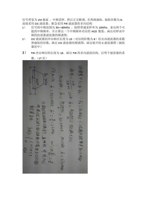
信号带宽为1M赫兹,中频采样,然后正交解调,在两级抽取,抽取倍数为9,前级采用CIC滤波器,猴急采用FIR滤波器的多向结构
1)信号的中频范围为50—60Mhz ,按照带通采样率为10Mhz,求出两个可能的中频频率,并计算出一个中频频率对应的NCO数值,画出对样该中频的抗混叠滤波器的频谱图,
2)CIC滤波器的冲击响应长度为10(对应的阶数为9)给出该滤波器的系数和抽取的倍数,画出CIC滤波器的频谱图,画出展开的C滤波器图(抽取器居中)
3)FIR冲击响应的长度为18,画出FIR的多向滤波结构,注明个滤波器的系数。
(17页)
对单通道朝外差数字中频接收机,其接受信号的射频频率为fRF=108Mhz,信号中频频率为fIF=36Mhz,信号带宽为8Mhz
根据带通采样定理设计中频采样频率fs和扩展带宽bs* (信道处理带宽)
画出中频采样钱康混叠滤波器幅频示意图。
长风破浪会有时,直挂云帆济沧海。
住在富人区的她电子科技大学智慧树知到“电子信息工程”《高频电路》网课测试题答案(图片大小可自由调整)第1卷一.综合考核(共10题)1.若非线性器件的伏安特性幂级数表示,式中是不为零的常熟,信号u是频率为150kHz和200kHz的两个正弦波,以下哪个频率成分是不能够出现的?()A.300kHzB.50kHzC.400kHzD.100kHz2.以下哪个不属于无线通信调制的基本方式?()A.振幅调制(M)B.混合调制(MM)C.频率调制(FM)D.相位调制(PM)3.串联型石英晶振中,石英谐振器相当于()元件A.电容B.电阻C.电感D.短路线4.某调频波,其调制信号频率F=1kHz,载波频率为10.7MHz,最大频偏Δfm=10kHz,若调制信号的振幅不变,频率加倍,则此时调频波的频带宽度为()A.12kHzB.24kHzC.20kHzD.40kHz5.按照无线电波的频段划分,以下哪种不属于微波波段?()A.超短波(VSW)B.分米波(USW)C.厘米波(SSW)D.毫米波(ESW)6.高频小信号放大器的输入导纳为()。
A.B.C.D.7.高频谐振放大器中,哪些不是造成工作不稳定的主要因素?()A.集电结电容B.基极电感C.环境温度的改变会使晶体管参数发生变化D.负载阻抗过大,增益过高引起的自激振荡8.高频谐振功率放大器用于基极调幅,谐振功放的工作状态是()。
A.过压状态B.欠压状态C.临界状态D.略欠压状态9.频率为100Hz的载波被频率被5kHz的正弦信号调制,最大频偏为50kHz。
则此时FM波的带宽为()。
A.50KHzB.110KHzC.150KHzD.210KHz10.以下哪些功能模块不需要高频振荡器?()A.信号源B.载波信号C.本地振荡信号D.放大器长风破浪会有时,直挂云帆济沧海。
住在富人区的她第1卷参考答案一.综合考核1.参考答案:D2.参考答案:B3.参考答案:D4.参考答案:B5.参考答案:A6.参考答案:B7.参考答案:B8.参考答案:B9.参考答案:B10.参考答案:D。
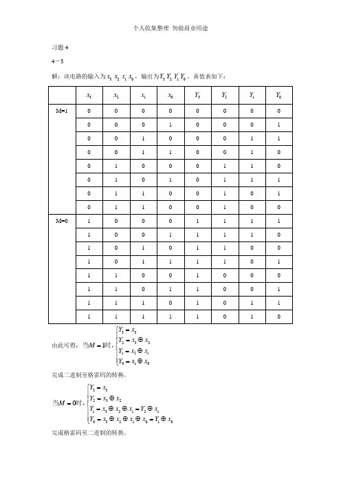
习题4 4-3解:该电路的输入为3x 2x 1x 0x ,输出为3Y 2Y 1Y 0Y 。
真值表如下:由此可得:1M =当时,33232121010Y x Y x x Y x x Y x x =⎧⎪=⊕⎪⎨=⊕⎪⎪=⊕⎩ 完成二进制至格雷码的转换。
0M =当时,332321321210321010Y x Y x x Y x x x Y x Y x x x x Y x =⎧⎪=⊕⎪⎨=⊕⊕=⊕⎪⎪=⊕⊕⊕=⊕⎩ 完成格雷码至二进制的转换。
4-9 设计一个全加(减)器,其输入为A,B,C 和X (当X =0时,实现加法运算;当X =1时,实现减法运算),输出为S(表示和或差),P(表示进位或借位)。
列出真值表,试用3个异或门和3个与非门实现该电路,画出逻辑电路图。
解:根据全加器和全减器的原理,我们可以作出如下的真值表:由真值表可以画出卡诺图,由卡诺图得出逻辑表达式,并画出逻辑电路图:A B C XP4-10 设计一个交通灯故障检测电路,要求红,黄,绿三个灯仅有一个灯亮时,输出F =0;若无灯亮或有两个以上的灯亮,则均为故障,输出F =1。
试用最少的非门和与非门实现该电路。
要求列出真值表,化简逻辑函数,并指出所有74系列器件的型号. 解:根据题意,我们可以列出真值表如下:对上述的真值表可以作出卡诺图,由卡诺图我们可以得出以下的逻辑函数:F AB AC BC ABC AB AC BC ABC =+++=•••逻辑电路图如下所示:A F4-13 试用一片3-8译码器和少量逻辑门设计下列多地址输入的译码电路.(1) 有8根地址输入线7A ~1A ,要求当地址码为A8H,A9H ,…,AFH 时,译码器输出为0Y ~7Y 分别被译中,且地电平有效。
(2) 有10根地址输入线9A ~0A ,要求当地址码为2E0H,2E1H, …,2E7H 时,译码器输出0Y ~7Y 分别被译中,且地电平有效.解:(1)当122100A B E E E =,即75364210111,00,A A A A A A A A ==从000~111变化时07~Y Y 分别被译中,电路如下图所示:Y Y (2)当122100A B E E E =,即97538432101111,000,A A A A A A A A A A ==从000~111变化时,07~Y Y 分别被译中。
电子科大数字通信理论考试答案电子科大数字通信理论考试答案————————————————————————————————作者:————————————————————————————————日期:电子科技大学研究生试卷(考试时间: 10:00 至 12:00 ,共 2小时)课程名称数字通信理论教师李兴明、许勃学时 40 学分 2 教学方式课堂授课考核日期 2012 年 5 月 10 日成绩考核方式:(学生填写)一、填空题:(30分)1 某二维信号用向量表示为 S i =[3,4], 该信号的能量为 25 。
2 如下数字调制方法:M 元QAM , M 元正交信号,M 元PSK ,M 元PAM ,M 元双正交信号,MSK ,其中, M 元QAM , M 元PSK , M 元PAM ,MSK 适合于带宽受限信道,M 元正交信号, M 元双正交信号适合于功率受限信道。
3一个数字传输系统以1000符号/秒的码元速率传送16进制码元,该系统的信息速率是_________4000_______________bps 。
4 假设信号的符号间隔为50ms ,为了保证信号的正交性,FSK 相干检测时要求的最小频率间隔为__10Hz ,非相干检测时要求的最小频率间隔为______20Hz___ ___。
5 2PAM, 2FSK, 2PSK 和2DPSK 四种数字调制信号通过AWGN 信道传输。
假设发送信号的幅度相同,信息速率相同,噪声的功率谱密度N 0相同,接收端都采用理想的相干最佳解调,那么,在大信噪比条件下,将这4种调制方式按误比特率从小到大排出的次序是________2PSK, 2DPSK, 2FSK, 2PAM ____ ____。
6 四元PAM 信号调制在频率为25MHz 的载波上,通过AWGN 信道传送,信道传输延迟为0.01μs ,则由此产生的相位偏移是_________-0.5π, -π/2 ____________。

无线电期末考试试卷与答案一、判断题(每题1分,共15分)1.数字电路中三极管一般工作在放大状态.(X )2.或门电路的逻辑功能可概括为有“有0出0,全1出0”.(X )3.集成MOS逻辑门电路保存时一般应将各脚短接.( √ )4.计算机开机时应先开主机后开外部设备,关机时应先关主机后关外部设备.(X )5.“桌面”是指WINDONWS启动后,出现在屏蔽上的整个区域.(√ )6. 调频广播不易受到干扰,接收效果好,发射距离远.( X)7.检验员个人有权利对产品实行免检.( X )8.建立质量体系的目的是为了迎接质量体系认证和上级审核.( X )9.不管有什么理由,自己都不能保留已作废的文件和元器件.( √ )10.检验和实验状态的标识不是唯一的,而产品标识都是唯一的.( √ )11.各单位根据人员调配和岗位变更,核查其岗位证书,将无证和转岗人员报送质保部.( X )12.检验员应严格按照产品图样、技术条件和工艺文件检验产品,正确判断产品合格与否,对不合格品进行标识和隔离并填写不合格品报告.( √ )13.检验人员负责不合格的处理.( X )14.对三件以上的工件,应进行首件三检.( √ )15.对由主观原因造成质量损失的单位或单价应进行惩罚.( √)二、选择题(每题2分,共30分)1、在印制板焊接中,光铜线跨接另一端头时,如有线路(底部),或容易碰撞其他器件时,应加套( A)。
A、聚四氟乙烯套管B、热缩套管C、聚氯乙烯套管D、电气套管2、在组装整机装配时,应使用哪几份装配图纸,来完成装配过程:( C )。
A、机械铆装图和接线图B、机械装配图和线缆连接线图C、机械装配图和接线图D、机械装配图和接线图及线缆连接线图3、在整机调试过程,应使用哪几份图纸文件,来完成调试要求:( D )。
A、调试说明和电路图及软件程序B、技术说明和电路图及线缆连接线图C、调试说明和技术说明及电路图D、调试说明和电路图及线缆连接线图4、螺母、平垫圈和弹簧垫圈要根据不同的情况合理使用,不允许任意增加或减少。
信号与系统习题解答11.1 用代数式表达下列复数:已知形式为θj re ,要求表达形式为jy x +,采用公式:θcos r x =,θsin r y =。
解: 2121-=πj e 2121-=-πj ej e j =2π j e j -=-2πj ej=25πj ej+=124π j ej+=1249πj ej -=-1249π j ej-=-124π1.2 用极式表达下列复数:已知形式为jy x +,要求表达形式为θj re ,采用公式:22y x r +=,()πθπθ≤<-=-xytg 1。
解:055j e = πj e 22=- 233πjej -=-()2242221ππjj e e j --=⎪⎪⎭⎫ ⎝⎛=- ()442221πππjjje eej j =⋅=--2442211πππjjje ee jj ==-+-1234223122πππjj je e ej j -==++1.54 (a )证明表达式 ⎪⎩⎪⎨⎧≠--==∑-=111110αααααN N n nN证: 因为 1=α 时,1=n α (n 为任意值时)所以,1=α 时,N N n n =∑-=10α因为 ()()NN ααααα-=++++--1 (111)2所以,当1≠α时,()ααααα--=++++-11 (11)2NN 原式得证。
(b) 证明:1<α时,αα-=∑∞=110n n 证:因为 1<α时,0lim ==∞→NN α所以:αααα-=--=∞→∞=∑1111lim 0N N n n(c )证明:1<α时,()21ααα-=∑∞=n nn 证:令()αααf n n=-=∑∞=11为α的连续函数对上式进行微分运算可得:()()2111αααα-==∑∞=-n n n d df 同时乘以α就可以得到:()21αααααα-==∑∞=n nn d df (d )当1<α时,计算?=∑∞=kn nα解: 因为∑∑∑∞=-=∞=+=kn nk n n n n ααα100所以:αααααααα-=----=-=∑∑∑-=∞=∞=1111110kk k n nn nk n n1.55 计算下列和式,采用代数式表达。
1.计算序列x(n)的256点DFT,需要的复数乘法次数为 ( ) 。
A.256B.256×256C.256×255D.128×8【参考答案】: B2.下列关于FIR滤波器的说法中正确的是()A.FIR滤波器容易设计成线性相位特性B.FIR滤波器的脉冲响应长度是无限的C.FIR滤波器的脉冲响应长度是确定的D.对于相同的幅频特性要求,用FIR滤波器实现要比用IIR滤波器实现阶数低【参考答案】: C3.实序列傅里叶变换的实部和虚部分别为( )。
A.偶函数和奇函数B.奇函数和偶函数C.奇函数和奇函数D.偶函数和偶函数【参考答案】: A4.序列x(n)=u(n)的能量为()。
A.1B.9C.11D.∞【参考答案】: D5.要处理一个连续时间信号,对其进行采样的频率为3kHz,要不失真的恢复该连续信号,则该连续信号的最高频率可能是为( )。
A.6kHzB.1、5kHzC.3kHzD.2kHz【参考答案】: B6.以下对有限长单位冲激响应(FIR)滤波器特点的论述中错误的是( )。
A.FIR滤波器容易设计成线性相位特性B.FIR滤波器的单位冲激抽样响应h(n)在有限个n值处不为零 C.系统函数H(z)的极点都在z=0处 D.实现结构只能是非递归结构【参考答案】: D7.下面关于IIR滤波器设计说法正确的是( )。
A.双线性变换法的优点是数字频率和模拟频率成线性关系B.冲激响应不变法无频率混叠现象 C.冲激响应不变法不适合设计高通滤波器 D.双线性变换法只适合设计低通、带通滤波器【参考答案】: C8.下列关于用冲激响应不变法设计IIR滤波器的说法中错误的是( )、A.数字频率与模拟频率之间呈线性关系B.能将稳定的模拟滤波器映射为一个稳定的数字滤波器 C.使用的变换是s平面到z平面的多值映射 D.可以用于设计低通、高通和带阻等各类滤波器【参考答案】: D9.在窗函数法的FIR滤波器设计法中,滤波器过渡带宽度近似等于窗函数幅度谱的主瓣宽度的()倍。
作业 1:FM 对讲机中接收机的设计 系统参数:射频频率: 433MHz信号带宽:15KHz (频偏 7.5KHz ,音频带宽 3.4KHz ) 调制方式:FM 要求:1. 给出一个可实现的系统结构 2. 设计系统各级的主要参数(如滤波器、振荡器等) 3. 画出各级的频谱结构答案: 1. 二次变频超外差式接收机系统:f0 433MHz B 20MHzf IF149.5MHzf0 49.5MHz B 100KHzfIF2 450KHzf0 450KHz B 15KHzfLO1 383.5MHz 或 482.5MHzfLO2 48.05MHz 或 49.95MHz2.15KHz433f (MHz)334 383.5 433 482.5 532 f (MHz)47.5 48.05 49.5 49.95 50.4 f (MHz)450f (KHz)1.根据下图所示的数字基带接收机电路和 A 点给定的信号频谱, 画出图中 B、C、D、E、F 点的信号频谱。
cos0te j0t e 2j0tAsin 0tej0t e 2jj0tcosotLPFLPF-sinotzBI(t)zBI(n)BC zBQ(t)A/DDDSPEA/DzBQ(n)fs=2.5BszB(n)= zBI(n) +j zBQ(n)FA点信号频谱:X(f)1Bs0.5 f0 Bs f00f0 f0 Bs f (Hz)答案:B点信号频谱: 经LPF滤除2 f0ZBI ( f ) 1 0.5Bs 0 Bs经LPF滤除2 f0 f (Hz)C点信号频谱:j ZBQ ( f ) 10.5Bs0 Bsf (Hz)D点信号频谱:ZBI () 10.52.5Bs Bs 0 Bs 1.5Bs 2.5Bs 2 0.8 0 0.8 1.2 2 1 0.4 0 0.4 0.6 1E点信号频谱:j ZBQ () 10.50.81.22 1.2 0 0.82f (Hz) (rad)f fs (rad)F点信号频谱:2.5Bs 2 1ZB () ZBI () jZBQ () 1 0.50 Bs 0 0.8 0 0.42.5Bs 2 1f (Hz) (rad)f fs作业 3:调频广播带通采样数字中频接收机设计。
学院_______________________ 系别____________ 班次_____________ 学号__________ 姓名________________………….……密…..……….封……..……线………..…以………..…内………....答…………...题…………..无…….….效…..………………..电子科技大学《通信原理》课程试题(B 卷)(120分钟)一 二三四五六七八九十总分评卷教师1. Blank Filling:(1) A analog waveform can be converted to digital signal (for a PCM system) by three basic operations:sampling 、 quantizing 、 coding .(2) A law and µ law companding is the two main nonuniform quantizing used in PCM system.(3) The input amplitude of a linear circuit is 5V .The output amplitude is 10V . Then the gain of the circuit is 6dB.(4) BANDPASS SAMPLING THEOREM: If a (real) bandpass waveform has a nonzero spectrum only over thefrequency interval f 1 < | f | < f 2, where the transmission bandwidth B T is taken to be the absolute bandwidth B T = f 2 – f 1, then the waveform may be reproduced from sample values if the sampling rate is fs=2B T .(5) All communications systems involve three main subsystems : transmitter 、 channel 、 receiver .2. Multiple Choice:(1) If the bandwidth of an modulation signal m(t) is f 0, the bandwidth of AM, DSB-SC and SSB signal are_____(A)________ respectively(A) 2f 0, 2f 0, f 0 (B) f 0, 2f 0, f 0 (C) 2f 0, f 0, 2f 0 (D) 2f 0, 2f 0, 2f 0(2) In the following definition, the right is __(D)______(A) A bandpass waveform has a spectral magnitude that is zero for the frequency in the vicinity of the origin andnegligible elsewhere(B) A baseband waveform has a spectral magnitude that is zero for the frequency in some band concentratedabout a frequencyc f f ±=, where 0f c >>, and negligible elsewhere(C) Modulation is the process of imparting the source information onto a bandpass signal with a carrierfrequency by introduction of amplitude or phase perturbations or both. The baseband source signal is called the modulated signal(D) Modulation is the process of imparting the source information onto a bandpass signal with a carrierfrequency by introduction of amplitude or phase perturbations or both. The baseband source signal is called the modulating signal.(3) In a communication system, the random data pattern consist of binary 1’s and 0’s, and its PSD is22sin(/2)()||4/2b b s b A T fT f fT ππ=Pwhere RT b 1= is the time needed to send 1 bit of data. The first-null bandwidth of the signal and thebandwidth efficiency are__(C)____respectly(A) R, 1 (B)4R, 0.25 (C) 2R, 0.5 (D) R, 1(4) If the PSD(Power Spectral Density) of a baseband signal s(t) is shown in the following figure, the absolutebandwidth 、3dB bandwidth and first zero-crossing bandwidth is___(D)_______ respectively.(A) f3 f2, (f1+f3)/2(B) f3, f2, (f1+f2)/2(C) f2, f3, (f1+f2)/2 (D) f3, (f1+f2)/2, f2(5)The amplitude spectra of a Raised cosine-rolloff signal is shown in the following Figure, its 6-dB bandwidth is-__(B) ____(A) (B T+f1)/4(B) (B T+f1)/2(C) (B T-f1)(D) f1(6)For distortionless transmission of bandpass signal, the channel transfer function need to satisfy__(D)______(A) The amplitude response or phase response is constant(B) The product of the amplitude response and phase response are constant(C) The amplitude response or the derivative of the phase response is constant(D)Both the amplitude response and the derivative of the phase response are constant(7)In the following description about MSK, the wrong is __(B)___(E)_____(A) MSK is a continuous FSK(B) MSK’s modulation index is minimum, and equal to 1(C) Two signals representing ‘1’ and ‘0’ are ortho gonal over the bit interval(D) MSK is identical with OQPSK when the pulse shape is sinusoidal type(E) MSK bandwidth is 3R/2 when the transmission rate of baseband signal is R(8)In the following description about QPSK, π/4 QPSK and OQPSK signal, the wrong is ___(D)______(A) They are 4-ary modulated bandpass signaling(B) For rectangular-shaped data pulses, the envelope of the QPSK signal is constant and there is no AM on thesignal(C) For nonrectangular-shaped data pulses, the phase shift and AM of QPSK are the maximum ,while the phaseshift and AM of OQPSK are the minimum(D) For rectangular-shape data pulses, the phase shift and AM of QPSK are the maximum while the phase shiftand AM of OQPSK are the minimum(9)In the following description about the matched filter, the right is ____(B)___(A) MF is a Gaussian filter(B) MF maximize the instantaneous output signal power to the average output noise power for a given inputsignal waveshape(C)For the case of white noise, the impulse response of MF is h(t)=Cs(-t) when the input signal is s(t) and C is aconstant(D)Realizing forms have the integrate-and-dump method, the correlator method and the LPF configurations(10)N onlinear amplifier output-to-input characteristic, hard (ideal) limiter characteristic and envelope detector’soutput-to-input characteristic are__(A)_____ respectivelyFig.1 Fig.2 Fig.3(A) Fig.2, Fig.3 and Fig.1 (B) Fig.1, Fig.2 and Fig.3(C) Fig.3, Fig.2 and Fig.1 (D) Fig.2, Fig.2 and Fig.13. A binary base band signal (polar NRZ) is passed through a transmitted system, the data rate is 26Mb/s, and the transponder has a bandwidth of 100MHz.(a)If the system is a base band communication system, what is the null-to-null bandwidth of transmitted signal,what is the minimum transmission bandwidth for it?(b)If the base band signal is modulated by a carrier (using BPSK, and the carrier frequency is 10GHz) and thenbe transmitted through band pass communication system, what is the null-to-null bandwidth of transmitted signal, what is the minimum transmission bandwidth for it?(c)In question b), if the base band signal is passed through a raised cosine roll off filter with a 50% roll offfactor and is then modulated onto the carrier, what is the transmission bandwidth for it?(d)If QPSK and the raised cosine roll off filter with a 50% roll off factor are used, what is the maximum data rate that the band pass system can support?Solution: (a)min26132null RB R MHz B MHz ==== (b)min2522262null RB R MHz B MHz ===⋅=(c)(1)26 1.539T B R r MHz =+=⨯=(d)max (1)(1)2200100 1.5133.3/2 1.5T RB D r r R R Mb s=+=+=⨯==4. A modulated RF waveform is given by[]t cos 50t cos 200i c ω+ω, where ,kHz 2f i = and.MHz 90f c =(a)If the phase deviation constant is 200 rad/V , find the mathematical expression for the corresponding PMvoltage m(t). What is the peak phase deviation? (b) If the frequency deviation constant is 106 rad/V-s, find the mathematical expression for the correspondingFM voltage m(t). What is the peak frequency deviation? (c) If the RF waveform appears across a 50Ω load, determine the average power and the PEP. Solution: (a)()()[]()()cos 200cos 50cos 50cos 50cos 400050200PM c c P c i P i S A t D m t t t D m t t m t tωωωωπθ=+=+∴=∴=∆=(b)()()[]()()()()65cos 200cos 50cos 50cos 50cos 4000504000sin 40000.2sin 40001011504000sin 40002210tFM c c f c i tf i d S A t D m d t t D m d t tm t t td t f t t dt F Hzωσσωωσσωπππππθππππ-∞-∞=+=+∴==∴=-⋅⋅=-⎡⎤==-⨯⨯⋅⎢⎥⎣⎦∴∆=⎰⎰5. The equivalent transfer function of a binary baseband system is as:()⎪⎩⎪⎨⎧τ≤τπ+τ=other ,021f ,f 2cos 1)f (H 000(a) Find the maxmum baud rate that is no ISI. (b) Find the spectral efficiency of this system.Solution: (a)000111(1)22(11)2D r D τττ+=→==+(b) 1/TD Bd Hz B η==6. Eleven analog signal, each with a bandwidth of 3400Hz, are sampled at an 8kHz rate and multiplexed together witha synchronization channel(8kHz) into a TDM PAM signal, Assume that the analog samples will be encoded into 4-bit PCM words. Then the TDM PCM signal is pass though a channel with an overall raised cosine-rolloff Nyquistfilter characteristic of 75.0=γ . (a) Indicating the multiplexing rate f s , and the overall bit rate of the TDM PCM signal. (b)Evaluate the absolute bandwidth required for the channel.Solution: (a) 8s f kHz =121248384/s R nf kb s ==⨯⨯=(b)()384(1) 1.75336()22T R B kHz γ=+==7. The receiver is shown in Fig 7. Assume that the Bandpass input signaling is)t (n )t f 2cos(200)t f 2cos()t 800sin(100)t (r c c +π+ππ= [V],where n(t) is white noise with a PSD of20102/N -= [W/Hz]. Find the out )N /S (Figure 7Solution:()100sin(800)cos(2)200cos(2)1200cos(2)1sin(800)2AM c c c s t t f t f t f t t πππππ=+⎡⎤=+⎢⎥⎣⎦()()()2222230111200sin(800)2281200831.252221041010lg 14.9C m c outoutA m t t A m t A m t S N NB S dBN π-====⨯⎛⎫=== ⎪⨯⨯⨯⨯⎝⎭⎛⎫= ⎪⎝⎭8.Assume that the input signal ⎩⎨⎧≤<=-otherwise ,0T t 0 ,e )t (s t is a known signal. Finda) The impulse response of the matched filter for the case of white noise.b) The maximum signal level occurs at the matched filter output.Solution:()(), 0t T ()0, otherwise T t e h t s T t --⎧<≤⎪=-=⎨⎪⎩()()2220112T TtTo s T s t dt e dt e --⎡⎤===-⎣⎦⎰⎰。
第一章测试1.1887年,德国科学家赫兹证明了电磁波的存在。
()A:错B:对答案:B2.当电流在天线中流动时,天线周围的空间不但产生电力线,同时产生磁力线。
()A:错B:对答案:B3.八木天线天线一般用于80米测向机的天线。
()A:错B:对答案:A4.常见的天线种类有四种,分别是:直立天线,环形天线,磁性天线还有八木天线。
()A:错B:对答案:B5.短距离80米波段信号源发射的电磁波是水平极化波。
()A:错B:对答案:A第二章测试1.信号源的首要任务就是接受信号且把它传播出去。
()A:错B:对答案:A2.无线电测向机的任务就是接受信号。
()A:错B:对答案:B3.信号源在未安装发射天线,禁止开机,否则会造成发射电路损坏,信号源出现严重故障。
()A:错B:对答案:B4.2米测向机天线振子与地面要保持在同一平面,从而保证测向天线处于最佳接受状态。
()A:对B:错答案:A5.运动员在预备区刷清除站,然后领取测向机,此时测向机就可以开始使用。
()A:错B:对答案:A第三章测试1.80米波段测向中,当收测完6号电台信号后,接下来要收测5号台时,应将调谐旋钮沿顺时针方向旋转。
()A:错B:对答案:A2.沿测向机指示的电台方向,边跑边测,直接接近电台的方法叫方向跟踪方向跟踪。
()A:对B:错答案:A3.MO号电台是终点台。
()A:错B:对答案:B4.0号台台码为:—–。
()A:对B:错答案:A5.比音量有两种方法,一种是扫音量,另一种是跑音量。
()A:错B:对答案:B第四章测试1.运动员接到出发指令,起点出发后,直接离开起点,寻找首找台。
()A:对B:错答案:B2.在2米波段,高处的电磁波强度略高一些,因此都会将测向机高举,收到信号后,再进行判断电台的方位。
()A:错B:对答案:B3.小角度布台的策略方法,当终点台方向线偏向一边或者最外侧时,可暂时选择与终点台夹角最大的台,作为首找台。
()A:对B:错答案:A4.方向跟踪法多应用于地形简单、障碍较少,比赛中能在电台发信时间内到达电台的情况下使用,在比赛中,根据实际地形,我们一般采用直接跟踪和弧形跟踪相结合的方法来锁定电台。
专业无线电考试题及答案一、单项选择题1. 无线电波的传播方式不包括以下哪一项?A. 地波传播B. 天波传播C. 直线传播D. 反射传播答案:C2. 无线电发射机的主要功能是什么?A. 放大信号B. 调制信号C. 转换信号D. 以上都是答案:D3. 在无线电通信中,调制的目的是什么?A. 提高信号的传输距离B. 增加信号的功率C. 将信息信号加载到载波上D. 改变信号的频率答案:C4. 无线电频率的单位是什么?A. 赫兹(Hz)B. 瓦特(W)C. 安培(A)D. 欧姆(Ω)答案:A5. 无线电波的波长和频率之间的关系是什么?A. 波长与频率成正比B. 波长与频率成反比C. 波长与频率无关D. 波长与频率相等答案:B二、多项选择题1. 无线电波的传播方式包括哪些?A. 地波传播B. 天波传播C. 直线传播D. 散射传播答案:A、B、C、D2. 无线电通信中常用的调制方式有哪些?A. 调幅(AM)B. 调频(FM)C. 调相(PM)D. 数字调制答案:A、B、C、D3. 无线电波的传播特性包括哪些?A. 直线传播B. 反射C. 折射D. 衍射答案:A、B、C、D三、判断题1. 无线电波在真空中的传播速度等于光速。
A. 正确B. 错误答案:A2. 无线电波的频率越高,波长越长。
A. 正确B. 错误答案:B3. 无线电波的功率越大,传输距离越远。
A. 正确B. 错误答案:A4. 无线电波的调制过程不会改变载波的频率。
A. 正确B. 错误答案:B四、填空题1. 无线电波的传播速度是______米/秒。
答案:2997924582. 无线电波的波长和频率之间的关系可以用公式______表示。
答案:c = λf3. 无线电波的调制方式中,调频(FM)的特点是频率随______变化而变化。
答案:振幅4. 无线电波的传播方式中,______传播是无线电波沿地球表面传播的方式。
答案:地波五、简答题1. 简述无线电波的直线传播原理。