TDA7293英文手册
- 格式:pdf
- 大小:342.41 KB
- 文档页数:13
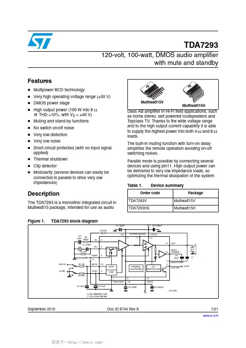
TDA7293120V -100W DMOS AUDIO AMPLIFIER WITH MUTE/ST-BYVERY HIGH OPERATING VOLTAGE RANGE (±50V)DMOS POWER STAGEHIGH OUTPUT POWER (100W @THD =10%,R L =8Ω,V S =±40V)MUTING/STAND-BY FUNCTIONS NO SWITCH ON/OFF NOISE VERY LOW DISTORTION VERY LOW NOISESHORT CIRCUIT PROTECTION THERMAL SHUTDOWN CLIP DETECTORMODULARITY (MORE DEVICES CAN BE EASILY CONNECTED IN PARALLEL TO DRIVE VERY LOW IMPEDANCES)DESCRIPTIONThe TDA7293is a monolithic integrated circuit in Multiwatt15package,intended for use as audio class AB amplifier in Hi-Fi field applications (Home Stereo,self powered loudspeakers,Top-class TV).Thanks to the wide voltage range and to the high out current capability it is able to sup-ply the highest power into both 4Ωand 8Ωloads.The built in muting function with turn on delay simplifies the remote operation avoiding switching on-off noises.Parallel mode is made possible by connecting more device through of pin11.High output power can be delivered to very low impedance loads,so optimizing the thermal dissipation of the system.December1999®IN-2R2680ΩC222µF C1470nF IN+R122K3R322K-+MUTESTBY4VMUTE VSTBY109SGND MUTE STBYR422KTHERMAL SHUTDOWNS/CPROTECTIONR510KC310µFC410µF1STBY-GNDC5 22µF713146158-Vs -PWVsBOOTSTRAP OUT +PWVs +VsC9100nFC81000µF-VsD97AU805A+VsC7100nFC61000µFBUFFER DRIVER11BOOT LOADER125VCLIPCLIP DET(*)(*)see Application note (**)for SLAVE function(**)Figure 1:Typical Application and Test CircuitMultiwatt15ORDERING NUMBER:TDA7293VMULTIPOWER BCD TECHNOLOGY1/13ABSOLUTE MAXIMUM RATINGSSymbol ParameterValue Unit V S Supply Voltage (No Signal)±60V V 1V STAND-BY GND Voltage Referred to -V S (pin 8)90V V 2Input Voltage (inverting)Referred to -V S 90V V 2-V 3Maximum Differential Inputs±30V V 3Input Voltage (non inverting)Referred to -V S 90V V 4Signal GND Voltage Referred to -V S 90V V 5Clip Detector Voltage Referred to -V S 120V V 6Bootstrap Voltage Referred to -V S 120V V 9Stand-by Voltage Referred to -V S 120V V 10Mute Voltage Referred to -V S 120V V 11Buffer Voltage Referred to -V S120V V 12Bootstrap Loader Voltage Referred to -V S 100V I O Output Peak Current10A P tot Power Dissipation T case =70°C 50W T op Operating Ambient Temperature Range 0to 70°C T stg ,T jStorage and Junction Temperature150°C1234567910118BUFFER DRIVER MUTE STAND-BY -V S (SIGNAL)+V S (SIGNAL)BOOTSTRAPCLIP AND SHORT CIRCUIT DETECTOR SIGNAL GROUND NON INVERTING INPUT INVERTING INPUT STAND-BY GNDTAB CONNECTED TO PIN 813141512-V S (POWER)OUT+V S (POWER)BOOTSTRAP LOADER D97AU806PIN CONNECTION (Top view)QUICK REFERENCE DATASymbol ParameterTest ConditionsMin.Typ.Max.Unit V S Supply Voltage Operating ±12æ50V G LOOP Closed Loop Gain 2640dB P tot Output PowerV S =±45V;R L =8Ω;THD =10%140W V S =±30V;R L =4Ω;THD =10%110W SVRSupply Voltage Rejection75dBTHERMAL DATASymbol DescriptionTyp Max Unit R th j-case Thermal Resistance Junction-case11.5°C/WTDA72932/13ELECTRICAL CHARACTERISTICS(Refer to the Test Circuit V S=±40V,R L=8Ω,R g=50Ω;T amb=25°C,f=1kHz;unless otherwise specified).Symbol Parameter Test Condition Min.Typ.Max.Unit V S Supply Range±12±50VI q Quiescent Current30mAI b Input Bias Current0.31µAV OS Input Offset Voltage-1010mVI OS Input Offset Current0.2µAP O RMS Continuous Output Power d=1%:R L=4Ω; V S=±29V,8080Wd=10%R L=4Ω ;V S=±29V 100100Wd Total Harmonic Distortion(**)P O=5W;f=1kHzP O=0.1to50W;f=20Hz to15kHz 0.0050.1%%I SC Current Limiter Threshold 6.5A SR Slew Rate15V/µs G V Open Loop Voltage Gain80dB G V Closed Loop Voltage Gain(1)30dBe N Total Input Noise A=curvef=20Hz to20kHz 125µVµVR i Input Resistance100kΩSVR Supply Voltage Rejection f=100Hz;V ripple=0.5Vrms75dB T S Thermal Protection DEVICE MUTED150°CDEVICE SHUT DOWN160°C STAND-BY FUNCTION(Ref:to pin1)V ST on Stand-by on Threshold 1.5V V ST off Stand-by off Threshold 3.5V ATT st-by Stand-by Attenuation7090dBI q st-by Quiescent Current@Stand-by0.5mA MUTE FUNCTION(Ref:to pin1)V Mon Mute on Threshold 1.5V V Moff Mute off Threshold 3.5V ATT mute Mute AttenuatIon6080dB CLIP DETECTORDuty Duty Cycle(pin5)THD=1%;RL=10KΩ to5V10%THD=10%;RL=10KΩto5V40%I CLEAK PO=50W1µA SLAVE FUNCTION pin4(Ref:to pin8-V S)V Slave SlaveThreshold1V V Master Master Threshold3V Note(1):G Vmin≥26dBNote:Pin11only for modular connection.Max external load1MΩ/10pF,only for test purposeNote(**):Tested with optimized Application Board(see fig.2)TDA72933/13TDA7293Figure2:Typical Application P.C.Board and Component Layout(scale1:1) 4/13APPLICATION SUGGESTIONS (see Test and Application Circuits of the Fig.1)The recommended values of the external components are those shown on the application circuit of Fig-ure 1.Different values can be used;the following table can help the designer.COMPONENTSSUGGESTED VALUEPURPOSE LARGER THAN SUGGESTED SMALLER THAN SUGGESTED R1(*)22k INPUT RESISTANCEINCREASE INPUT IMPEDANCEDECREASE INPUT IMPEDANCER2680ΩCLOSED LOOP GAIN SET TO 30dB (**)DECREASE OF GAIN INCREASE OF GAIN R3(*)22k INCREASE OF GAIN DECREASE OF GAINR422kST-BY TIME CONSTANT LARGER ST-BY ON/OFF TIME SMALLER ST-BY ON/OFF TIME;POP NOISE R510k MUTE TIME CONSTANT LARGER MUTE ON/OFF TIMESMALLER MUTE ON/OFF TIME C10.47µFINPUT DC DECOUPLING HIGHER LOW FREQUENCY CUTOFF C222µFFEEDBACK DC DECOUPLING HIGHER LOW FREQUENCY CUTOFF C310µF MUTE TIME CONSTANT LARGER MUTE ON/OFF TIME SMALLER MUTE ON/OFF TIME C410µFST-BY TIME CONSTANT LARGER ST-BY ON/OFF TIME SMALLER ST-BY ON/OFF TIME;POP NOISE C522µFXN (***)BOOTSTRAPPINGSIGNALDEGRADATION AT LOW FREQUENCYC6,C81000µF SUPPLY VOLTAGEBYPASS C7,C90.1µFSUPPLY VOLTAGEBYPASSDANGER OF OSCILLATION(*)R1=R3for pop optimization(**)Closed Loop Gain has to be ≥26dB(***)Multiplay this value for the number of modular part connectedMASTERUNDEFINEDSLAVE-V S +3V-V S +1V-V SD98AU821Slave function:pin 4(Ref to pin 8-V S )Note:If in the application,the speakers are connected via long wires,it is a good rule to add between the output and GND,a BoucherotCell,in order to avoid dangerous spurious oscillations when the speakers terminal are shorted.The suggested Boucherot Resistor is 3.9Ω/2W and the capacitor is 1µF.TDA72935/13INTRODUCTIONIn consumer electronics,an increasing demand has arisen for very high power monolithic audio amplifiers able to match,with a low cost,the per-formance obtained from the best discrete de-signs.The task of realizing this linear integrated circuit in conventional bipolar technology is made ex-tremely difficult by the occurence of2nd break-down phoenomenon.It limits the safe operating area(SOA)of the power devices,and,as a con-sequence,the maximum attainable output power, especially in presence of highly reactive loads. Moreover,full exploitation of the SOA translates into a substantial increase in circuit and layout complexity due to the need of sophisticated pro-tection circuits.To overcome these substantial drawbacks,the use of power MOS devices,which are immune from secondary breakdown is highly desirable. The device described has therefore been devel-oped in a mixed bipolar-MOS high voltage tech-nology called BCDII100/120.1)Output StageThe main design task in developping a power op-erational amplifier,independently of the technol-ogy used,is that of realization of the output stage. The solution shown as a principle shematic by Fig3represents the DMOS unity-gain output buffer of the TDA7293.This large-signal,high-power buffer must be ca-pable of handling extremely high current and volt-age levels while maintaining acceptably low har-monic distortion and good behaviour over frequency response;moreover,an accurate con-trol of quiescent current is required.A local linearizing feedback,provided by differen-tial amplifier A,is used to fullfil the above require-ments,allowing a simple and effective quiescent current setting.Proper biasing of the power output transistors alone is however not enough to guarantee the ab-sence of crossover distortion.While a linearization of the DC transfer charac-teristic of the stage is obtained,the dynamic be-haviour of the system must be taken into account.A significant aid in keeping the distortion contrib-uted by the final stage as low as possible is pro-vided by the compensation scheme,which ex-ploits the direct connection of the Miller capacitor at the amplifier’s output to introduce a local AC feedback path enclosing the output stage itself.2)ProtectionsIn designing a power IC,particular attention must be reserved to the circuits devoted to protection of the device from short circuit or overload condi-tions.Due to the absence of the2nd breakdown phe-nomenon,the SOA of the power DMOS transis-tors is delimited only by a maximum dissipation curve dependent on the duration of the applied stimulus.In order to fully exploit the capabilities of the power transistors,the protection scheme imple-mented in this device combines a conventional SOA protection circuit with a novel local tempera-ture sensing technique which”dynamically”con-trols the maximum dissipation.Figure3:Principle Schematic of a DMOS unity-gain buffer. TDA72936/13In addition to the overload protection described above,the device features a thermal shutdown circuit which initially puts the device into a muting state (@Tj =150oC)and then into stand-by (@Tj =160o C).Full protection against electrostatic discharges on every pin is included.3)Other FeaturesThe device is provided with both stand-by andmute functions,independently driven by two CMOS logic compatible input pins.The circuits dedicated to the switching on and off of the amplifier have been carefully optimized to avoid any kind of uncontrolled audible transient at the output.The sequence that we recommend during the ON/OFF transients is shown by Figure 4.The application of figure 5shows the possibility of using only one command for both st-by and mute functions.On both the pins,the maximum appli-cable range corresponds to the operating supply voltage.APPLICATION INFORMATION HIGH-EFFICIENCYConstraints of implementing high power solutions are the power dissipation and the size of the power supply.These are both due to the low effi-ciency of conventional AB class amplifier ap-proaches.Here below (figure 6)is described a circuit pro-posal for a high efficiency amplifier which can be adopted for both HI-FI and CAR-RADIO applica-tions.1N414810K30K 20K10µF10µF MUTESTBYD93AU014MUTE/ ST-BYFigure 5:Single Signal ST-BY/MUTE ControlCircuitPLAYOFF ST-BYMUTEMUTEST-BY OFFD98AU8175V5V+Vs (V)+40-40V MUTE PIN #10 (V)V ST-BY PIN #9 (V)-Vs V IN (mV)I Q (mA)V OUT (V)Figure 4:Turn ON/OFF Suggested SequenceTDA72937/13The TDA7293is a monolithic MOS power ampli-fier which can be operated at100V supply voltage (120V with no signal applied)while delivering out-put currents up to±6.5A.This allows the use of this device as a very high power amplifier(up to180W as peak power with T.H.D.=10%and Rl=4Ohm);the only drawback is the power dissipation,hardly manageable in the above power range.The typical junction-to-case thermal resistance of the TDA7293is1o C/W(max=1.5o C/W).To avoid that,in worst case conditions,the chip tem-perature exceedes150o C,the thermal resistance of the heatsink must be0.038o C/W(@max am-bient temperatureof50o C).As the above value is pratically unreachable;a high efficiency system is needed in those cases where the continuous RMS output power is higher than50-60W.The TDA7293was designed to work also in higher efficiency way.For this reason there are four power supply pins: two intended for the signal part and two for the power part.T1and T2are two power transistors that only operate when the output power reaches a certain threshold(e.g.20W).If the output power in-creases,these transistors are switched on during the portion of the signal where more output volt-age swing is needed,thus”bootstrapping”the power supply pins(#13and#15).The current generators formed by T4,T7,zener diodes Z1,Z2and resistors R7,R8define the minimum drop across the power MOS transistors of the TDA7293.L1,L2,L3and the snubbers C9, R1and C10,R2stabilize the loops formed by the ”bootstrap”circuits and the output stage of the TDA7293.By considering again a maximum average output power(music signal)of20W,in case of the high efficiency application,the thermal resistance value needed from the heatsink is 2.2o C/W(Vs=±50V and Rl=8Ohm).All components(TDA7293and power transis-tors T1and T2)can be placed on a1.5o C/W heatsink,with the power darlingtons electrically insulated from the heatsink.Since the total power dissipation is less than that of a usual class AB amplifier,additional cost sav-ings can be obtained while optimizing the power supply,even with a high heatsink.BRIDGE APPLICATIONAnother application suggestion is the BRIDGE configuration,where two TDA7293are used.In this application,the value of the load must not be lower than8Ohm for dissipation and current capability reasons.A suitable field of application includes HI-FI/TV subwoofers realizations.The main advantagesoffered by this solution are: -High power performances with limited supplyvoltage level.-Considerably high output power even with high load values(i.e.16Ohm).With Rl=8Ohm,Vs=±25V the maximum output power obtainable is150W,while with Rl=16 Ohm,Vs=±40V the maximum Pout is200W.APPLICATION NOTE:(ref.fig.7)Modular Application(more Devices in Parallel) The use of the modular application lets very high power be delivered to very low impedance loads. The modular application implies one device to act as a master and the others as slaves.The slave power stages are driven by the master device and work in parallel all together,while the input and the gain stages of the slave device are disabled,the figure below shows the connections required to configure two devices to work to-gether.The master chip connections are the same as the normal single ones.The outputs can be connected together with-out the need of any ballast resistance.The slave SGND pin must be tied to the nega-tive supply.The slave ST-BY pin must be connected to ST-BY pin.The bootstrap lines must be connected to-gether and the bootstrap capacitor must be in-creased:for N devices the boostrap capacitor must be22µF times N.The slave Mute and IN-pins must be grounded. THE BOOTSTRAP CAPACITORFor compatibility purpose with the previous de-vices of the family,the boostrap capacitor can be connected both between the bootstrap pin(6)and the output pin(14)or between the boostrap pin (6)and the bootstrap loader pin(12).When the bootcap is connected between pin6 and14,the maximum supply voltage in presence of output signal is limited to100V,due the boot-strap capacitor overvoltage.When the bootcap is connected between pins6 and12the maximum supply voltage extend to the full voltage that the technology can stand:120V. This is accomplished by the clamp introduced at the bootstrap loader pin(12):this pin follows the output voltage up to100V and remains clamped at100V for higher output voltages.This feature lets the output voltage swing up to a gate-source voltage from the positive supply(V S-3to6V)TDA7293 8/13TDA7293314137815214610R3680C1122µFL35µHR18270R16 13KC15 22µF9R12 13KC1310µF R1320K C12330nFR1510K C14 10µFR1430K D5 1N4148PLAY ST-BYR17270L11µHT1 BDX53AT3 BC394D31N4148R4 270R5 270T4 BC393T5 BC393R6 20KR7 3.3K C16 1.8nFR8 3.3KC17 1.8nFZ23.9VZ13.9VL21µH R19270D41N4148D2BYW98100R1 2R2 2C9 330nFC10 330nFT2 BDX54AT6 BC393T7 BC394T8 BC394R9 270R10 270R11 20KOUTINC7 100nF C5 1000µF 35VC8 100nFC6 1000µF 35VC1 1000µF 63VC2 1000µF 63VC3 100nFC4 100nF+50V+25VD1BYW98100GND-25V-50VD97AU807C12D6 1N4001R20 20KR21 20KD7 1N4001R22 10KR23 10K P otFigure 6:High Efficiency Application CircuitFigure 6a:PCB and Component Layout of the fig.6TDA72939/13IN-2R2 680ΩC2 22µFC1470nF IN+R122K3R322K-+MUTESTBY4109SGNDMUTE STBYR422K THERMAL SHUTDOWNS/CPROTECTION R510KC310µFC410µF1STBY-GNDC5 47µF 713146158-Vs -PWVsBOOTSTRAP OUT +PWVs +VsC9100nFC81000µF-VsD97AU808C+VsC7100nFC61000µFBUFFER DRIVER 11BOOT LOADER12IN-2IN+3-+MUTE STBY4109SGND MUTE THERMAL SHUTDOWNS/CPROTECTION 1STBY-GND713146158-Vs -PWVsBOOTSTRAPOUT +PWVs +VsC9100nFC81000µF-Vs+VsC7100nFC61000µFBUFFER DRIVER 11BOOT LOADER125CLIP DET5MASTERSLAVEC10 100nFR7 2ΩVMUTE VSTBYSTBYFigure 7:Modular Application CircuitFigure 6b:PCB -Solder Side of the fig.6.TDA729310/13TDA7293 Figure8a:Modular Application P.C.Board and Component Layout(scale1:1)(Component SIDE)Figure8b:Modular Application P.C.Board and Component Layout(scale1:1)(Solder SIDE)11/13Multiwatt15VDIM.mminch MIN.TYP.MAX.MIN.TYP.MAX.A 50.197 B 2.650.104C 1.60.063D 10.039E 0.490.550.0190.022F 0.660.750.0260.030G 1.021.27 1.520.0400.0500.060G117.5317.7818.030.6900.7000.710H119.60.772H220.20.795L 21.922.222.50.8620.8740.886L121.722.122.50.8540.8700.886 L217.6518.10.6950.713 L317.2517.517.750.6790.6890.699L410.310.710.90.4060.4210.429L7 2.652.90.1040.114M 4.254.55 4.850.1670.1790.191M1 4.635.08 5.530.1820.2000.218S 1.92.60.0750.102S1 1.92.60.0750.102Dia13.65 3.850.1440.152OUTLINE AND MECHANICAL DATA TDA729312/13TDA7293Informationfurnished is believed to be accurate and reliable.However,STMicroelectronics assumes no responsibility for the consequences of use of such information nor for any infringement of patents or other rights of third parties which may res ult from its use.No license is granted by implication or otherwise under any patent or patent rights of STMicroelectronics.Specification mentioned in this publication are subject to change withoutnotice.This publicationsupersedes and replaces all information previously supplied.STMicroelectronics products are notauthorizedfor use as critical components in life support devices or systems without express writtenapproval of STMicroelec tronics.The ST logois a registered trademark of STMicroelec tronics©1999STMicroelectronics–Printed in Italy–All Rights ReservedSTMicroelectronics GROUP OF COMPANIESAustralia-Brazil-China-Finland-France-Germany-Hong Kong-India-Italy-Japan-Malaysia-Malta-Morocco-Singapore-Spain-Sweden-Switzerland-United Kingdom-U.S.A.13/13。