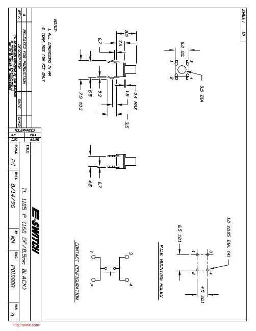
TL1105PF160Q;中文规格书,Datasheet资料
- 格式:pdf
- 大小:36.77 KB
- 文档页数:2
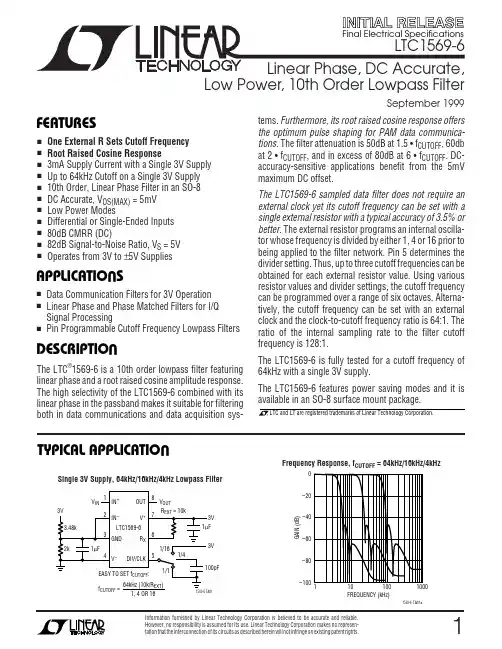
1Information furnished by Linear Technology Corporation is believed to be accurate and reliable.However, no responsibility is assumed for its use. Linear Technology Corporation makes no represen-tation that the interconnection of its circuits as described herein will not infringe on existing patent rights.2LTC1569-6A U G WA W U W A R BSOLUTEXI TI SW U UPACKAGE/ORDER I FOR ATIO(Note 1)Total Supply Voltage................................................11V Power Dissipation..............................................500mW Operating Temperature................................0°C to 70°C Storage Temperature............................–65°C to 150°C Lead Temperature (Soldering, 10 sec)..................300°CThe q denotes the specifications which apply over the full operating temperature range, otherwise specifications are at T A = 25°C.V S = 3V (V + = 3V, V – = 0V), f CUTOFF = 64kHz, R LOAD = 10k unless otherwise specified.ELECTRICAL C C HARA TERISTICSConsult factory for Industrial and Military grade parts.PARAMETER CONDITIONSMIN TYP MAX UNITS Filter GainV S = 5V, f CLK = 4.096MHz,f IN = 1280Hz = 0.02 • f CUTOFF q –0.050.050.15dB f CUTOFF = 64kHz, V IN = 1.4V P-P ,f IN = 12.8kHz = 0.2 • f CUTOFF q –0.25–0.15–0.05dB R EXT = 10k, Pin 5 Shorted to Pin 4f IN = 32kHz = 0.5 • f CUTOFF q –0.65–0.55–0.4dB f IN = 51.2kHz = 0.8 • f CUTOFF q –1.3–1.0–0.7dB f IN = 64kHz = f CUTOFFq –5.3–3.8–2.4dB f IN = 97.5kHz = 1.5 • f CUTOFF q –60–48dB f IN = 128kHz = 2 • f CUTOFF q –62–50dB f IN = 192kHz = 3 • f CUTOFF q –71–60dB V S = 2.7V, f CLK = 1MHz,f IN = 312Hz = 0.02 • f CUTOFF q –0.120.050.16dB f CUTOFF = 15.625kHz, V IN = 1V P-P ,f IN = 3125kHz = 0.2 • f CUTOFF q –0.25–0.15–0.05dB Pin 6 Shorted to Pin 4, External Clockf IN = 7812kHz = 0.5 • f CUTOFF q –0.65–0.55–0.4dB f IN = 12.5kHz = 0.8 • f CUTOFF q –1.1–0.9–0.7dB f IN = 15.625kHz = f CUTOFF q –3.6–3.4–3.2dB f IN = 23.44kHz = 1.5 • f CUTOFF q –54–50dB f IN = 31.25kHz = 2 • f CUTOFF q –60–55dB f IN = 46.88kHz = 3 • f CUTOFF q –66–60dB Filter PhaseV S = 2.7V, f CLK = 4MHz,f IN = 1250Hz = 0.02 • f CUTOFF –11Deg f CUTOFF = 62.5kHz, Pin 6 Shorted to f IN = 12.5kHz = 0.2 • f CUTOFF q –114–111–108Deg Pin 4, External Clockf IN = 31.25kHz = 0.5 • f CUTOFF q 798285Deg f IN = 50kHz = 0.8 • f CUTOFF q –83–79–75Deg f IN = 62.5kHz = f CUTOFFq156162168Deg f IN = 93.75kHz = 1.5 • f CUTOFF–91DegFilter Cutoff Accuracy R EXT = 10.24k from Pin 6 to Pin 7,62.5kHz ±1%when Self-Clocked V S = 3V, Pin 5 Shorted to Pin 4Filter Output DC Swing V S = 3V, Pin 3 = 1.11V2.1V P-P (Note 6)q1.9V P-P V S = 5V, Pin 3 = 2V3.6V P-P q3.2V P-P V S = ±5V, Pin 5 Shorted to Pin 7, R LOAD = 20k8.5V P-P3LTC1569-6The q denotes the specifications which apply over the full operating temperature range, otherwise specifications are at T A = 25°C.V S = 3V (V + = 3V, V – = 0V), f CLK = 4.096MHz, f CUTOFF = 64kHz, R LOAD = 10k unless otherwise specified.ELECTRICAL C C HARA TERISTICSPARAMETER CONDITIONSMIN TYP MAX UNITS Output DC Offset R EXT = 10k, Pin 5 Shorted to Pin 7V S = 3V ±2±5mV (Note 2)V S = 5V ±6±12mV V S = ±5V ±15mV Output DC Offset DriftR EXT = 10k, Pin 5 Shorted to Pin 7V S = 3V 25µV/°C V S = 5V 25µV/°C V S = ±5V 75µV/°CClock Pin Logic Thresholds V S = 3V Min Logical “1” 2.7V when Clocked ExternallyMax Logical “0”0.5V V S = 5V Min Logical “1” 4.0V Max Logical “0”0.5V V S = ±5VMin Logical “1” 4.0V Max Logical “0”0.5VPower Supply Current f CLK = 256kHz (40k from Pin 6 to Pin 7,V S = 3V34mA (Note 3)Pin 5 Open, ÷ 4), f CUTOFF = 4kHzq5mA V S = 5V3.55mA q6mA V S = 10V4.57mA q8mA f CLK = 4.096MHz (10k from Pin 6 to Pin 7,V S = 3V 8mA Pin 5 Shorted to Pin 4, ÷ 1), f CUTOFF = 64kHzq11mA V S = 5V9mA q13mA V S = 10V12mA q17mA Clock Feedthrough Pin 5 Open0.1mV RMS Wideband Noise Noise BW = DC to 2 • f CUTOFF 95µV RMSTHDf IN = 3kHz, 1.5V P-P , f CUTOFF = 32kHz80dBClock-to-Cutoff 64Frequency Ratio Max Clock Frequency V S = 3V 5MHz (Note 4)V S = 5V 5MHz V S = ±5V7MHz Min Clock Frequency V S = 3V, 5V, T A < 85°C 1.5kHz (Note 5)V S = ±5V3kHz Input Frequency RangeAliased Components <–65dB 0.9 • f CLKHzNote 1: Absolute maximum ratings are those values beyond which the life of a device may be impaired.Note 2: DC offset is measured with respect to Pin 3.Note 3: If the internal oscillator is used as the clock source and the divide-by-4 or divide-by-16 mode is enabled, the supply current is reduced as much as 40% relative to the divide-by-1 mode.Note 4: The maximum clock frequency is arbitrarily defined as thefrequency at which the filter AC response exhibits >1dB of gain peaking.Note 5: The minimum clock frequency is arbitrarily defined as the frequecy at which the filter DC offset changes by more than 5mV.Note 6: For more details refer to the Input and Output Voltage Range paragraph in the Applications Information section.4LTC1569-6TYPICAL PERFOR A CE CHARACTERISTICSU WTHD vs Input VoltageTHD vs Input FrequencyINPUT VOLTAGE (V P-P )0.51.0 1.52.0 2.53.0 3.54.0T H D (d B )1569-6 G02–50–55–60–65–70–75–80–85–90INPUT FREQUENCY (kHz)51015202530TH D (d B )1569-6 G01–60–65–70–75–80–85–90PI FU CTIO SU U UIN +/IN – (Pins 1, 2): Signals can be applied to either or both input pins. The DC gain from IN + (Pin 1) to OUT (Pin␣8) is 1.0, and the DC gain from Pin 2 to Pin 8 is –1. The input range, input resistance and output range are de-scribed in the Applications Information section. Input voltages which exceed the power supply voltages should be avoided. Transients will not cause latchup if the current into/out of the input pins is limited to 20mA.GND (Pin 3): The GND pin is the reference voltage for the filter and should be externally biased to 2V (1.11V) to maximize the dynamic range of the filter in applications using a single 5V (3V) supply. For single supply operation,the GND pin should be bypassed with a quality 1µF ceramic capacitor to V – (Pin 4). The impedance of the circuit biasing the GND pin should be less than 2k Ω as the GND pin generates a small amount of AC and DC current.For dual supply operation, connect Pin␣3 to a high quality DC ground. A ground plane should be used. A poor ground will increase DC offset, clock feedthrough, noise and distortion.V –/V + (Pins 4, 7): For 3V, 5V and ±5V applications a quality 1µF ceramic bypass capacitor is required from V +(Pin 7) to V – (Pin 4) to provide the transient energy for the internal clock drivers. The bypass should be as close aspossible to the IC. In dual supply applications (Pin 3 is grounded), an additional 0.1µF bypass from V + (Pin 7) to GND (Pin 3) and V – (Pin 4) to GND (Pin 3) is recom-mended.The maximum voltage difference between GND (Pin 3) and V + (Pin 7) should not exceed 5.5V.DIV/CLK (Pin 5): DIV/CLK serves two functions. When the internal oscillator is enabled, DIV/CLK can be used to engage an internal divider. The internal divider is set to 1:1when DIV/CLK is shorted to V – (Pin 4). The internal divider is set to 4:1 when DIV/CLK is allowed to float (a 100pF bypass to V – is recommended). The internal divider is set to 16:1 when DIV/CLK is shorted to V + (Pin 7). In the divide-by-4 and divide-by-16 modes the power supply current is reduced by as much as 40%.When the internal oscillator is disabled (R X shorted to V –) DIV/CLK becomes an input pin for applying an external clock signal. For proper filter operation, the clock waveform should be a squarewave with a duty cycle as close as possible to 50% and CMOS voltages levels (see Electrical Characteristics section for voltage levels). DIV/CLK pin voltages which exceed the power supply voltages should be avoided. Transients will not cause latchup if the fault current into/out of the DIV/CLK pin is limited to 40mA.LTC1569-656LTC1569-6Table1. f CUTOFF vs R EXT , V S = 3V, T A = 25°C, Divide-by-1 ModeR EXT Typical f CUTOFFTypical Variation of f CUTOFF3844Ω*N/A ±3.0%5010Ω*N/A ±2.5%10k 64kHz ±1%20.18k 32kHz ±2.0%40.2k16kHz±3.5%*REXT values less than 10k can be used only in the divide-by-16 mode.In the divide-by-4 and divide-by-16 modes, the cutoff frequencies in Table 1 will be lowered by 4 and 16respectively. When the LTC1569-6 is in the divide-by-4APPLICATIO S I FOR ATIO W UU U and divide-by-16 modes the power is automatically re-duced. This results in up to a 40% power savings with a single 5V supply.The power reduction in the divide-by-4 and divide-by-16modes, however, effects the fundamental oscillator fre-quency. Hence, the effective divide ratio will be slightly different from 4:1 or 16:1 depending on V S , T A and R EXT .Typically this error is less than 1% (Figures 4 and 6).The cutoff frequency is easily estimated from the equation in Figure 1. Examples 1 and 2 illustrate how to use the graphs in Figures 2 through 7 to get a more precise estimate of the cutoff frequency.Figure 4. Typical Divide Ratio in the Divide-by-4 Mode, T A = 25°CFigure 5. Filter Cutoff vs Temperature,Divide-by-4 Mode, R EXT = 10kFigure 3. Filter Cutoff vs Temperature,Divide-by-1 Mode, R EXT = 10kFigure 2. Filter Cutoff vs V SUPPLY ,Divide-by-1 Mode, T A = 25°CV SUPPLY (V)2D I V I D E R A T I O1569-6 F044.084.044.003.9646810TEMPERATURE (°C)–50N O R M A L I Z E D F I L T E R C U T O F F1569-6 F051.0101.0081.0061.0041.0021.0000.9980.9960.9940.9920.990–250255075100V SUPPLY (V)2N O R M A L I Z E D F I L T E R C U T O F F1569-6 F021.041.031.021.011.000.990.980.970.9646810TEMPERATURE (°C)–50N O R M A L I Z E D F I L T E R C U T O F F1569-6 F031.0101.0081.0061.0041.0021.0000.9980.9960.9940.9920.990–250255075100LTC1569-678LTC1569-6When driven with a complementary signal whose com-mon mode voltage is GND, the IN + input appears to have 125k to GND and the IN – input appears to have –125k to GND. To make the effective IN – impedance 125k when driven differentially, place a 62.5k resistor from IN – to GND. For other cutoff frequencies use 62.5k • (128kHz/f CUTOFF ), as shown in the Typical Applications section. The typical variation in dynamic input impedance for a given clock frequency is ±10%.Wideband NoiseThe wideband noise of the filter is the RMS value of the device’s output noise spectral density. The wideband noise data is used to determine the operating signal-to-noise at a given distortion level. The wideband noise is nearly independent of the value of the clock frequency and excludes the clock feedthrough. Most of the wideband noise is concentrated in the filter passband and cannot be removed with post filtering (Table 2). Table 3 lists the typical wideband noise for each supply.Table 2. Wideband Noise vs Supply Voltage, Single 3V SupplyBandwidth Total Integrated NoiseDC to f CUTOFF 80µV RMS DC to 2 • f CUTOFF 95µV RMS DC to f CLK110µV RMSTable 3. Wideband Noise vs Supply Voltage, f CUTOFF = 64kHzTotal Integrated Noise Power Supply DC to 2 • f CUTOFF3V 95µV RMS 5V 100µV RMS ±5V105µV RMSClock FeedthroughClock feedthrough is defined as the RMS value of the clock frequency and its harmonics that are present at the filter’s OUT pin (Pin 8). The clock feedthrough is measured with IN + and IN – (Pins 1 and 2) grounded and depends on the PC board layout and the power supply decoupling. Table␣4shows the clock feedthrough (the RMS sum of the first 11harmonics) when the LTC1569-7 is self-clocked with R EXT = 10k, DIV/CLK (Pin 5) open (divide-by-4 mode). The clock feedthrough can be reduced with a simple RC post filter.APPLICATIO S I FOR ATIO W UU U it reaches the typical limits V MAX and V MIN . The above voltage swings are for R LOAD = 10k for V S = 3V and 5V.R LOAD = 20k for V S = ±5V.To maximize the undistorted peak-to-peak signal swing of the filter, the GND (Pin 3) voltage should be set to 2V (1.11V) in single 5V (3V) supply applications.The LTC1569-6 can be driven with a single-ended or differential signal. When driven differentially, the voltage between IN + and IN – (Pin 1 and Pin 2) is filtered with a DC gain of 1. The single-ended output voltage OUT (Pin 8) is referenced to the voltage of the GND (Pin 3). The common mode voltage of IN + and IN – can be any voltage that keeps the input signals within the power supply range.For noninverting single-ended applications, connect IN –to GND or to a quiet DC reference voltage and apply the input signal to IN +. If the input is DC coupled then the DC gain from IN + to OUT will be 1. This is true given IN + and OUT are referenced to the same voltage, i.e., GND, V – or some other DC reference. To achieve the distortion levels shown in the Typical Performance Characteristics the input signal at IN + should be centered around the DC voltage at IN –. The input can also be AC coupled, as shown in the Typical Applications section.For inverting single-ended filtering, connect IN + to GND or to quiet DC reference voltage. Apply the signal to IN –. The DC gain from IN – to OUT is –1, assuming IN – is referenced to IN + and OUT is reference to GND.Refer to the Typical Performance Characteristics section to estimate the THD for a given input level.Dynamic Input ImpedanceThe unique input sampling structure of the LTC1569-6 has a dynamic input impedance which depends on the con-figuration, i.e., differential or single-ended, and the clock frequency. The equivalent circuit in Figure 8 illustrates the input impedance when the cutoff frequency is 64kHz. For other cutoff frequencies replace the 125k value with 125k • (64kHz/f CUTOFF ).When driven with a single-ended signal into IN – with IN +tied to GND, the input impedance is very high (~10M Ω).When driven with a single-ended signal into IN + with IN –tied to GND, the input impedance is a 125k resistor to GND.LTC1569-6910LTC1569-6Single 3V Operation, AC Coupled Input,64kHz Cutoff Frequencyf CUTOFF =n = 1, 4, 16 FOR PIN 5 ATGROUND, OPEN, V +64kHz n = 1()10k R EXT()n = 1, 4, 16 FOR PIN 5 ATGROUND, OPEN, V+n = 4R EXTSingle 3V Supply Operation, DC Coupled,16kHz Cutoff FrequencySingle 5V Operation, 50kHz Cutoff Frequency,DC Coupled Differential Inputs with Balanced Input Impedancef CUTOFF ~n = 1, 4, 16 FOR PIN 5 ATGROUND, OPEN, V +64kHz n = 1()10k 12.8k()µF±5V Supply Operation, DC Coupled Filter with External Clock SourceTYPICAL APPLICATIO SUFREQUENCY (Hz)G A I N (d B )GROUP DELAY 1569-6 TA02a0–10–20–30–40–50–60–70–80–90µs µsµs Single 3V, AC Coupled Input,64kHz Cutoff FrequencyLTC1569-61112LTC1569-6© Linear Technology Corporation1630 McCarthy Blvd., Milpitas, CA 95035-7417(408) 432-1900 q FAX : (408) 434-0507 q PART NUMBER DESCRIPTIONCOMMENTSLTC1064-3Linear Phase, Bessel 8th Order Filter f CLK /f CUTOFF = 75/1 or 150/1, Very Low Noise LTC1064-7Linear Phase, 8th Order Lowpass Filter f CLK /f CUTOFF = 50/1 or 100/1, f CUTOFF(MAX) = 100kHzLTC1068-x Universal, 8th Order Filterf CLK /f CUTOFF = 25/1, 50/1, 100/1 or 200/1, f CUTOFF(MAX) = 200kHz LTC1069-7Linear Phase, 8th Order Lowpass Filter f CLK /f CUTOFF = 25/1, f CUTOFF(MAX) = 200kHz, SO-8LTC1164-7Low Power, Linear Phase Lowpass Filter f CLK /f CUTOFF = 50/1 or 100/1, I S = 2.5mA, V S = 5V LTC1264-7Linear Phase, 8th Order Lowpass Filter f CLK /f CUTOFF = 25/1 or 50/1, f CUTOFF(MAX) = 200kHz LTC1562/LTC1562-2Universal, 8th Order Active RC Filterf CUTOFF(MAX) = 150kHz (LTC1562)f CUTOFF(MAX) = 300kHz (LTC1562-2)RELATED PARTSFf CUTOFF =n = 1, 4, 16 FOR PIN 5 ATGROUND, OPEN, V +n = 4()R EXT()Single 5V Supply Operation, DC Coupled Input,16kHz Cutoff Frequency0.5V /D I VINPUT 32ksps (OR 64kbps)1569-6 TA07TYPICAL APPLICATIO SU。