inverter[1]
- 格式:pdf
- 大小:381.89 KB
- 文档页数:46


专利名称:INVERTER发明人:KORSSELL, Thomas 申请号:EP04749049.5申请日:20040623公开号:EP1645025A1公开日:20060412专利内容由知识产权出版社提供摘要:The present invention relates to an inverter and a method for converting direct current voltage to alternating current. The inverter comprises a first input arranged to be connected to the ordinary current supply system of a vessel, where the current supply system comprises a generator connected to a battery, and an output, and an output arranged to be connected to an alternating current motor, where, for at least a period of time, the alternating current motor requires a first torque M1 in order to rotate. The inverter comprises, in addition, a regulating circuit arranged to measure a charging current from the generator to the battery and to measure the voltage level in the battery. The regulating circuit is, in addition, arranged to permit a certain output current from the vessel's ordinary current supply system to the inverter which is higher than the charging current, in a first operating mode. The regulating circuit is, in addition, arranged to limit the output current while maintaining the torque for the alternating current motor, in a second operating mode.申请人:Dometic Sweden AB地址:Torggatan 8 171 54 Solna SE国籍:SE代理机构:Wennborg, Johan 更多信息请下载全文后查看。

INVERTER原理简介Inverter 原理简介一、Inverter 的作用Inverter 是一种将DC 转换为AC的器件,用于点亮Panel 背光灯管,其启动瞬间输出约1.1KV- 1.5KV的高压,使冷阴极灯管中的水银蒸发,两电极导通,产生电子,轰击氖气体,产生中子,再轰击水银气体产生紫外线,最后打在荧光粉上而发光,为图像的显示提供背光,正常工作后输出电压约为600V左右,工作电流约在6mA左右。
二、Inverter的基本组成Inverter主要由电压调节器(降压式斩波器)、自激振荡器(多为Royer振荡器)、脉宽调节器PWM IC组成。
INVERTER 基本架构(PWM IC:TL5001)三、电压调节器(降压式斩波器)用于调节供给自激振荡器的电压,从而调节Panel 背光的亮度。
Vo_Von/offR1++L1Vo Vd_输出电压为:V o=Vin*D=Vin*Ton/T(D :负占空比; T on :Q3导通的时间; T :PWM 方波的周期时间)因T 一定,故输出电压V o 与导通时间成正比。
四、 PWM IC (TL5001为例)a.TL5001各脚简要说明PIN1:OUTPUT (输出占空比可调的方波) PIN5:SCP (短路保护)PIN2:VCC (IC 供电) PIN6:DTC (占空比限制)PIN3:COMP (比较器输出) PIN7:RT (振荡器外接电阻)PIN4:FB (反馈) PIN8:GNDTL5001内部结构图Q2TL5001的工作波形五、自激振荡器它是将DC 转换为AC 高压的主要部件。
Vc2Ib1Ib2Vc1Ic1Ic2C1、C2是镇流电容,它使输出电流不会随灯管负载变化而变化很大。
R1、R2作为振荡器的启动电阻,由于晶体管Q1、Q2的特性不同,假设Q1先导通,Ic1慢慢上升(T1的第8脚的电动势为正,Q1维持导通状态,第7脚电动势为负,使Q2截止),上升至Q1完全饱和,此时Ic1不再变化,T1磁通变化量为零,使Q1截止, 产生反向电动势使Q2导通,Ic2慢慢上升,重复上述过程。
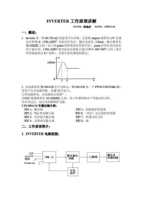
INVERTER工作原理讲解FAOM:林益庆DATE:APR15-02一、概述:1.Inverter是一种DC TO AC的逆变升压回路,它是将adapter提供的12V直流电压转换成1500-1800V交流高压电压,输出电流在5-9mA,输出频率在30-50KHZ之间(以上因panel的特性的差异而不同),panel灯管在高压的作用下被点亮,1500-1800V的交流电压持续1-2S后降至400-700V之间(设计时环境温度以0℃为准),其电压变化曲线如图示:2. 该电路采用TL5001CD芯片为核心,TL5001CD是一个PWM CONTORL IC,常用于开关电源回路,该IC特点如下:①单电源供电,且电源电压范围广。
②OSC振荡频率在20-500KHZ之间,其工作频率取决于外接定时元件。
③具有过压、低压及短路保护功能。
3.TL5001CD引脚功能介绍:PIN 1:输出端PIN 5:短路保护控制端PIN 2:Vcc供电输入端PIN 6:(死区)过压保护控制端PIN 3:误差放大输出端PIN 7:外接定时元件PIN 4:反馈电压输入端PIN 8:地二、工作原理简介:1.INVERTER电路框图:2.电源电压控制电路:如下图这是个常用的电源控制回路,由一个PNP和一个NPN管组成:当ON/OFF电压为高电平(3V)时,Q1管饱和导通,Q2管B极为低电平,因Q2为PNP管故Q2导通,12V 电压加至IC供电脚,启动IC工作;当ON/OFF电压为0时,则INVERTER不工作。
注:ON/OFF电压由MAIN BOARD 提供。
3.稳压回路及过压保护回路:①当IC的Pin2端加上电压(12V)后,IC开始起振、工作,从Pin1脚输出脉冲控制信号,Q4,Q5组成互挽推动放大电路,脉冲控制信号经放大后去驱动Q3管工作,使其工作于开关状态,L1为储能元件,Q3与L1组成降压回路。
L1的输出电压Ul=(T-T OFF)/T ×12V.②输出电压(高压)控制:INVERTER输出电压的大小取决于Dimming电压,通过调节Dimming电压同参考电压比较,来控制Pin1输出脉冲宽度的大小,来决定U L端电压的大小——改变LC振荡回路的供电,从而实现控制INVERTER输出电压电流的大小。
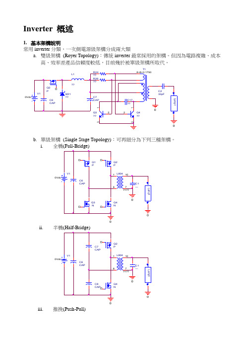
Inverter 概述1. 基本架構說明常用inverter 分類,一次側電源級架構分成兩大類a. 雙級架構 (Royer Topology):傳統inverter 最常採用的架構。
但因為電路複雜、成本高、效率差產品信賴度較低,目前幾於被單級架構所取代。
T1b. 單級架構 (Single Stage Topology):可再細分為下列三種架構。
i. 全橋(Full-Bridge)ii. 半橋(Half-Bridge)iii. 推挽(Push-Pull)根據應用條件的差異設計工程師會選用不同的架構來符合需求的規格、成本及特性。
2.基本比較現行inverter二次側輸出級常用的架構:a.並聯型i.無平衡對策:優點:電路簡單。
缺點:效率差、平衡差、產品較無一致性。
ii.有平衡對策:優點:效率較前述電路好、平衡好且產品一致產高,共用性也較好。
缺點:電路較前述複雜且成本稍高(因為多一個平衡變壓器)。
b.串聯型i.無變壓器電壓考量設計:如下圖示,當Va及Vb均無負載(燈管)時,Va與Vb同為Vkick-off(點燈電壓),此時因為Va與Vb相位為反相(相差180度)則變壓器二次側兩輸出端點的壓差為Vab=(+Va) - (-Vb) 。
假設燈管要求點燈電壓為1800Vrms, 則此時根據前述論點變壓器兩端點的壓差Vab=3600Vrms. 即變壓器必須選用高於3600Vrms 規格的耐壓。
從元件使用的角度來看這樣的設計,並不是一個良好的設計。
因為耐壓高於3600Vrms 以上的變壓器並不容易取得,或是價錢很高。
市面上有一些這類設計的產品,實際上都無法在規格上達要求而退而求其次的希望產品在使用上不要出問題就好。
這種祈求神明保佑的心態原則上應該不能出現在產品設計的概念中。
ii.有變壓器電壓考量設計:如下圖示,當變壓器二次側輸出端均無負載(燈管)時,兩個端點會輸出高壓。
今假設燈管需要1800Vrms 的點燈電壓。

专利名称:INVERTER发明人:HANIWARA KOJI 申请号:JP11006986申请日:19860514公开号:JPS62265752A 公开日:19871118专利内容由知识产权出版社提供摘要:PURPOSE:To simplify a process by forming a protective film between a metal gate and a gate insulating film in an MOSFET having positive threshold voltage, and eliminating a protective film in an MOSFET having negative threshold voltage to differentiate the threshold voltages without varying the impurity distribution of the channel of the FETs. CONSTITUTION:Since a protective film 5 for preventing a metal film from damaging at the time of forming the film is interposed directly under the metal gate electrode of an enhancement FET in case of N-channel type, large boundary level in an Si-SiO2 boundary is suppressed. Since the metal gate electrode 3 of a depression FET is formed thereunder directly with a gate oxide film 4, a large boundary level is generated at the Si-SiO2 boundary, a positive carrier is trapped to shift a threshold voltage in a negative direction. Thus, even if the impurity distribution of the channel part is the same, the threshold voltages of the enhancement and depression FETs can be differentiated to each other.申请人:PIONEER ELECTRONIC CORP更多信息请下载全文后查看。
专利名称:INVERTER发明人:KNAUP, Peter,GONSKA, Gernot 申请号:EP2007062956申请日:20071128公开号:WO09/068092P1公开日:20090604专利内容由知识产权出版社提供摘要:The present invention provides an inverter or other electronically controlled power source for transforming electrical energy into electrical energy of predetermined voltage and/or current comprising: an inner housing (22) for housing the main circuitry of the inverter, a cover (2) connected to the inner housing, covering at least part of the inner housing, defining at least one cover channel (28) between the inner housing and the cover for air to flow through that channel for cooling of the inverter, whereby the cover channel is adapted to facilitate natural convection of the air. The present invention further proposes an inverter according to any of the preceding claims, additionally comprising at least one ventilator to enhance an air flow through the channel. According to the invention the cooling properties of an inverter are to be improved.申请人:KNAUP, Peter,GONSKA, Gernot地址:DE,DE,DE国籍:DE,DE,DE代理机构:SCHÖLING, Ingo更多信息请下载全文后查看。
专利名称:INVERTER发明人:ICHIJIYOU MASAMI,KURITA SHIGEFUMI 申请号:JP4155179申请日:19790407公开号:JPS55136878A公开日:19801025专利内容由知识产权出版社提供摘要:PURPOSE:To obtain high-frequency outputs having high voltages and large currents by a simple control method, by connecting a capacitor to the input side of a self-exciting inverter, and charging said capacitor from a DC power supply of a separately excited inverter. CONSTITUTION:A capacitor 16 is connected to the DC input side of a voltage-type three-phase self-exciting inverter 10. While a DC power supply 22, whose voltage can be adjusted, and a reactor 24 are serially connected to the input side of a current-type three-phase separately excited inverter 18. Then, the outputs of the inverters 10 and 18 are connected by a coupling reactor 26, and a load 28 is connected to the output terminal of the inverter 10. Therefore, the capacitor 16 charged by the DC power supply 22 of the separately excited inverter 18 via the self-exciting inverter 10 at the time of starting, and a specified reverse-bias voltage for commutation can be supplied to the separately excited inverter 18, thereby the number of parts can be reduced, and the high-frequency outputs having high voltages and large currents can be obtained.申请人:FUJI ELECTRIC CO LTD更多信息请下载全文后查看。
专利名称:INVERTER发明人:JIYON HOFUMAN KATORAA,ROOREN HAINESU UOOKAA申请号:JP5365280申请日:19800424公开号:JPS561795A公开日:19810109专利内容由知识产权出版社提供摘要:A fixed gating sequence apparatus and method for an inverter is disclosed. In one aspect of the invention, an outgoing signal of variable frequency is generated by the inverter in response to gating signals provided by an inverter control. The gating signals effectively are provided by a shift register of an inverter control to the gates of the conduction controlled rectifying devices in the inverter in response to a clocking signal. The clocking signal is provided to the clock input of the shift register at a normal system rate when an idle condition (idle control signal) is not present and at a predetermined cycling rate from when the idle condition occurs until a desired fixed gating pattern effectively is provided by the shift register to the inverter. The shift register remains at the stage providing the desired fixed gating pattern until the idle condition no longer is present, whereupon the normal clocking signals are again provided to the shift register. In another aspect, the gating signals, which effectively are normally supplied to the conduction controlled rectifying devices of the inverter, are blocked or inhibited from when the idle condition occurs until the desired fixed gating pattern is provided by the shift register of the control stage of the inverter. Thus, in this aspect, the inverter does not produce a moderate frequency burst of outgoing signal when the shift registercycles through and stops at the desired fixed gating pattern.申请人:GEN ELECTRIC更多信息请下载全文后查看。
Inverter工作原理介绍2007-10-22 09:47Inverter-即逆变器,又叫电压升压板。
它是专为Panel的背光灯提供工作电源的。
Panel使用的背光灯管的工作电压很高,正常工作时的电压为600~800V,而启动电压则高达1500~1800V,工作电流则为5~9mA。
这样的工作特点需要Inverter有如下功能:1)、能够产生1500V以上的高压交流电,并且在短时间内迅速降至800V左右,这段时间约持续1-2S。
2)、由于Inverter提供电流的大小将影响冷阴极荧光灯管的使用寿命,因此输出的电流应小于9mA,需要有过流保护功能。
3)、出于使用的考虑,要有控制功能,即在显示暗画面的时候,灯管不亮。
Inverter是一种DC TO AC的变压器,它其实与Adapter是一种电压逆变的过程。
Adapter是将市电电网的交流电压转变为稳定的12V直流输出,而Inverter 是将Adapter输出的12V直流电压转变为高频的高压交流电;两个部分同样都采用了目前用得比较多的脉宽调制(PWM)技术。
其核心部分都是一个PWM集成控制器,Adapter用的是UC3842,Inverter则采用TL5001芯片。
TL5001的工作电压范围3.6~40V,其内部设有一个误差放大器,一个调节器、振荡器、有死区控制的PWM发生器、低压保护回路及短路保护回路等。
以下将对Inverter的工作原理进行简要介绍:Inverter工作原理框图输入接口部分:输入部分有3个信号,12V直流输入VIN、工作使能电压ENB及Panel电流控制信号DIM。
VIN由Adapter提供,ENB电压由主板上的MCU提供,其值为0或3V,当ENB=0时,Inverter不工作,而ENB=3V时,Inverter处于正常工作状态;而DIM电压由主板提供,其变化范围在0~5V之间,将不同的DIM值反馈给PWM控制器反馈端,Inverter向负载提供的电流也将不同,DIM值越小,Inverter输出的电流就越大。
Chapter 4DC to AC Conversion(INVERTER)•General concept•Single-phase inverter•Harmonics•Modulation•Three-phase inverterPower Electronics and 1DC to AC Converter (Inverter)•DEFINITION: Converts DC to AC power by switching the DC input voltage (or current)in apre-determined sequence so as to generate ACvoltage (or current) output.•General block diagram•TYPICAL APPLICATIONS:–Un-interruptible power supply (UPS), Industrial(induction motor) drives, Traction, HVDCPower Electronics and 2Simple square-wave inverter (1)•To illustrate the concept of AC waveform generationS3S2Power Electronics and 3Power Electronics and 4AC Waveform GenerationVV S3V v tS1,S2 ON; S3,S4 OFFfor t 1 < t < t 2-V tS3,S4 ON ; S1,S2 OFFfor t 2 < t < t 3S2Power Electronics and 5AC WaveformsFUNDAMENTAL COMPONENT3RD HARMONIC5RDHARMONICV-V dcV 131V 51VPower Electronics and 6Harmonics Filtering•Output of the inverter is “chopped AC voltage with zero DC component”. It contain harmonics.•An LC section low-pass filter is normally fitted at the inverter output to reduce the high frequency harmonics.•In some applications such as UPS, “high purity ” sine wave output is required. Good filtering is a must.•In some applications such as AC motor drive, filtering is not required.v O 1v O 2BEFORE FILTERING AFTER FILTERING INVERTERLOADDC SUPPLYVariable Voltage VariableFrequency Capabilityt•Output voltage frequency can be varied by “period”of the square-wave pulse.•Output voltage amplitude can be varied by varying the “magnitude” of the DC input voltage.•Very useful: e.g. variable speed induction motor drivePower Electronics and 7Output voltage harmonics/distortion•Harmonics cause distortion on the output voltage.•Lower order harmonics (3rd, 5th etc) are very difficult to filter, due to the filter size and high filter order. They can cause serious voltage distortion.•Why need to consider harmonics?–Sinusoidal waveform quality must match TNBsupply.–“Power Quality” issue.–Harmonics may cause degradation ofequipment. Equipment need to be “de-rated”.•Total Harmonic Distortion (THD) is a measure to determine the “quality” of a given waveform.Power Electronics and 8Power Electronics and 9Total Harmonics Distortion (THD)()()()()frequency.harmonic at impedance the is :THD Current known,is vaveform for the voltage rms the If .... voltage,harmonic th the is If :THD Voltage ,122,,122,12,12,22,32,2,122,n nn n RMS n RMS n RMSn RMS RMS RMSRMS RMS RMS RMS n RMS n n Z Z V I I I THDi V V V THDv V V V V V V THDv n V ==−=+++== ∞=∞=∞=Power Electronics and 10Fourier Series•Study of harmonics requires understanding of wave shapes. Fourier Series is a tool to analyse wave shapes.()()()tn b n a a v f d n v f b d n v f a d v f a n n n o n n o ωθθθθθπθθπθππππ=++==== ∞= where sin cos 21)(FourierInverse term) sin"(" sin )(1term) cos"(" cos )(1term) DC"(" )(1Series Fourier 1202020Power Electronics and11Harmonics of square-wave (1)()()()()−== −== −+= πππππππππθθθθπθθθθπθθπ202020sin sin 0cos cos 01d n d n V b d n d n V a d V d V a dc n dcn dc dco V dc-V dcθ ωPower Electronics and 12Harmonics of square wave (2)()()[][][][]ππππππππππππθθππππn V b n b n n n n V n n n V n n n n V n n n V b dc n n dcdcdcdc n 41cos odd, is n When exist)not do harmonics even i.e.(01cos even, is When )cos 1(2)cos 1()cos 1()cos 2(cos )cos 0(cos cos cos Solving,20==−==−=−+−=−+−=+−=Spectra of square waven•Spectra (harmonics) characteristics:–Harmonic decreases with a factor of (1/n).–Even harmonics are absent–Nearest harmonics is the 3rd. If fundamental is50Hz, then nearest harmonic is 150Hz.–Due to the small separation between thefundamental an harmonics, output low-passfilter design can be very difficult.Power Electronics and 13Power Electronics and 14Quasi-square wave (QSW)()[]()()[]()()()[]()[]παπαπαπαπαπαπαπαπαπαπθπθθπαπααπαn n n V n n n n V b n n n n n n n n n n n n V n n V d n V b a dc dcn dcdc dc n n cos 1cos 2cos cos cos 2cos cos sin sin cos cos cos cos :Expanding cos cos 2cos 2sin 12symmetry) wave -half to (due .0 that Note −=−= =+=−=−−−=−= ==−−V dc-V dcPower Electronics and 15Harmonics control()()nn b b Note V b n n V b b odcdcn n o31190:if eliminated be will harmonic general,In waveform. the from eliminated is harmonic third or the ,0then ,30 if example For :n Eliminatio Harmonics , adjusting by controlled be also can Harmonics by varying controlled is ,, l fundamenta The :cos 4:is l fundamenta the of amplitude ,particular In cos 4 odd, is n If ,0 even, is n If ===== = ααααπαπPower Electronics and 16Exampledegrees30with case wave square -quasi for (c) and (b)Repeat harmonicszero -non e first thre the using by THDi the c)harmonics zero -non e first thre the using by THDv the b)formula.exact"" the using THDv the a):Calculate series.in 10mH L and 10R R is load The 100V. is ge link volta DC The signals. wave square by fed is inverter phase single bridge -full A ===αPower Electronics and 17Half-bridge inverter (1)V 2Vdc 2Vdc −S1 ON S2 OFFS1 OFF S2 ONt•Also known as the “inverter leg”.•Basic building block for full bridge, three phase and higher order inverters.•G is the “centre point”.•Both capacitors have the same value. Thus the DC link is equally “spilt” into two.•The top and bottom switch has to be“complementary”, i.e. If the top switch is closed (on), the bottom must be off, and vice-versa.Power Electronics and 18Shoot through fault and“Dead-time”•In practical, a dead time as shown below is required to avoid “shoot-through” faults, i.e. short circuit across the DC rail.•Dead time creates “low frequency envelope”. Low frequency harmonics emerged.•This is the main source of distortion for high-qualitysine wave inverter.t dt d"Dead time' = t dS 1signal (gate)S 2signal (gate)+−V dc"Shoot through fault" .I short is very largePower Electronics and 19Single-phase, full-bridge (1)•Full bridge (single phase) is built from two half-bridge leg.•The switching in the second leg is “delayed by 180 degrees” from the first leg.S2dcV V −tttV G R o V V V RG '−=groumd"virtual " is G LEG R LEG R'dcV +-Three-phase inverter•Each leg (Red, Yellow, Blue) is delayed by 120 degrees.• A three-phase inverter with star connected load is shown belowBBPower Electronics and 20Power Electronics and 21132,423,54354,641,56512,661,32Inverter PhaseVoltage (or pole switchingwaveform)V RGIntervalPositive device(s) on Negative device(s) on2V DC V DC -V DC /3-2V DC V -V V DC /2-V DC/2Quasi-square wave operation voltage waveformsV DC /2V DC /2-V DC -V DC /2V YGV BGlIne-to -ine Voltage V RYSix-step Waveform V RNPulse Width Modulation (PWM)•Triangulation method (Natural sampling)–Amplitudes of the triangular wave (carrier) andsine wave (modulating) are compared to obtainPWM waveform. Simple analogue comparatorcan be used.–Basically an analogue method. Its digitalversion, known as REGULAR sampling iswidely used in industry.Power Electronics and 22PWM types •Natural (sinusoidal) sampling (as shown on previous slide)–Problems with analogue circuitry, e.g. Drift,sensitivity etc.•Regular sampling–simplified version of natural sampling thatresults in simple digital implementation •Optimised PWM–PWM waveform are constructed based oncertain performance criteria, e.g. THD.•Harmonic elimination/minimisation PWM –PWM waveforms are constructed to eliminatesome undesirable harmonics from the outputwaveform spectra.–Highly mathematical in nature•Space-vector modulation (SVM)– A simple technique based on volt-second that isnormally used with three-phase inverter motor-drivePower Electronics and 23Power Electronics and 24waveformmodulating the of Frequency veformcarrier wa the of Frequency M )(M Ratio) (Frequency Ratio Modulation veform carrier wa the of Amplitude waveform modulating the of Amplitude M :M Depth)n (Modulatio Index Modulation R R I I ======p pPower Electronics and 25()(1,2,3...)integer an is and signal modulating the of frequency the is where M :at located normally are harmonics The spectra.in the harmonics of (location)incident the determines ratio dulation M ly.respective voltage,(DC)input and voltage output the of l fundamenta are , where M 1, M 0 If component l fundamenta voltage output the s deterrmine Index Modulation R 1I 1I k f f k f o V V V V m m in in=−−−−−−−−−−−−−−−−−−−−−−−−−−−−=<<Power Electronics and 26Regular samplingRegular sampling PWMttvAsymmetric and symmetricregular sampling−Generating of PWM waveform regular samplingPower Electronics and 27Power Electronics and 28Power Electronics and 29Unipolar switching schemeABCarrier waveform (a)(b)(c)(d)1S 3S pwmVBipolar PWM switching: Pulse-width characterizationPower Electronics and 30The k th PulseThekthPWMpulsePower Electronics and 31Power Electronics and 32Determination of switching anglesfor kth PWM pulse (1)2211second,- volt the Equating p s p s A A A A ==Power Electronics and 33PWM Switching angles (2)()()()()()()()()[])sin(2Similarly,)sin(sin 2 cos )2cos(sin sinusoid, by the supplied second - volt The 222half, second for the Similarly 222:as given is pulse PWM the of cycle half first the during second -Volt The 22122221111o k m o s o k o m k o k m m s o k dc k o dc k dc p o k dc k o dc k dc p V A V V d V A V V V A V V V A kok δαδδαδαδαθθδδδδδδδδδδαδα+=−=−−==−=− − =−=− − = −Power Electronics and 34Switching angles (3)()()()()[])sin(1:by given is waveform PWM the of cycle half first for the width pulse the Thus,modulation as known is 2Ratio, Modulation the ,definition By sin(2)sin(2pulse,PWM of cycle half first the for the Hence, ;strategy, modulation the derive To )sin(2)sin(2,sin angle small For 111221121o k I o k dc mI o k o dc mo k o k m o o k dc s p s p o k m o s o k m o s o o oM )(V V M V V V V A A A A V A V A δαδδδαδδδδαδδδδαδδαδδδδ−+= =−=− −=−==−= −= →Power Electronics and 35PWM switching angles (4)[][]k I o k kk o k I o k kk M M αδδδδδδδδαδαδδδαsin 1 Hence,Modulation Symmetric For different. are and i.e ,Modulation Asymmetric for valid is equation above The : angle edge trailing the And )sin(1: waveform PWM of cycle half second the of width pulse method,similar Using :is pulse kth the of angle switching edge leading the Thus k2k 1k 2k 1k 221+= ==+++=−Power Electronics and 36Example•For the PWM shown below, calculate the switching angles pulses no. 2.5.12πPower Electronics and37−+ + −== +++−−−o k k k k k k k k k o k d n V d n V d n V d n v f b dc dc dc T nk δαδαδαδαδαδαθθπθθπθθπθθπ2202211sin 22sin 22sin 22sin )(12:as computed be can pulse PWM (kth) each of content harmonic symmetry, wave half is waveform PWM the AssumingPower Electronics and 38{}[]equation. this of n computatio the shows slide Next :i.e. period, one over pulses for the of sum isthe waveform PWM for the coefficent Fourier ly.The productivesimplified be cannot equation This 2cos cos 2 )2(cos )(cos 2Yeilding,)2(cos )(cos )(cos )(cos )(cos )2(cos :to reduced be can Which 1112121 ==+−−−=+−++−−++−−−−=pk nkn nk o k k k k k dcnk o k k k k k k k k k o k dcnk b b p b n n n n n V b n n n n n n n V b δααδαπδαδαδαδαδαδαπPower Electronics and 39PWM Spectra2.0=I M Fundamental.0.0.0.0.1NORMALISED HARMONIC AMPLITUDES FOR SINUSOIDAL PULSE-WITDH MODULATIONPWM spectra observations•The harmonics appear in “clusters” at multiple of the carrier frequencies .•Main harmonics located at :f = kp(f m);k=1,2,3....where f m is the frequency of the modulation (sine)waveform.•There also exist “side-bands” around the main harmonic frequencies.•Amplitude of the fundamental is proportional to the modulation index.The relation ship is given as:V1= M I V in•The amplitude of the harmonic changes with M I.Its incidence (location on spectra) is not.•When p>10, or so, the harmonics can benormalised. For lower values of p, the side-bandsclusters overlap-normalised results no longer apply.Power Electronics and 40Tabulated Bipolar PWM HarmonicsPower Electronics and 41Three-phase harmonics•For three-phase inverters, there is significant advantage if M R is chosen to be:–Odd: All even harmonic will be eliminatedfrom the pole-switching waveform.–triplens(multiple of three (e.g. 3,9,15,21, 27..):All triplens harmonics will be eliminated fromthe line-to-line output voltage.•By observing the waveform, it can be seen that with odd M R, the line-to-line voltage shape looks more“sinusoidal”.•As can be noted from the spectra, the phase voltage amplitude is 0.8 (normalised). This is because themodulation index is 0.8. The line voltage amplitude is square root three of phase voltage due to thethree-phase relationshipPower Electronics and 42Power Electronics and 43Effect of odd and “triplens”2dc V 2dcV −2dc V 2dcV −2dcV −2dcV −2dc V 2dcV dcV dcV dcV −dc V −ππ2RGV RGV RYV RYV YGV YGV 6.0,8==M p 6.0,9==M p ILLUSTRATION OF BENEFITS OF USING A FREQUENCY RATIO THAT IS A MULTIPLE OF THREE IN A THREE PHASE INVERTERPower Electronics and 44Spectra: effect of “triplens”.0.0.0.0.1.1.1.1.1COMPARISON OF INVERTER PHASE VOLTAGE (A) & INVERTER LINE VOLTAGE (B) HARMONIC (P=21, M=0.8)BComments on PWM schemeas large as possible.•It is desirable to have MR•This will push the harmonic at higher frequencies on the spectrum. Thus filtering requirement isreduced.•Although the voltage THD improvement is not significant, but the current THD will improvegreatly because the load normally has some current filtering effect.has side effects:•However, higher MR–Higher switching frequency: More losses.–Pulse width may be too small to be constructed.“Pulse dropping” may be required.Power Electronics and 45Power Electronics and 46Example Harmonicnumber Amplitude (pole switching waveform)Amplitude (line-to line voltage)11190.3210.8230.3370.1390.2410.25430.25450.2470.1570.05590.1610.15630.2650.15670.1690.05The amplitudes of the pole switching waveform harmonics of the red phase of a three-phase inverter is shown in Table below. The inverter uses a symmetric regular sampling PWM scheme. The carrier frequency is 1050Hz and the modulating frequency is 50Hz. The modulation index is 0.8. Calculate the harmonic amplitudes of the line-to-voltage (i.e. red to blue phase) and complete the table.。