400W大功率稳压逆变器电路浅析
- 格式:doc
- 大小:3.22 KB
- 文档页数:1

逆变器的电路图及维修简要随着绿色能源可再生能源的大规模开发和利用,太阳能凭借其独特的优点得到了更多的关注。
太阳能是当前世界上最清洁、最现实、大规模开发利用最有前景的可再生能源之一。
其中太阳能光伏利用受到世界各国的普遍关注,而太阳能光伏并网发电是太阳能光伏利用的主要发展趋势,必将得到快速的发展。
本论文就是在此背景下,对太阳能并网发电系统中最大功率跟踪控制技术、并网控制策略、孤岛效应检测方法等进行了研究,具有重要的现实意义。
太阳能光伏并网发电系统的两个核心部分是太阳能电池板的最大功率点跟踪(MPPT)控制和光伏并网逆变控制。
本文重点对光伏发电的逆变器最大功率点跟踪技术、孤岛检测技术以及光伏电站并网控制技术进行了讨论,并且预测了光伏发电技术的发展趋势。
1研究背景传统电能的生产百分之六七十都采用的火电形式,火电是用煤发电,有大量的温室气体和有毒气体产生,这些气体的排放破坏生态平衡,并且全球各国工业对煤、石油、天然气等化石能源的需求量急剧增长,而这些不可再生能源的储量是有限的,越来越少,不该作为燃料耗尽。
太阳能具有分布广泛,资源可再生,易采集,清洁、干净、污染小,建造灵活方便,扩容方便,具有通用性,有可存储性等特点。
太阳能系统可以加入蓄电池储存电能,光伏建筑集成,把太阳能光伏发电系统直接与建筑物相结合,这样能节省发电站使用的土地面积、减少了传输成本。
最后太阳能光伏具有分布式特点,光伏发电系统的分布式特点既可以提高整个能源系统的安全可靠性,特别是从抵御自然灾害和战备的角度看,更具有明显的意义。
2光伏并网发电系统的基本介绍2.1光伏并网发电系统的基本原理太阳能光伏发电并网系统是将太阳能光伏阵列发出的直流电转化为与公共电网电压同频同相的交流电,因此该系统是既能满足本地负载用电又能向公共电网送电。
一般情况下,公共电网系统可看作是容量为无穷大的交流电压源。
当太阳能光伏发电并网系统中太阳能光伏阵列的发电量小于本地负载用电量时,本地负载电力不足部分由公共电网输送供给;当光伏电池阵列的发电量大于本地负载用电量时,太阳能光伏系统将多余的电能输送给公共电网,实现并网发电。

逆变器(inverter)是把直流电能(电池、蓄电瓶)转变成交流电(一般为220v50HZ正弦或方波)。
应急电源,一般是把直流电瓶逆变成220V交流的。
通俗的讲,逆变器是一种将直流电(DC)转化为交流电(AC)的装置。
它由逆变桥、控制逻辑和滤波电路组成.利用TL494组成的400W大功率稳压逆变器电路。
它激式变换部分采用TL494,VT1、VT2、VD3、VD4构成灌电流驱动电路,驱动两路各两只60V/30A的MOS FET开关管。
如需提高输出功率,每路可采用3~4只开关管并联应用,电路不变。
TL494在该逆变器中的应用方法如下:第1、2脚构成稳压取样、误差放大系统,正相输入端1脚输入逆变器次级取样绕组整流输出的15V直流电压,经R1、R2分压,使第1脚在逆变器正常工作时有近4.7~5.6V取样电压。
反相输入端2脚输入5V基准电压(由14脚输出)。
当输出电压降低时,1脚电压降低,误差放大器输出低电平,通过PWM电路使输出电压升高。
正常时1脚电压值为5.4V,2脚电压值为5V,3脚电压值为0.06V。
此时输出AC电压为235V(方波电压)。
第4脚外接R6、R4、C2设定死区时间。
正常电压值为0.01V。
第5、6脚外接CT、RT设定振荡器三角波频率为100Hz。
正常时5脚电压值为1.75V,6脚电压值为3.73V。
第7脚为共地。
第8、11脚为内部驱动输出三极管集电极,第12脚为TL494前级供电端,此三端通过开关S控制TL494的启动/停止,作为逆变器的控制开关。
当S1关断时,TL494无输出脉冲,因此开关管VT4~VT6无任何电流。
S1接通时,此三脚电压值为蓄电池的正极电压。
第9、10脚为内部驱动级三极管发射极,输出两路时序不同的正脉冲。
正常时电压值为1.8V。
第13、14、15脚其中14脚输出5V基准电压,使13脚有5V高电平,控制门电路,触发器输出两路驱动脉冲,用于推挽开关电路。
第15脚外接5V电压,构成误差放大器反相输入基准电压,以使同相输入端16脚构成高电平保护输入端。
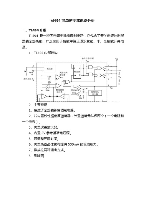
tl494简单逆变器电路分析一、TL494介绍TL494是一种固定频率脉宽调制电路,它包含了开关电源控制所需的全部功能,广泛应用于桥式单端正激双管式、半、全桥式开关电源。
1、TL494内部结构2、主要特征1、集成了全部的脉宽调制电路。
2、片内置线性锯齿波振荡器,外置振荡元件仅两个(一个电阻和一个电容)。
3、内置误差放大器。
4、内置5V参考基准电压源。
5、可调整死区时间。
6、内置功率晶体管可提供500mA的驱动能力。
7、推或拉两种输出方式。
3、引脚图二、经典tl494逆变应用1、应用一这个算是最简单的应用了:屏蔽了两个误差放大器的功能,但缓启动,死区功能还是保留的。
一般应用效率最高,非常稳定。
1:按手册要求两个误差放大器屏蔽的话要求误差放大器输入端正极要求接地(图中1脚和16脚通过1K的电阻接地了),误差放大器输入端负极要求接高电位(2脚和15脚是接入了14脚的5V基准端了)。
注意下TL494的14脚是个5V输出的精密稳压电源,好多应用都是从这个基准端取样的。
这样TL494的1脚2脚15脚16脚再加上3脚(3脚是两个误差放大器的输出汇总端,因为屏蔽了两个误差放大器就不去考虑3脚了)的功能就不去用它了。
2:TL494的4脚是死区控制端,电压输入0-4V的话可使占空比从最大到关闭是为止(45%-0%).4脚直接接地的话占空比是最大了(不过放心厂家已经在集成电路内部做好了合适的死区电路,4脚就是直接接地也留有死区)。
在上图种就是利用4脚接入C1和R1的中间,电容正极接14脚的5V基准电位,通过R1给电容充电,这样开机后4脚开始是5V的电位到电容充满电后4脚变0V(真好完成占空比从0%到最大)整个缓启动的时间长短就C1和R1的时间常数决定(加大电阻或电容缓启动时间变长反之就短了)。
3:5脚6脚是决定振荡频率的,公式是F=1.1/(R*C)注意下整个频率算出来是单端应用的频率,如果推挽应用的话还要除以二。
这里一起把TL494单端应用和推挽应用的方式也讲下:TL494的13脚决定了工作方式,13脚接地的话是单端应用如果接14脚5V输出端就是推挽应用了。

采用TL494的400W大功率稳压逆变器电路采用TL494的400W大功率稳压逆变器电路笔者曾用过300W逆变器,利用12V/60AH蓄电池向上述家用电器供电,一次充满电后,可使用近5小时。
标称功率300W的逆变电源,用于家庭电风扇、电视机,以及日常照明等是不成问题的。
不过,即使蓄电池电压充足,启动180立升的电冰箱仍有困难,因启动瞬间输出电压下降为不足180V而失败。
电冰箱压缩机标称功率多为100W 左右,实际启动瞬间电流可达2A以上,若欲使启动瞬间降压不十分明显,必须将输出功率提高至600VA。
如在增大输出功率的同时,采用PWM稳压系统,可使启动瞬间降压幅度明显减小。
无论电风扇还是电冰箱,应用逆变电源供电时,均应在逆变器输出端增设图1中的LC滤波器,以改善波形,避免脉冲上升沿尖峰击穿电机绕组。
采用双极型开关管的逆变器,基极驱动电流基本上为开关电流的1/β,因此大电流开关电路必须采用多级放大,不仅使电路复杂化,可靠性也变差而且随着输出功率的增大,开关管驱动电流需大于集电极电流的1/β,致使普通驱动IC无法直接驱动。
虽说采用多级放大可以达到目的,但是波形失真却明显增大,从而导致开关管的导通/截止损耗也增大。
目前解决大功率逆变电源及UPS的驱动方案,大多采用MOS FET管作开关器件。
一、MOSFET管的应用近年来,金属氧化物绝缘栅场效应管的制造工艺飞速发展,使之漏源极耐压(VDS)达kV以上,漏源极电流(IDS)达50A已不足为奇,因而被广泛用于高频功率放大和开关电路中。
除此而外,还有双极性三极管与MOS FET管的混合产品,即所谓IGBT绝缘栅双极晶体管。
顾名思义,它属MOS FET管作为前级、双极性三极管作为输出的组合器件。
因此,IGBT既有绝缘栅场效应管的电压驱动特性,又有双极性三极管饱合压降小和耐压高的输出特性,其关断时间达到0.4μs以下,VCEO达到1.8kV,ICM达到100A的水平,目前常用于电机变频调速、大功率逆变器和开关电源等电路中。

逆变器电路原理分析逆变器的定义逆变器是通过半导体功率开关的开通和关断作用,把直流电能转变成交流电能的一种变换装置,是整流变换的逆过程。
车载逆变器的整个电路大体上可分为两大部分,每部分各采用一只TL494或KA7500芯片组成控制电路,其中第一部分电路的作用是将汽车电瓶等提供的12V直流电,通过高频PWM (脉宽调制)开关电源技术转换成30kHz-50kHz、220V左右的交流电;第二部分电路的作用则是利用桥式整流、滤波、脉宽调制及开关功率输出等技术,将30kHz~50kHz、220V左右的交流电转换成50Hz、220V的交流电。
高频升压逆变控制电路:(1)脚第一组放大器的同相输入端,检测输出电流,与3个0.33R 电阻分压,当电流过大时,分压电阻上的电压超过(2)脚基准电压,(3)脚放大器输出端输出高电平,(3)脚为高电平时,电路进入保护状态。
(2)脚为比较器的反相输入端,接(14)脚基准,作比较器的参考电压,外部输入端的控制信号可输入至脚(4)的截止时间控制端(也叫死区时间控制),与脚(1)、(2)、(15)、(16)误差放大器的输入端,其输入端点的抵补电压为120mV,其可限制输出截止时间至最小值,大约为最初锯齿波周期时间的4%。
当13脚的输出模控制端接地时,可获得96%最大工作周期,而当(13)脚接制参考电压时,可获得48%最大工作周期。
如果我们在第4脚截止时间控制输入端设定一个固定电压,其范围由0V至3.3V之间,则附加的截止时间一定出现在输出上。
(5)、(6)脚是一个固定频率的脉冲宽度调制电路,内置了线性锯齿波振荡器,振荡频率可通过外部的一个电阻和一个电容进行调节,其振荡频率如下:输出脉冲的宽度是通过电容CT上的正极性锯齿波电压与另外两个控制信号进行比较来实现。
功率输出管Q1和Q2受控于或非门。
当双稳触发器的时钟信号为低电平时才会被选通,即只有在锯齿波电压大于控制信号期间才会被选通。
当控制信号增大,输出脉冲的宽度将减小。

逆变器电路图各图对应讲解齐全逆变器是一种把直流电能(电池、蓄电池)转变成交流电(一般为220伏50HZ正弦波或方波)的装置。
我们常见的应急电源,一般都是把直流电瓶逆变成220V交流的。
简单来讲,逆变器就是一种将直流电转化为交流电的装置。
下面让我们来看看逆变器电路图及相关介绍。
一、逆变器电路图及介绍1、性能优良的家用逆变电源电路图这种设计,材料易取,输出功率150W,本电路设计频率为300HZ左右,目的是缩小逆变变压器的体积、重量、输出波形方波。
这款逆变电源可以用在停电时家庭照明,电子镇流器的日光灯,开关电源的家用电器等其他方面。
这款逆变器较为容易制作,可以将12V 直流电源电压逆变为220V市电电压,电路由BG2和BG3组成的多谐振荡器推动,再通过BG1和BG2驱动,来控制BG6和BG7工作。
其中振荡电路由BG5与DW组的稳压电源供电,这样可以使输出频率比较稳定。
在制作时,变压器可选有常用双12V输出的市电变压器。
可根据需要,选择适当的12V蓄电池容量。
2、高效率的正弦波逆变器电器图该电路用12V电池供电。
先用一片倍压模块倍压为运放供电。
可选取ICL7660或MAX1044。
运放1产生50Hz正弦波作为基准信号。
运放2作为反相器。
运放3和运放4作为迟滞比较器。
其实运放3和开关管1构成的是比例开关电源。
运放4和开关管2也同样。
它的开关频率不稳定。
在运放1输出信号为正相时,运放3和开关管工作。
这时运放2输出的是负相。
这时运放4的正输入端的电位(恒为0)总比负输入端的电位高,所以运放4输出恒为1,开关管关闭。
在运放1输出为负相时,则相反。
这就实现了两开关管交替工作。
当基准信号比检测信号,也即是运放3或4的负输入端的信号比正输入端的信号高一微小值时,比较器输出0,开关管开,随之检测信号迅速提高,当检测信号比基准信号高一微小值时,比较器输出1,开关管关。
这里要注意的是,在电路翻转时比较器有个正反馈过程,这是迟滞比较器的特点。
大功率逆变电源主电路的设计与实现摘要:本文针对大功率逆变电源系统主电路的研究和设计,提出了一种基于PWM控制器件SA4828和51单片机的控制电路,用于产生和调节一系列的控制脉冲来控制逆变开关的导通和关断,从而配合逆变主电路完成逆变功能。
与传统的SPWM技术相比:SA4828可以提供高质量、全数字化的三相脉宽调制波形,并能实现精确控制,以构成性能优异的逆变系统。
用51单片机作为处理器,即能满足系统的控制要求,又降低了成本,系统结构简单,元器件少,成本低且系统更加稳定。
关键词:逆变电源单片机SA48280 引言目前,大功率逆变电源的设计方法不一,控制电路也不相同,但基本上都是基于现代逆变系统的基本结构,通过不同的电路设计,来提高系统的可靠性及抗干扰能力。
本文介绍如何利用PWM控制器件SA4828和51单片机设计控制电路,产生和调节逆变系统所需要的驱动脉冲。
1 逆变系统概述逆变系统是以燃料发电机不稳定的电能输出(即粗电)作为变换对象,经过电力电子变换,变换为满足用电需求的稳定的交流电能输出(即精电)。
逆变系统的核心毋庸置疑是完成逆变功能的逆变电路,此外逆变系统还需要产生和调节驱动脉冲的电路及控制电路,还要有保护电路,辅助电源电路,输入电路和输出电路等。
这些电路构成了逆变系统的基本结构,其系统结构图如图1。
本文主要研究设计控制电路模块。
2 控制电路系统硬件设计控制电路的功能是按要求产生和调节一系列的控制脉冲来控制逆变开关的导通和关断,从而配合逆变主电路完成逆变功能。
在逆变系统中,控制电路和逆变电路同样重要。
整个控制器由微处理器和SPWM发生器组成。
在此采用AT89S51单片机作为主控制器,SPWM波的产生选择了专用集成芯片SA4828,输出采样和TL431精准电压比较。
单片机通过对电压电流的采样,A/D转换为数字量的形式传入单片机,通过适当的算法来控制SA4828的PWM波的输出,达到控制逆变开关的导通和关断的目的。
LM339集成块内部装有四个独立的电压比较器,该电压比较器的特点是:1)失调电压小,典型值为2mV;2)电源电压范围宽,单电源为2-36V,双电源电压为±1V-±18V;3)对比较信号源的内阻限制较宽;4)共模范围很大,为0~(Ucc-1.5V)Vo;5)差动输入电压范围较大,大到可以等于电源电压;6)输出端电位可灵活方便地选用。
LM339集成块采用C-14型封装,图1为外型及管脚排列图。
由于LM339使用灵活,应用广泛,所以世界上各大IC 生产厂、公司竟相推出自己的四比较器,如IR2339、ANI339、SF339等,它们的参数基本一致,可互换使用。
图 1LM339类似于增益不可调的运算放大器。
每个比较器有两个输入端和一个输出端。
两个输入端一个称为同相输入端,用“+”表示,另一个称为反相输入端,用“-”表示。
用作比较两个电压时,任意一个输入端加一个固定电压做参考电压(也称为门限电平,它可选择LM339输入共模范围的任何一点),另一端加一个待比较的信号电压。
当“+”端电压高于“-”端时,输出管截止,相当于输出端开路。
当“-”端电压高于“+”端时,输出管饱和,相当于输出端接低电位。
两个输入端电压差别大于10mV就能确保输出能从一种状态可靠地转换到另一种状态,因此,把LM339用在弱信号检测等场合是比较理想的。
LM339的输出端相当于一只不接集电极电阻的晶体三极管,在使用时输出端到正电源一般须接一只电阻(称为上拉电阻,选3-15K)。
选不同阻值的上拉电阻会影响输出端高电位的值。
因为当输出晶体三极管截止时,它的集电极电压基本上取决于上拉电阻与负载的值。
另外,各比较器的输出端允许连接在一起使用。
单限比较器电路图1a给出了一个基本单限比较器。
输入信号Uin,即待比较电压,它加到同相输入端,在反相输入端接一个参考电压(门限电平)Ur。
当输入电压Uin>Ur时,输出为高电平U OH。
AN983/DA Simplified Power Supply Design Using the TL494Control CircuitPrepared by: Jade H. Alberkrack ON Semiconductor Bipolar IC DivisionThis bulletin describes the operation and characteristics of the TL494 SWITCHMODE t V oltage Regulator and shows its application in a 400–watt off–line power supply.The TL494 is a fixed–frequency pulse width modulation control circuit, incorporating the primary building blocks required for the control of a switching power supply. (See Figure 1). An internal linear sawtooth oscillator is frequency–programmable by two external components, R T and C T . The oscillator frequency is determined by:f osc ^ 1.1R T @C TOutput pulse width modulation is accomplished by comparison of the positive sawtooth waveform across capacitor C T to either of two control signals. The NOR gates,which drive output transistors Q1 and Q2, are enabled only when the flip–flop clock–input line is in low state. Thishappens only during that portion of time when the sawtooth voltage is greater than the control signals. Therefore, an increase in control–signal amplitude causes a corresponding linear decrease of output pulse width. (Refer to the timing diagram shown in Figure 2).The control signals are external inputs that can be fed into the dead–time control (Figure 1, Pin 4), the error amplifier inputs (Pins 1, 2, 15, 16), or the feedback input (Pin 3). The dead–time control comparator has an effective 120 mV input offset which limits the minimum output dead time to approximately the first 4% of the sawtooth–cycle time. This would result in a maximum duty cycle of 96% with the output mode control (Pin 13) grounded, and 48% with it connected to the reference line. Additional dead time may be imposed on the output by setting the dead–time control input to a fixed voltage, ranging between 0 to 3.3 V .Figure 1. TL494 Block DiagramThis document may contain references to devices which are no longer offered. Please contact your ON Semiconductor representative for information on possible replacement devices.APPLICATION NOTEFigure 2. TL494 Timing DiagramCapacitor CFeedback/P The pulse width modulator comparator provides a means for the error amplifiers to adjust the output pulse width from the maximum percent on–time, established by the dead–time control input, down to zero, as the voltage at the feedback pin varies from 0.5 to 3.5 V . Both error amplifiers have a common mode input range from –0.3 V to (V CC –2V), and may be used to sense power supply output voltage and current. The error amplifier outputs are active high and are ORed together at the inverting input of the pulse width modulator comparator. With this configuration, the amplifier that demands minimum output on time, dominates control of the loop.When capacitor C T is discharged, a positive pulse is generated on the output of the dead–time comparator, which clocks the pulse steering flip–flop and inhibits the output transistors, Q1 and Q2. With the output mode control connected to the reference line, the pulse–steering flip–flop directs the modulated pulses to each of the two output transistors alternately for push–pull operation. The output frequency is equal to half that of the oscillator. Output drive can also be taken from Q1 or Q2, when single–ended operation with a maximum on–time of less than 50% is required. This is desirable when the output transformer has a ringback winding with a catch diode used for snubbing.When higher output drive currents are required for single–ended operation, Q1 and Q2 may be connected in parallel, and the output mode control pin must be tied to ground to disable the flip–flop. The output frequency will now be equal to that of the oscillator.The TL494 has an internal 5 V reference capable of sourcing up to 10 mA of load currents for external bias circuits. The reference has an internal accuracy of ±5% witha thermal drift of less than 50 mV over an operating temperature range of 0 to 70°C.APPLICATION OF THE TL494 IN A 400 OFF–LINE POWER SUPPLYA 5 V , 80 A line operated 25 kHz switching power supply,designed around the TL494, is shown in Figure 3, and the performance data is shown in Table 1. A brief explanation of each section of the power supply is as follows:AC Input SectionThe operating ac line voltage is selectable for nominal of 115 or 230 volts by moving the jumper links to their appropriate positions. The input circuit is a full wave voltage doubler when connected for 115 V AC operation with both halves of the bridge connected in parallel for added line–surge capability. When connected for 230 V AC operation, the input circuit forms a standard full wave bridge.The line voltage tolerance for proper operation is –10,+20% of nominal. The ac line inrush current, during power up, is limited by resistor R1. It is shorted out of the circuit by triac Q1, only after capacitors C1 and C2 are fully charged,and the high frequency output transformer T1, commences operation.Power SectionThe high frequency output transformer is driven in a half–bridge configuration by transistors Q3 and Q5. Each transistor is protected from inductive turn–off voltage transients by an R–C snubber and a fast recovery clamp rectifier. Transistors Q2 and Q4 provide turn–off drive to Q3and Q5, respectively. In order to describe the operation of Q2, consider that Q6 and Q3 are turned on. Energy iscoupled from the primary to the secondary of T3, forward biasing the base–emitter of Q3, and charging C3 through CR1. Resistor R3 provides a dc path for the ‘on’ drive after C3 is fully charged. Note that the emitter–base of Q2 is reverse biased during this time. Turn–off drive to Q3 commences during the dead–time period, when both Q6 and Q7 are off. During this time, capacitor C3 will forward bias the base–emitter of Q2 through R3 and R2 causing it to turn on. The base–emitter of Q3 will now be reverse biased by the charge stored in C3 coupled through the collector–emitter of Q2.Output SectionThe ac voltage present at the secondaries of T1 is rectified by four MBR 6035 Schottky devices connected in a full wave center tapped configuration. Each device is protected from excessive switching voltage spikes by an R–C snubber, and output current sharing is aided by having separate secondary windings. Output current limit protection is achieved by incorporating a current sense transformer T4. The out–of–phase secondary halves of T1 are cross connected through the core of T4, forming a 1–turn primary. The 50 kHz output is filtered by inductor L1, and capacitor C4. Resistor R4 is used to guarantee that the power supply will have a minimum output load current of 1 ampere. This prevents the output transistors Q3 and/or Q5 from cycle skipping, as the required on–time to maintain regulation into an open circuit load is less than that of the devices storage time. Transformer T5 is used to reduce output switching spikes by providing common mode noise rejection, and its use is optional.The MC3423, U1, is used to sense an overvoltage condition at the output, and will trigger the crowbar SCR, Q8. The trip voltage is centered at 6.4 V with a programmed delay of 40 m s. In the event that a fault condition has caused the crowbar to fire, a signal is sent to the control section via jumper ‘A’ or ‘B.’ This signal is needed to shut down the output, which will prevent the crowbar SCR from destruction due to over dissipation. Automatic over voltage reset is achieved by connecting jumper ‘A’. The control section will cycle the power supply output every 2 seconds until the fault has cleared. If jumper ‘B’ is connected, SCR Q12 will inhibit the output until the ac line is disconnected. Low Voltage Supply SectionA low current internal power supply is used to keep the control circuitry active and independent from external loading of the output section. Transformer T2, Q9 and CR2 form a simple 14.3 V series pass regulator.Control SectionThe TL494 provides the pulse width modulation control for the power supply. The minimum output dead–time is set to approximately 4% by grounding Pin 4 through R5. The soft start is controlled by C5 and R5. Transistor Q11 is used to discharge C5 and to inhibit the operation of the power supply if a low ac line voltage condition is sensed indirectly by Q10, or the output inhibit line is grounded.Error amplifier 1 and 2 are used for output voltage and current–level sensing, respectively. The inverting inputs of both amplifiers are connected together to a 2.5 V reference derived from Pin 14. By connecting the two inputs together, only one R–C feedback network is needed to set the voltage gain and roll off characteristics for both amplifiers. Remote output voltage sensing capability is provided, and the supply will compensate for a combined total of 0.5 V drop in the power busses to the load. The secondary of the output current sense transformer T4, is terminated into 36 W and peak detected by BR1 and C6. The current limit adjust is set for a maximum output current of 85 amperes.The oscillator frequency is set to 50 kHz by the timing components R T and C T. This results in a 25 kHz two phase output drive signal, when the output mode (Pin 13) is connected to the reference output (Pin 14).Table 1. 400 Watt Switcher Performance DataFigure 3. 400 Watt Switchmode Power SupplyTransformer DataT1Core:Bobbin:Windings:Ferroxcube EC 70–3C8, 0.002″ gap in each legFerroxcube 70PTBPrimary (Q3, Q5):Primary (Q1):Secondary, 4 each:Shield, 2 each:50 turns total, #17 AWG Split wound about secondary.4 turns, #17 AWG.3 turns, #14 AWG Quad Filar wound.Made from soft alloy copper 0.002″ thick.T2Core:Bobbin:Windings:Allegheny Ludlum EI–75–M6, 29 gaugeBobbin Cosmo EI 75Primary, 2 each:Secondary:1000 turns, #36 AWG.200 turns, #24 AWG.T3Core:Windings:Ferroxcube 846 T250–3C8Primary, 2 each:Secondary, 2 each:30 turns, #30 AWG Bifilar wound.12 turns, #20 AWG Bifilar wound.T4Core:Windings:Magnetics Inc. 55059–A2Primary, 2 each:Secondary:1 turn, #14 AWG Quad Filar wound. Taken from secondary to T1.500 turns, #30 AWG.T5Core:Windings:Magnetics Inc. 55071–A2Primary:Secondary:4 turns, #16 AWG Hex Filar wound.4 turns, #16 AWG Hex Filar wound.L1Core:Windings:TDK H7C2 DR 56 x 355 turns, soft alloy copper strap, 0.9″ wide x 0.020″ thick,6 m H.SWITCHMODE is a trademark of Semiconductor Components Industries, LLC.ON Semiconductor and are registered trademarks of Semiconductor Components Industries, LLC (SCILLC). SCILLC reserves the right to make changes without further notice to any products herein. SCILLC makes no warranty, representation or guarantee regarding the suitability of its products for any particular purpose, nor does SCILLC assume any liability arising out of the application or use of any product or circuit, and specifically disclaims any and all liability, including without limitation special, consequential or incidental damages. “Typical” parameters which may be provided in SCILLC data sheets and/or specifications can and do vary in different applications and actual performance may vary over time. All operating parameters, including “Typicals” must be validated for each customer application by customer’s technical experts. SCILLC does not convey any license under its patent rights nor the rights of others.SCILLC products are not designed, intended, or authorized for use as components in systems intended for surgical implant into the body, or other applications intended to support or sustain life, or for any other application in which the failure of the SCILLC product could create a situation where personal injury or death may occur. Should Buyer purchase or use SCILLC products for any such unintended or unauthorized application, Buyer shall indemnify and hold SCILLC and its officers, employees, subsidiaries, affiliates, and distributors harmless against all claims, costs, damages, and expenses, and reasonable attorney fees arising out of, directly or indirectly, any claim of personal injury or death associated with such unintended or unauthorized use, even if such claim alleges that SCILLC was negligent regarding the design or manufacture of the part. SCILLC is an Equal Opportunity/Affirmative Action Employer. PUBLICATION ORDERING INFORMATIONJAPAN: ON Semiconductor, Japan Customer Focus Center2–9–1 Kamimeguro, Meguro–ku, Tokyo, Japan 153–0051Phone: 81–3–5773–3850Email: r14525@。
CCM BOOST PFC电路设计浅析——Xia Jun 2010-8-5抛砖引玉,本文仅以最常用的PFC拓扑来探讨电源设计的合理方法,让电源设计尽可能变得透明,科学和合理,最大限度的提高产品开发效率,降低系统设计风险。
当然由于本人水平有限,思考和总结的东西不见得就一定正确,更多的是从工程的角度激发一下大家的思维,用工程的方法去设计产品,好过用经验的方法设计产品。
很多工程师在产品设计当中都有很多的困惑,电路拓扑我都有所了解,但是如何能够根据客户的需求设计出好的产品?大多数时候我们都是在抄袭和模仿,或者根据IC厂家的典型设计进行简单的更改,我们会设计简单的变压器,电感,会根据经验选择电阻,电容,二极管,MOSFET等器件,我们知其然(因为别人就是这么做的),但不知其所以然(因为缺少科学的工程方法)。
别人的方案不一定适合我们的产品,别人的经验也不一定正确,如果我们不能用工程的方法加以归纳,总结和提炼,那么永远只能跟在别人的后面,差距越来越大。
首先,我们要考虑的是,客户的需求是什么?产品的功率等级?输入范围?输出范围?要满足哪些标准?体积?成本(价格)?效率?开发周期?以小功率等级而论(200W以下),DCM BOOST PFC电路显然更为合适,可以较好的兼顾到指标,体积和成本,MOSFET零电流开通,无需任何辅助电路即可实现软开通,二极管零电流关断,用普通的Ultra-fastrecovery二极管即可基本消除反向恢复问题,由于每一个开关周期中,电感电流都会从零开始,再归于零,没有直流偏置问题,可以用铁氧体磁芯代替昂贵的铁硅铝等粉芯类磁环,降低成本,缩小体积,提高效率,同时IC厂家的解决方案丰富,开发周期短。
如果到了中小功率等级(200W~400W),BCM BOOST PFC电路则更为合适,临界导通模式,既有DCM的优点,又可以克服其一些缺点,同时由于是变频控制,EMI的频谱很宽,单个频率点的能量幅值就小得多(在定频控制中,所有的能量都集中在开关频率的基波,二次谐波,三次谐波等谐波频率点上,所以幅值很大),电磁兼容性设计会更容易解决。
400W大功率稳压逆变器电路浅析
利用TL494组成的400W大功率稳压逆变器电路。
它激式变换部分采用TL494,VT1、VT2、VD3、VD4构成灌电流驱动电路,驱动两路各两只60V/30A的MOS FET开关管。
如需提高输出功率,每路可采用3~4只开关管并联应用,电路不变。
TL494在该逆变器中的应用方法如下:
第1、2脚构成稳压取样、误差放大系统,正相输入端1脚输入逆变器次级取样绕组整流输出的15V直流电压,经R1、R2分压,使第1脚在逆变器正常工作时有近4.7~5.6V取样电压。
反相输入端2脚输入5V基准电压(由14脚输出)。
当输出电压降低时,1脚电压降低,误差放大器输出低电平,通过PWM电路使输出电压升高。
正常时1脚电压值为5.4V,2脚电压值为5V,3脚电压值为0.06V。
此时输出AC电压为235V(方波电压)。
第4脚外接R6、R4、C2设定死区时间。
正常电压值为0.01V。
第5、6脚外接CT、RT设定振荡器三角波频率为100Hz。
正常时5脚电压值为1.75V,6脚电压值为3.73V。
第7脚为共地。
第8、11脚为内部驱动输出三极管集电极,第12脚为TL494前级供电端,此三端通过开关S控制TL494的启动/停止,作为逆变器的控制开关。
当S1关断时,TL494无输出脉冲,因此开关管VT4~VT6无任何电流。
S1接通时,此三脚电压值为蓄电池的正极电压。
第9、10脚为内部驱动级三极管发射极,输出两路时序不同的正脉冲。
正常时电压值为1.8V。
第13、14、15脚其中14脚输出5V基准电压,使13脚有5V高电平,控制门电路,触发器输出两路驱动脉冲,用于推挽开关电路。
第15脚外接5V电压,构成误差放大器反相输入基准电压,以使同相输入端16脚构成高电平保护输入端。
此接法中,当第16脚输入大于5V的高电平时,可通过稳压作用降低输出电压,或关断驱动脉冲而实现保护。
在它激逆变器中输出超压的可能性几乎没有,故该电路中第16脚未用,由电阻R8接地。
该逆变器采用容量为400VA的工频变压器,铁芯采用45×60mm2的硅钢片。
初级绕组采用直径1.2mm的漆包线,两根并绕2×20匝。
次级取样绕组采用0.41mm漆包线绕36匝,中心抽头。
次级绕组按230V计算,采用0.8mm漆包线绕400匝。
开关管VT4~VT6可用60V/30A任何型号的N沟道MOS FET管代替。
VD7可用1N400X系列普通二极管。
该电路几乎不经调试即可正常工作。
当C9正极端电压为12V时,R1可在3.6~4.7kΩ之间选择,或用10kΩ电位器调整,使输出电压为额定值。
如将此逆变器输出功率增大为近600W,为了避免初级电流过大,增大电阻性损耗,宜将蓄电池改用24V,开关管可选用VDS为100V 的大电流MOS FET管。
需注意的是,宁可选用多管并联,而不选用单只IDS大于50A的开关管,其原因是:一则价格较高,二则驱动太困难。
建议选用100V/32A的2SK564,或选用三只2SK906并联应用。
同时,变压器铁芯截面需达到50cm2,按普通电源变压器计算方式算出匝数和线径,或者采用废UPS-600中变压器代用。
如为电冰箱、电风扇供电,请勿忘记加入LC低通滤波器。