sp3232中文资料说明书
- 格式:pdf
- 大小:874.58 KB
- 文档页数:19
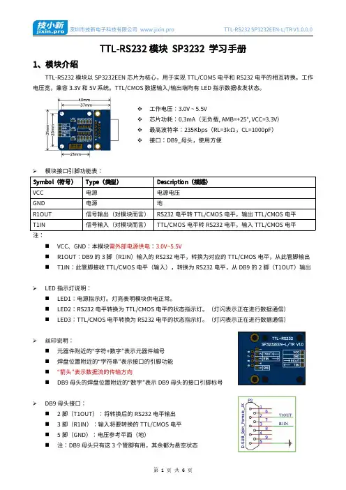
深圳市技新电子科技有限公司www.jixin.pro TTL-RS232SP3232EEN-L/TR V1.0.0.0 TTL-RS232模块SP3232学习手册1、模块介绍TTL-RS232模块以SP3232EEN芯片为核心,用于实现TTL/COMS电平和RS232电平的相互转换。
工作电压宽,兼容3.3V和5V系统。
TTL/CMOS数据输入/输出端均有LED指示数据收发状态。
工作电压:3.0V~5.5V芯片功耗:0.3mA(无负载,AMB=+25°,VCC=3.3V)最高波特率:235Kbps(RL=3kΩ,CL=1000pF)接口:DB9_母头,使用方便模块接口引脚功能表:Symbol(符号)Type(类型)Description(描述)VCC电源电源电压GND电源地R1OUT信号输出(对模块而言)RS232电平转TTL/CMOS电平,输出TTL/CMOS电平T1IN信号输入(对模块而言)TTL/CMOS电平转RS232电平,输入TTL/CMOS电平注:⏹VCC、GND:本模块需外部电源供电:3.0V~5.5V⏹R1OUT:DB9的3脚(R1IN)输入的RS232电平,转换为对应的TTL/CMOS电平,从此管脚输出⏹T1IN:此管脚接收TTL/CMOS电平(输入),转换为RS232电平,从DB9的2脚(T1OUT)输出 LED指示灯说明:⏹LED1:电源指示灯。
灯亮表明模块供电正常。
⏹LED2:RS232电平转换为TTL/CMOS电平的状态指示灯。
(灯闪表示正在进行数据通信)⏹LED3:TTL/CMOS电平转换为RS232电平的状态指示灯。
(灯闪表示正在进行数据通信)丝印说明:⏹元器件附近的“字符+数字”表示元器件编号⏹焊盘位置附近的“字符串”表示接口的引脚功能⏹“箭头”表示数据流的传输方向⏹DB9母头的焊盘位置附近的“数字”表示DB9母头的接口引脚标号DB9母头接口:⏹2脚(T1OUT):将转换后的RS232电平输出⏹3脚(R1IN):输入将要转换的TTL/CMOS电平⏹5脚(GND):电压参考平面(地)⏹注:DB9母头只有这3个管脚有用,其余都为悬空状态深圳市技新电子科技有限公司www.jixin.pro TTL-RS232SP3232EEN-L/TR V1.0.0.0 焊盘C6、C7的作用:⏹C6并联在T1OUT(DB9母头的2脚)和地之间、C7并联在R1IN(DB9母头的3脚)和地之间。
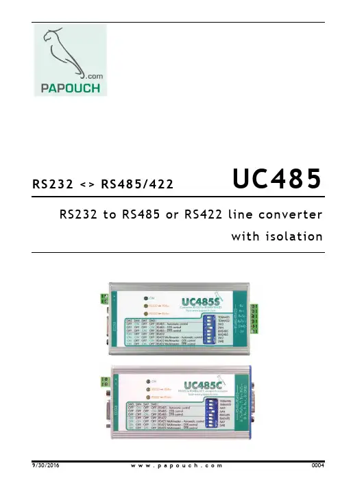
9/30/2016w w w .p a p o u c h .c o m0004RS232 <> RS485/422UC485RS232 to RS485 or RS422 line converterwith isolationUC485 Papouch s.r.o.Page 2U C 485DatasheetCreated: 5/4/2005 Last update: 5/19/2005 9:15Number of pages: 16 © 2016 Papouch s.r.o.P a p o u c h s.r.o.Address:Strasnicka 3164 110 00 Prague 10 Czech RepublicTel:+420 267 314 267Fax:+420 267 314 269Internet:E-mail:****************Papouch s.r.o.UC485Page 3TABLE OF CONTENTSDescription .......................................................... 4 Features ............................................................. 4 Installing options ................................................. 4 Technical Parameters .. (5)General ........................................................ 5 Connector pins ............................................. 5 Settings (6)Modes .......................................................... 6 Line termination and idle mode .................... 7 Automatic control settings ............................ 7 Installation for the RS485/422 line ............... 9 Installation for the RS422 line .................... 11 RS232 line extension ................................. 12 RS485 and RS422 lines .................................... 13 Possible problems during installation . (15)Fig. 1 –Principal diagram of isolationUC485 Papouch s.r.o.Page 4DESCRIPTIONThe UC485 module converts an RS232 line to RS485 or RS422. The module settings can be set with the aid of switches, as described below. The green LED indicates that the module is ON; the yellow indicators show the RxD and TxD status.FEATURES∙Lines can be set: RS485, RS422, and RS422 multimaster∙Transmission speed up to 480 kBd∙Direction control on the RS485 line can be automatic or by DTR signal (whose polarity can be set)∙The RS485/422 line (including the grounding) is completely isolated from RS232 and from the power supply (this isolation is provided as standard for all types) ∙Optionally, grounding of the power supply and grounding of the RS232 line can be isolated from each other∙The RS485/RS422 line is over voltage protected∙The ON and data flow statuses are indicated by LED indicators – the unit activation is easy ∙ A built-in optional termination, including resistors which define the line's idle status∙Power supply 7 to 40 V (depending on the type, also 36 to 75 V or 5 V)∙D-SUB 9 connectors or a slip-on termination board∙Dimensions 105 × 55 × 24 mm, optionally secured to a DIN stripINSTALLING OPTIONSHolder:∙Without a DIN rail holder (standard)∙With a DIN rail holder RS485/422 connection:∙D-SUB 9M (type UC485C)∙Slip-on terminal board (type UC485S)Power supply:∙7 to 40 V 1(standard configuration)∙ 5 V ±10% 1,2∙ 4.5 V ±10% 2,3∙9 V ±10% 2.3∙18 V to 36 V 2.3∙36 V to 75 V 2.3Please do not hesitate to contact us if you have specific requirements for the UC485 module's configuration and functionality.1 The RS485/422 line (including the grounding) is completely conductively separated from RS232 and from thepower supply (G1 separation cf. Fig. 1). The power supply and the RS232 line have common grounding.2 The time limit for delivery of this configuration is between one and three weeks.3 The RS232 line's grounding is conductively separated from the power supply's grounding (cf. Fig. 1 to seethe G2 separation).Fig. 2 – UC485SPapouch s.r.o.UC485Page 5TECHNICAL PARAMETERSG e n e r a lPower supply voltage ........................ 7 V to 40 V (optionally, 4.5 – 75 V) with protection frompolarity reversal Power supply connector .................... S lip-on connector board Isolation ............................................. 1,000 V Maximum transmission speed ........... 480 kBd Operating temperature....................... –20 °C to +70 °C RS485/422:Terminal resistors .............................. 120 Ω Resistors which define the idle status ......... 680 Ω Maximum number of connected devices . (31)Voltage overprotection ....................... y es, 12 V bipolar transil diodes UC485C connection .......................... D -SUB 9MUC485S ............................................. s lip-on connector board RS232:Voltage overprotection ....................... 15 kV Connection ........................................ D -SUB 9M C o n n e c t o r p i n s16Fig. 3 – RS232 pinsFig. 4 - RS485/422 pins on UC485CFig. 5 – Power supply connector Fig. 6 – RS485/422 pins on UC485SUC485 Papouch s.r.o. SETTINGSM o d e sThe communication modes are set by switches on the front panel.Fig. 7 – Front panel switches, module UC485 (they are all OFF in this figure)Table 1 – Settings of the communication line modesPage Papouch s.r.o.UC485Page 7L i n e t e r m i n a t i o n a n d i d l e m o d e TERM485This device connects the impedance termination of the RS485 or RS422 line on the transmitter's side. It prevents signal from reflection at the line ends. These resistors should be connected at both ends of the communication line.TERM422This device connects the impedance termination of the RS422 line on the receiver's side. It prevents signal from reflection at the line ends. These resistors should be connected at both ends of the communication line.BIAS485This device connects the resistors which define the idle mode of the RS485 or RS422 line on the transmitter's side. They determine the idle-status levels of the communication line. (More detailed information can be found in the section "Idle mode" on page 10.)A u t o m a t i c c o n t r o l s e t t i n g sWhen automatic (time) control is used for the RS485 or RS422 line, the value T of the time delay can be set, for which the driver remains switched to transmission.Fig. 8 – Time delay for which the driver remains switched to transmissionThe default value of this delay is 460 μs; it can be changed using jumpers inside of the module. First open the module case. Unscrew the two screws (opposite to each other) on the modulecase's bottom side, loosen the screws on the top lid, and tilt the top lid out.Fig. 9 – Locations of the screws securing the top lidUC485Papouch s.r.o.Page 8There are four jumpers inside.Fig. 10 – Jumpers for setting the time delay valueThe jumpers' configuration defines the time delay value T. The default value of this delay is 460 μs; it can be changed using jumpers inside of the module. The configurations and their meanings are shown in the Table below.Table 2 – Time delay value settingSW1 SW2 SW3 SW4Papouch s.r.o.UC485I n s t a l l a t i o n f o r t h e R S485/422l i n eThe following steps are used for the UC485 converter installation for communication on an RS485 line:1) Set the switches SW3 through SW8 according to Table 1 on page 6.2) Connect the RS485 wires to the D-SUB 9M connector according to Table 3. (Cf. theconnector diagram on page 5.)Table 3 – RS485 line connection3) Connect the RS232 wires to the D-SUB 9F connector according to Table 4 using anuncrossed cable.Table 4 – RS485 line connection4) If the converter is at a line endpoint, the termination resistors should to be connected bya TERM485. Switches consider connection of resistors which define the idle status.5) Connect to the power supply.1The DTR or RTS signal is only used within modes with the DTR line control. The mode settings are described on page 6 under "Modes". Page 9UC485Papouch s.r.o.Page 10Idle modeWhen communicating on the RS485 line or the RS422 multimaster line, there may be a no-transmission status (all lines are in the receiving mode). In this case, the status of the line is undefined and it is extremely sensitive to any induced voltage (interference), which is deemed incoming signals. Therefore an idle mode should be defined by connecting suitable resistors to a line. If the line is long, the best point is at the UC485 end-of-line modules or equipment.With the UC485 converter, built-in resistors can be used, connected by the BIAS485 switches; or the resistors may be connected directly to the RS485 connector (cf. Fig. 11). For long lines, the resistor values should be higher and the termination should be connected simultaneously.SGND can also be used for connection of the cable shielding contact.Fig. 11 – Connection of resistors which define the idle modeI n s t a l l a t i o n f o r t h e R S422l i n eThe following steps are used for the UC485 converter installation for communication between two devices on an RS422 line:1) Set the switches SW3 through SW8 according to Table 1 on page 6.2) Connect the RS422 leads to the D-SUB 9M connector according to Table 5 (a drawing ofthe connectors is on page 5).Table 5 – RS422 line connection3) Connect the RS232 leads to the D-SUB 9F connector according to Table 6 using anuncrossed cable.Table 6 – RS232 line connection4) If the converter is at a line endpoint, the termination resistors are to be connected by theTERM422. For the multimaster mode, consider connection of resistors which define the idle status.5) Connect to the power supply.5The DTR or RTS signal is only used within modes with the DTR line control. The mode settings are described on page 6 under "Modes".R S232l i n e e x t e n s i o nBy using two UC485, you can extend an RS232 line to a distance of up to 1,200 m.61) Connect the RS232 line and the power supply to the UC485 converters on both ends.2) Both converters should be set to the RS422 mode according to the above-mentionedinstructions.3) Connect the cable between the converters according to Table 7 (a drawing of theconnectors is on page 5).Table 7 – RS232 extension line connection6 An RS232 line can also be extended with the aid of a special LD232 set.RS485 AND RS422 LINESAn RS485 line consists of a pair of wires, denoted by symbols RxTx+ and RxTx-7, preferably by a twisted pair. In the idle mode, the RxTx+ wire's potential is more positive than that of RxTx-. The topology is a stem line with short branches. Impedance termination devices should be connected at both ends of the stem line. The RS485 line is a half-duplex bus: data is sent and received on the same wires. Therefore the communication direction must be switched between transmission and receipt.Fig. 12 – An example of a system with an RS485 line interconnection. Termination is connected inModules 1 and 5.The DTR signal of the RS232 line can be used for the direction control, or automatic (time) control can be used.Fig. 13 – An example of a system with an RS422 line interconnection. Termination is connected inboth modules.7 Notation A (for RxTx+) and B (for RxTx–) is sometimes used.Fig. 14 – An example of a system with an RS422 line interconnection in the multimaster mode.An RS422 line consists of two symmetric pairs of conductors. It is duplex line and directly substitutes the RxD and TxD signals of the RS232 lines; one pair is used for data receipt, the other pair for transmission. The transmission conductors are denoted by symbols Tx+ and Tx-; the receipt pair are denoted Rx+ and Rx-. In the idle mode, the + wire’s potential is more positive than the – wire. Impedance terminations are connected to the line endpoints. An RS422 line can have branches; in this case, transmitters must be disconnected –mode Multimaster must be set according Table 1.POSSIBLE PROBLEMS DURING INSTALLATIONRecognising RxTx+ and RxTx- conductors:In the idle mode of an RS485 (RS422) line, the RxTx+ conductor's potential is more positive than that of RxTx-. Before measuring, we must ensure that the equipment at the other endpoint is a transmitter and either idle or sending data with a very low frequency of occurrence. If the polarity of the RxTx+ and RxTx- conductors is correct, the yellow RxD indicator must be on when data is transmitted (test it when the control signal is off and the "positive control signal during transmission" option is set).Even thought the power supply is switched on, the green indicator is off: Make sure that power supply is on, the power supply voltage is accordant with converter installing option and polarity is not reversed.The RxD remains on even if no data is being transmitted:There may be several causes of this defect:–The RxTx+ and RxTx- conductors of the RS485 line may be mutually interchanged.–An impedance termination on the receiver side is connected, but there are no resistors which would define the line's idle mode.The impedance termination is connected to the module. On the opposite side, resistors –are connected which define the line's idle mode. However, the line or one of its wires is broken.Data transmission in industry, line and protocol conversions, RS232/485/422/USB/Ethernet/GPRS/ WiFi, measurement modules, intelligenttemperature sensors, I/O modules, and custom-made electronic applications.Address:Strasnicka 3164110 00 Prague 10Czech RepublicTel:+420 267 314 267Fax:+420 267 314 269Internet:E-mail:****************。
DAM3232继电器控制卡说明书V1.0北京聚英翱翔电子有限责任公司2018年12月目录一、产品特点 (1)二、产品功能 (1)三、产品选型 (1)四、主要参数 (2)五、接口说明 (3)1、引脚说明 (3)六、通讯接线说明 (4)1、RS232接线方式 (4)2、RS485级联接线方式 (5)七、输入输出接线说明 (6)1、继电器接线说明................................................................................错误!未定义书签。
2、无源开关量(干接点)接线示意图................................................错误!未定义书签。
3、有源开关量(PNP型高电平)接线示意图....................................错误!未定义书签。
4、模拟量接线示意图..........................................................................错误!未定义书签。
八、测试软件说明 (8)1、软件下载 (8)2、软件界面 (8)3、通讯测试 (9)九、参数配置 (9)1、设备地址 (9)2、波特率的读取与设置 (10)3、闪开闪断功能及设置 (11)十、开发资料说明 (11)1、通讯协议说明 (11)十、智能自控功能配置说明 (12)十一、开发资料说明 (12)1、通讯协议说明 (12)2、Modbus寄存器说明 (12)3、指令生成说明 (15)4、指令列表 (16)5、指令详解 (18)十二、常见问题与解决方法 (25)十三、技术支持联系方式 (25)一、产品特点●DC12V/24V(默认12V);●继电器输出触点隔离;●485通信光电隔离;●通讯接口支持RS485、RS232、RJ45以太网接口、无线WIFI通讯;●通信波特率:2400,4800,9600,19200,38400(可以通过软件修改,默认9600);●通信协议:支持标准modbus-RTU/TCP/ASCLL协议;●可以设置0-255个设备地址;●具有闪开、闪断功能,可以在指令里边带参数、操作继电器开一段时间自动关闭;●具有频闪功能,可以控制器继电器周期性开关。
串口IO控制器说明书本说明书适合型号:modbus rtu协议串口通信口XYS系列RS232 RS485XYS-3232MT-12V 5A三极管输出XYS-3232MT-24V 5A三极管输出XYS-3232MT-4AD2DA-12V 5A三极管输出4路模拟输入0-10V,2路模拟输出0-10V XYS-3232MT-4AD2DA-24V 5A三极管输出4路模拟输入0-10V,2路模拟输出0-10V XYS-3232MR-12V 5A继电器输出XYS-3232MR-24V 5A继电器输出XYS-3232MR-4AD2DA-12V 5A继电器输出4路模拟输入0-10V,2路模拟输出0-10V XYS-3232MR-4AD2DA-24V 5A继电器输出4路模拟输入0-10V,2路模拟输出0-10V网络通信口XYN系列以太网100M TCP/IPXYN-3232MT-12V 5A三极管输出XYN-3232MT-24V 5A三极管输出XYN-3232MT-4AD2DA-12V 5A三极管输出4路模拟输入0-10V,2路模拟输出0-10V XYN-3232MT-4AD2DA-24V 5A三极管输出4路模拟输入0-10V,2路模拟输出0-10V XYN-3232MR-12V 5A继电器输出XYN-3232MR-24V 5A继电器输出XYN-3232MR-4AD2DA-12V 5A继电器输出4路模拟输入0-10V,2路模拟输出0-10V XYN-3232MR-4AD2DA-24V 5A继电器输出4路模拟输入0-10V,2路模拟输出0-10V命令规则:XYN-3232MT-4AD2DA-24V举例:串口32路开关量输入、32路晶体管输出,4路电压/电流采集、2路电压输出、工作电源24VDC;一、应用领域:工作电源12V ,24V可选,通信可选:RS232/RS485/RS232+RS485/以太网协议支持:modbus RTU 或协议定制,默认:modbus RTU支持软件:组态王力控等组态软件支持昆仑等人机界面提供技术支持:提供调试工具、VB源码工程、C# 源码工程、组态王实例工程工业控制:工业交流电机控制、电源开关控制、步进电机控制、开关量采集等;智能家居:家居电源控制、家电控制、开关状态采集、电动门/床帘控制;节能系统:风机控制、路灯控制、空调控制、设备电源控制等;商业应用:宾馆酒店、商场厂房、网吧、办公、实体店铺监控等;无人值守:通信机房、变电站、水厂、机场、地下管道、矿山设备、安防监控等;二、功能介绍本产品采用32位ARM处理器、数字输入量和数字输出量使用高速磁电隔离及光电耦隔离技术。
- 2 -- 3 -- 4 -- 5 -商标鸣谢SP322II:斯大精密有限公司注意•本书记载的公司名称、商品名称为各公司的商标或注册商标。
•禁止擅自转载本书的部分或全部内容。
•本公司对因根据本书运用本机型的结果所产生的影响,以及因过失而导致的损伤不承担任何责任,敬请谅解。
•虽然本书的内容经过精心编写,以期万全,但如果发现有无法理解的地方、记述错误或遗漏等问题,请与本公司联系。
© 版权所有2016 斯大精密有限公司请妥善保管本书,以便日后使用本产品时可随时取阅。
目 录1.开箱和安装 (1)1-1.开箱 (1)1-2.设置注意事项 (1)2.部件与术语 (2)3.安装 (3)3-1.接口电缆的安装 (3)3-2.电源电缆的连接 (5)3-3.打开电源 (5)3-4.色带盒的安装 (6)3-5.纸张的安装 (8)3-6.安装注意事项 (9)4.操作面板 (10)4-1.各部分的名称与功能 (10)5.规格 (11)6.安全指示 (12)1-2. 设置注意事项1. 请将打印机主机放在水平、稳定的场所。
2. 请将打印机主机放在插座附近,以便需要时可立即拔下电源插头。
3. 请勿放在阳光照射的场所。
4. 请勿放在明火周边或热量聚集的场所。
5. 请勿放在通风不良或灰尘较多的场所。
6. 请勿与复印机、冰箱等发生噪音的电器共用同一插座。
7. 请勿放在潮湿的场所。
8. 请在环境性规格所示的范围内使用。
即使环境温度与湿度处在标准范围内,也请避免出现急剧的使用环境条件的变化。
如下所示为适合打印机使用的环境。
温度动作时: 0℃ 至+50℃保存时: -20℃ 至+70℃湿度动作时: 10% 至 90%(不结露)保存时: 5% 至 95%(不结露)1.开箱和安装1-1.开箱打开打印机的机箱,确认包含了以下所有的附件。
9. 废弃时,请遵守当地的条例或规则。
2.部件与术语用于通过电缆连接各种主计算机。
电源开关用于进行打印机电源的ON/OFF操作。
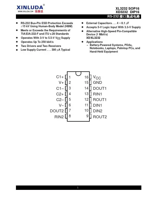
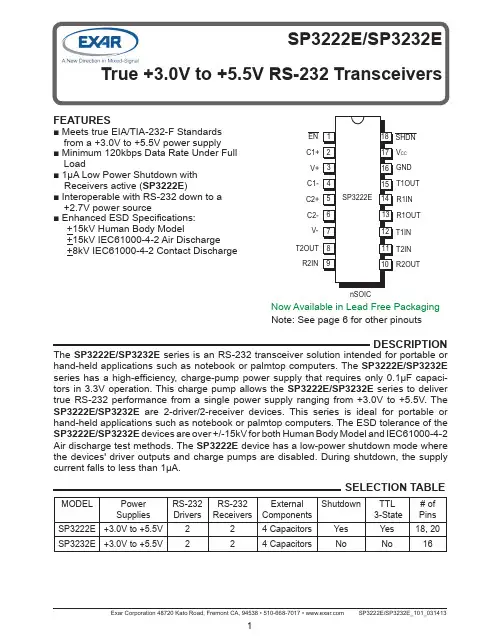
DESCRIPTIONs Meets true EIA/TIA-232-F Standards from a +3.0V to +5.5V power supplys 235KBps Transmission Rate Under Load s 1µA Low-Power Shutdown with Receivers Active (SP3222E )s Interoperable with RS-232 down to +2.7V power sources Enhanced ESD Specifications: ±15kV Human Body Model±15kV IEC1000-4-2 Air Discharge ±8kV IEC1000-4-2 Contact DischargeThe SP3222E/3232E series is an RS-232 transceiver solution intended for portable or hand-held applications such as notebook or palmtop computers. The SP3222E/3232E series has a high-efficiency, charge-pump power supply that requires only 0.1µF capacitors in 3.3V operation. This charge pump allows the SP3222E/3232E series to deliver true RS-232performance from a single power supply ranging from +3.3V to +5.0V. The SP3222E/3232E are 2-driver/2-receiver devices. This series is ideal for portable or hand-held applications such as notebook or palmtop computers. The ESD tolerance of the SP3222E/3232E devices are over ±15kV for both Human Body Model and IEC1000-4-2 Air discharge test methods. The SP3222E device has a low-power shutdown mode where the devices' driver outputs and charge pumps are disabled. During shutdown, the supply current falls to less than 1µA.SELECTION TABLEL E D O M s e i l p p u S r e w o P 232-S R s r D e v i r 232-S R sr e v i e c e R l a n r e t x E st n e n o p m o C nw o d t u h S L T T a S -3e t t f o .o N s n i P 2223P S V 5.5+o t V 0.3+224s e Y s e Y 02,812323P S V5.5+o t V 0.3+224oN oN 61RE T E M A R A P .N I M .P Y T .X A M ST I N U SN O I T I D N O C S C I T S I R E T C A R A H C C D tn e r r u C y l p p u S 3.00.1A m T ,d a o l o n B M A 52+=o V ,C C C V 3.3=tn e r r u C y l p p u S n w o d t u h S 0.101µA,D N G =N D H S T B M A 52+=o V ,C C C V3.3+=S T U P T U O R E V I E C E R D N A S T U P N I C I G O L W O L d l o h s e r h T c i g o L t u p n I 8.0V 2e t o N ,N D H S ,N E ,N I x T H G I H d l o h s e r h T c i g o L t u p n I 0.24.2V V C C 2e t o N ,V 3.3=V C C 2e t o N ,V 0.5=t n e r r u C e g a k a e L t u p n I 10.0±0.1±µA ,N D H S ,N E ,N I x T T B M A 52+=o C t n e r r u C e g a k a e L t u p t u O 50.0±01±µA d e l b a s i d s r e v i e c e r W O L e g a t l o V t u p t u O 4.0V I T U O A m 6.1=H G I H e g a t l o V t u p t u O V C C 6.0-V C C 1.0-VI T U O Am 0.1-=S T U P T U O R E V I R D gn i w S e g a t l o V t u p t u O 0.5±4.5±Vk 3Ω,s t u p t u o r e v i r d l l a t a d n u o r g o t d a o l T B M A 52+=o Cec n a t s i s e R t u p t u O 003ΩV C C T ,V 0=-V =+V =T U O =+V 2t n e r r u C t i u c r i C -t r o h S t u p t u O 53±07±06±001±A m A m V T U O V 0=V T U O =+V51tn e r r u C e g a k a e L t u p t u O 52±µAV T U O =+V ,V 21C C de l b a s i d s r e v i r d ,V 5.5o t V 0=NOTE 1: V+ and V- can have maximum magnitudes of 7V, but their absolute difference cannot exceed 13V.ABSOLUTE MAXIMUM RATINGSThese are stress ratings only and functional operation of the device at these ratings or any other above those indicated in the operation sections of the specifications below is not implied. Exposure to absolute maximum rating conditions for extended periods of time may affect reliability and cause permanent damage to the device.V CC ................................................................-0.3V to +6.0V V+ (NOTE 1)................................................-0.3V to +7.0V V- (NOTE 1)................................................+0.3V to -7.0V V+ + |V-| (NOTE 1)....................................................+13V I CC (DC V CC or GND current).................................±100mAInput VoltagesTxIN, EN .....................................................-0.3V to +6.0V RxIN.............................................................................±25V Output VoltagesTxOUT.....................................................................±13.2V RxOUT..............................................-0.3V to (V CC + 0.3V)Short-Circuit DurationTxOUT...............................................................Continuous Storage Temperature.................................-65°C to +150°C Power Dissipation Per Package20-pin SSOP (derate 9.25mW/o C above +70o C).......750mW 18-pin PDIP (derate 15.2mW/o C above +70o C)......1220mW 18-pin SOIC (derate 15.7mW/o C above +70o C)......1260mW 20-pin TSSOP (derate 11.1mW/o C above +70o C).....890mW 16-pin SSOP (derate 9.69mW/o C above +70o C).......775mW 16-pin PDIP (derate 14.3mW/o C above +70o C)......1150mW 16-pin Wide SOIC (derate 11.2mW/o C above +70o C)....900mW 16-pin TSSOP (derate 10.5mW/o C above +70o C).....850mWSPECIFICATIONSUnless otherwise noted, the following specifications apply for V CC = +3.0V to +5.0V with T AMB = T MIN to T MAXR E T E M A R A P .N I M .P Y T .X A M ST I N U SN O I T I D N O C S T U P N I R E V I E C E R e g n a R e g a t l o V t u p n I 51-51+V W O L d l o h s e r h T t u p n I 6.08.02.15.1V V C C V 3.3=V C C V 0.5=H G I H d l o h s e r h T t u p n I 5.18.14.24.2V V C C V 3.3=V C C V0.5=s i s e r e t s y H t u p n I 3.0V ec n a t s i s e R t u p n I 357k ΩS C I T S I R E T C A R A H C G N I M I T e t a R a t a D m u m i x a M 021532s p b k R L k 3=ΩC ,L g n i h c t i w s r e v i r d e n o ,F p 0001=y a l e D n o i t a g a p o r P r e v i r D 0.10.1µs µs t L H P R ,L K 3=ΩC ,L F p 0001=t H L P R ,L K 3=ΩC ,L F p 0001=y a l e D n o i t a g a p o r P r e v i e c e R 3.03.0µs t L H P C ,T U O x R o t N I x R ,L F p 051=t H L P C ,T U O x R o t N I x R ,L Fp 051=e m i T e l b a n E t u p t u O r e v i e c e R 002s n e m i T e l b a s i D t u p t u O r e v i e c e R 002s n w e k S r e v i r D 001005s n t |L H P t -H L P T ,|B M A 52=o C we k S r e v i e c e R 0020001s n t |L H P t -H L P |et a R w e l S n o i g e R -n o i t i s n a r T 03/V µsV C C R ,V 3.3=L K 3=ΩT ,B M A 52=o ,C V 0.3+o t V 0.3-m o r f n e k a t s t n e m e r u s a e m V0.3-o t V 0.3+r o SPECIFICATIONS (continued)Unless otherwise noted, the following specifications apply for V CC = +3.0V to +5.0V with T AMB = T MIN to T MAX .Typical Values apply at V CC = +3.3V or +5.0V and T AMB = 25o C.NOTE 2: Driver input hysteresis is typically 250mV.Capacitance for the SP3222 and the SP3232SP3222 and the SP3232Transmitting Data for the SP3222 and the SP3232TYPICAL PERFORMANCE CHARACTERISTICSUnless otherwise noted, the following performance characteristics apply for V CC = +3.3V, 235kbps data rates, all drivers loaded with 3k Ω, 0.1µF charge pump capacitors, and T AMB = +25°C.DESCRIPTIONThe SP3222E/3232E transceivers meet the EIA/TIA-232 and V.28/V.24 communication proto-cols and can be implemented in battery-pow-ered, portable, or hand-held applications such as notebook or palmtop computers. The SP3222E/3232E devices all feature Sipex's proprietary on-board charge pump circuitry that generates 2x V CC for RS-232 voltage levels from a single +3.0V to +5.5V power supply. This series is ideal for +3.3V-only systems, mixed +3.3V to +5.5V systems, or +5.0V-only systems that re-quire true RS-232 performance. The SP3222E/3232E series have drivers that operate at a typi-cal data rate of 235Kbps fully loaded.The SP3222E and SP3232E are 2-driver/2-re-ceiver devices ideal for portable or hand-held applications. The SP3222E features a 1µA shutdown mode that reduces power consump-tion and extends battery life in portable systems.Its receivers remain active in shutdown mode,allowing external devices such as modems to be monitored using only 1µA supply current.THEORY OF OPERATIONThe SP3222E/3232E series are made up of three basic circuit blocks: 1. Drivers, 2. Receivers,and 3. the Sipex proprietary charge pump.DriversThe drivers are inverting level transmitters that convert TTL or CMOS logic levels to ±5.0V EIA/TIA-232 levels inverted relative to the in-put logic levels. Typically, the RS-232 output voltage swing is ±5.5V with no load and at least ±5V minimum fully loaded. The driver outputs are protected against infinite short-circuits to ground without degradation in reliability. Driver outputs will meet EIA/TIA-562 levels of ±3.7V with supply voltages as low as 2.7V.The drivers typically can operate at a data rate of 235Kbps. The drivers can guarantee a data rate of 120Kbps fully loaded with 3K Ω in parallel with 1000pF, ensuring compatibility with PC-to-PC communication software.The slew rate of the driver output is internally limited to a maximum of 30V/µs in order to meet the EIA standards (EIA RS-232D 2.1.7, Para-graph 5). The transition of the loaded output from HIGH to LOW also meets the monotonic-ity requirements of the standard.The SP3222E/3232E drivers can maintain high data rates up to 240Kbps fully loaded. Figure 8shows a loopback test circuit used to test the RS-232 drivers. Figure 9 shows the test results of the loopback circuit with all drivers active at 120Kbps with RS-232 loads in parallel with 1000pF capacitors. Figure 10 shows the test results where one driver was active at 235Kbps and all drivers loaded with an RS-232 receiver in parallel with a 1000pF capacitor. A solid RS-232 data transmission rate of 120Kbps provides compatibility with many designs in personal computer peripherals and LAN applications.The SP3222E driver's output stages are turned off (tri-state) when the device is in shutdown mode. When the power is off, the SP3222E device permits the outputs to be driven up to ±12V. The driver's inputs do not have pull-up resistors. Designers should connect unused inputs to V CC or GND.In the shutdown mode, the supply current falls to less than 1µA, where SHDN = LOW. When the SP3222E device is shut down, the device's driver outputs are disabled (tri-stated) and the charge pumps are turned off with V+ pulled down to V CC and V- pulled to GND. The time required to exit shutdown is typically 100µs.Connect SHDN to V CC if the shutdown mode is not used. SHDN has no effect on RxOUT or RxOUTB. As they become active, the two driver outputs go to opposite RS-232 levels where one driver input is HIGH and the other LOW. Note that the drivers are enabled only when the magnitude of V- exceeds approximately 3V.ReceiversThe receivers convert EIA/TIA-232 levels to TTL or CMOS logic output levels. All receivers have an inverting tri-state output. These receiver outputs (RxOUT) are tri-stated when the enable control EN = HIGH. In the shutdown mode, the receivers can be active or inactive. EN has no effect on TxOUT. The truth table logic of the SP3222E/3232E driver and receiver outputs can be found in Table 2.Since receiver input is usually from a transmis-sion line where long cable lengths and system interference can degrade the signal, the inputs have a typical hysteresis margin of 300mV. This ensures that the receiver is virtually immune to noisy transmission lines. Should an input be left unconnected, a 5k Ω pulldown resistor to ground will commit the output of the receiver to a HIGH state.Charge PumpThe charge pump is a Sipex –patented design (5,306,954) and uses a unique approach com-pared to older less–efficient designs. The charge pump still requires four external capacitors, but uses a four–phase voltage shifting technique to attain symmetrical 5.5V power supplies. The internal power supply consists of a regulated dual charge pump that provides output voltages 5.5V regardless of the input voltage (V CC ) over the +3.0V to +5.5V range.In most circumstances, decoupling the power supply can be achieved adequately using a 0.1µF bypass capacitor at C5 (refer to Figures 6 and 7).In applications that are sensitive to power-sup-ply noise, decouple V CC to ground with a capaci-tor of the same value as charge-pump capacitor C1. Physically connect bypass capacitors as close to the IC as possible.The charge pumps operate in a discontinuous mode using an internal oscillator. If the output voltages are less than a magnitude of 5.5V, the charge pumps are enabled. If the output voltage exceed a magnitude of 5.5V, the charge pumps are disabled. This oscillator controls the four phases of the voltage shifting. A description of each phase follows.Phase 1— V SS charge storage — During this phase of the clock cycle, the positive side of capacitors C 1and C 2 are initially charged to V CC . C l + is then switched to GND and the charge in C 1– is trans-ferred to C 2–. Since C 2+ is connected to V CC , the voltage potential across capacitor C 2 is now 2times V CC .Phase 2— V SS transfer — Phase two of the clock con-nects the negative terminal of C 2 to the V SS storage capacitor and the positive terminal of C 2to GND. This transfers a negative generated voltage to C 3. This generated voltage is regu-lated to a minimum voltage of -5.5V. Simulta-neous with the transfer of the voltage to C 3, the positive side of capacitor C 1 is switched to V CC and the negative side is connected to GND.Phase 3— V DD charge storage — The third phase of the clock is identical to the first phase — the charge transferred in C 1 produces –V CC in the negative terminal of C 1, which is applied to the negative side of capacitor C 2. Since C 2+ is at V CC , the voltage potential across C 2 is 2 times V CC .Table 2. Truth Table Logic for Shutdown and Enable ControlN D H S N E T U O x T T U O x R 00e t a t s -i r T e v i t c A 01e t a t s -i r T e t a t s -i r T 10e v i t c A e v i t c A 11ev i t c A et a t s -i r TPhase 4— V DD transfer — The fourth phase of the clock connects the negative terminal of C 2 to GND,and transfers this positive generated voltage across C 2 to C 4, the V DD storage capacitor. This voltage is regulated to +5.5V. At this voltage,the internal oscillator is disabled. Simultaneous with the transfer of the voltage to C 4, the positive side of capacitor C 1 is switched to V CC and the negative side is connected to GND, allowing the charge pump cycle to begin again. The charge pump cycle will continue as long as the opera-tional conditions for the internal oscillator are present.Since both V + and V – are separately generated from V CC ; in a no–load condition V + and V – will be symmetrical. Older charge pump approaches that generate V – from V + will show a decrease in the magnitude of V – compared to V + due to the inherent inefficiencies in the design.The clock rate for the charge pump typically operates at 250kHz. The external capacitors can be as low as 0.1µF with a 16V breakdown voltage rating.ESD ToleranceThe SP3222E/3232E series incorporates ruggedized ESD cells on all driver output and receiver input pins. The ESD structure is improved over our previous family for more rugged applications and environments sensitive to electro-static discharges and associated transients. The improved ESD tolerance is at least ±15kV without damage nor latch-up.There are different methods of ESD testing applied:a) MIL-STD-883, Method 3015.7b) IEC1000-4-2 Air-Discharge c) IEC1000-4-2 Direct Contact The Human Body Model has been the generally accepted ESD testing method for semiconduc-tors. This method is also specified in MIL-STD-883, Method 3015.7 for ESD testing. The premise of this ESD test is to simulate the human body’spotential to store electro-static energy and discharge it to an integrated circuit. The simulation is performed by using a test model as shown in Figure 17. This method will test the IC’s capability to withstand an ESD transient during normal handling such as in manufacturing areas where the ICs tend to be handled frequently.The IEC-1000-4-2, formerly IEC801-2, is generally used for testing ESD on equipment and systems. For system manufacturers, they must guarantee a certain amount of ESD protection since the system itself is exposed to the outside environment and human presence.The premise with IEC1000-4-2 is that the system is required to withstand an amount of static electricity when ESD is applied to points and surfaces of the equipment that are accessible to personnel during normal usage.The transceiver IC receives most of the ESD current when the ESD source is applied to the connector pins. The test circuit for IEC1000-4-2is shown on Figure 18. There are two methods within IEC1000-4-2, the Air Discharge method and the Contact Discharge method.With the Air Discharge Method, an ESD voltage is applied to the equipment under test (EUT) through air. This simulates an electrically charged person ready to connect a cable onto the rear of the system only to find an unpleasant zap just before the person touches the back panel. The high energy potential on the person discharges through an arcing path to the rear panel of the system before he or she even touches the system. This energy, whether discharged directly or through air, is predominantly a function of the discharge current rather than the discharge voltage.Variables with an air discharge such as approach speed of the object carrying the ESD potential to the system and humidity will tend to change the discharge current. For example, the rise time of the discharge current varies with the approach speed.Figure 14. Charge Pump WaveformsThe Contact Discharge Method applies the ESD current directly to the EUT. This method was devised to reduce the unpredictability of the ESD arc. The discharge current rise time is constant since the energy is directly transferred without the air-gap arc. In situations such as hand held systems, the ESD charge can be directly discharged to the equipment from a person already holding the equipment. The current is transferred on to the keypad or the serial port of the equipment directly and then travels through the PCB and finally to the IC.The circuit models in Figures 17 and 18 represent the typical ESD testing circuits used for all three methods. The C S is initially charged with the DC power supply when the first switch (SW1) is on. Now that the capacitor is charged, the second switch (SW2) is on while SW1 switches off. The voltage stored in the capacitor is then applied through R S, the current limiting resistor, onto the device under test (DUT). In ESD tests, the SW2 switch is pulsed so that the device under test receives a duration of voltage.Figure 17. ESD Test Circuit for Human Body ModelFigure 18. ESD Test Circuit for IEC1000-4-2Figure 19. ESD Test Waveform for IEC1000-4-230AI ¥0A15At=30nst ¥t=0nsFor the Human Body Model, the current limiting resistor (R S ) and the source capacitor (C S ) are 1.5k Ω an 100pF, respectively. For IEC-1000-4-2, the current limiting resistor (R S )and the source capacitor (C S ) are 330Ω an 150pF,respectively.The higher C S value and lower R S value in the IEC1000-4-2 model are more stringent than the Human Body Model. The larger storage capacitor injects a higher voltage to the test point when SW2 is switched on. The lower current limiting resistor increases the current charge onto the test point.Device Pin Human Body IEC1000-4-2Tested Model Air Discharge Direct Contact LevelDriver Outputs ±15kV ±15kV ±8kV 4Receiver Inputs ±15kV±15kV±8kV4Table 3. Transceiver ESD Tolerance LevelsORDERING INFORMATIONModel Temperature Range Package Type SP3222ECA.............................................0˚C to +70˚C..........................................20-Pin SSOP SP3222ECP.............................................0˚C to +70˚C............................................18-Pin PDIP SP3222ECT.............................................0˚C to +70˚C...........................................18-Pin SOIC SP3222ECY.............................................0˚C to +70˚C........................................20-Pin TSSOP SP3222EEA............................................-40˚C to +85˚C........................................20-Pin SSOP SP3222EEP............................................-40˚C to +85˚C..........................................18-Pin PDIP SP3222EET............................................-40˚C to +85˚C.........................................18-Pin SOIC SP3222EEY............................................-40˚C to +85˚C......................................20-Pin TSSOP SP3232ECA.............................................0˚C to +70˚C..........................................16-Pin SSOP SP3232ECP.............................................0˚C to +70˚C............................................16-Pin PDIP SP3232ECT.............................................0˚C to +70˚C..................................16-Pin Wide SOIC SP3232ECY.............................................0˚C to +70˚C........................................16-Pin TSSOP SP3232EEA............................................-40˚C to +85˚C........................................16-Pin SSOP SP3232EEP............................................-40˚C to +85˚C..........................................16-Pin PDIP SP3232EET............................................-40˚C to +85˚C................................16-Pin Wide SOIC SP3232EEY............................................-40˚C to +85˚C......................................16-Pin TSSOP Please consult the factory for pricing and availability on a Tape-On-Reel option.This datasheet has been download from: Datasheets for electronics components.。
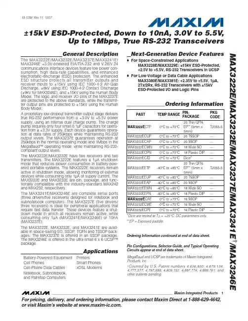
For pricing, delivery, and ordering information, please contact Maxim Direct at 1-888-629-4642,or visit Maxim's website at .General DescriptionThe MAX3222E/MAX3232E/MAX3237E/MAX3241E/MAX3246E +3.0V-powered EIA/TIA-232 and V.28/V.24communications interface devices feature low power con-sumption, high data-rate capabilities, and enhanced electrostatic-discharge (ESD) protection. The enhanced ESD structure protects all transmitter outputs and receiver inputs to ±15kV using IEC 1000-4-2 Air-G ap Discharge, ±8kV using IEC 1000-4-2 Contact Discharge (±9kV for MAX3246E), and ±15kV using the Human Body Model. The logic and receiver I/O pins of the MAX3237E are protected to the above standards, while the transmit-ter output pins are protected to ±15kV using the Human Body Model.A proprietary low-dropout transmitter output stage delivers true RS-232 performance from a +3.0V to +5.5V power supply, using an internal dual charge pump. The charge pump requires only four small 0.1µF capacitors for opera-tion from a +3.3V supply. Each device guarantees opera-tion at data rates of 250kbps while maintaining RS-232output levels. The MAX3237E guarantees operation at 250kbps in the normal operating mode and 1Mbps in the MegaBaud™ operating mode, while maintaining RS-232-compliant output levels.The MAX3222E/MAX3232E have two receivers and two transmitters. The MAX3222E features a 1µA shutdown mode that reduces power consumption in battery-pow-ered portable systems. The MAX3222E receivers remain active in shutdown mode, allowing monitoring of external devices while consuming only 1µA of supply current. The MAX3222E and MAX3232E are pin, package, and func-tionally compatible with the industry-standard MAX242and MAX232, respectively.The MAX3241E/MAX3246E are complete serial ports (three drivers/five receivers) designed for notebook and subnotebook computers. The MAX3237E (five drivers/three receivers) is ideal for peripheral applications that require fast data transfer. These devices feature a shut-down mode in which all receivers remain active, while consuming only 1µA (MAX3241E/MAX3246E) or 10nA (MAX3237E).The MAX3222E, MAX3232E, and MAX3241E are avail-able in space-saving SO, SSOP, TQFN and TSSOP pack-ages. The MAX3237E is offered in an SSOP package.The MAX3246E is offered in the ultra-small 6 x 6 UCSP™package.ApplicationsBattery-Powered Equipment PrintersCell PhonesSmart Phones Cell-Phone Data Cables xDSL ModemsNotebook, Subnotebook,and Palmtop ComputersNext-Generation Device Features♦For Space-Constrained ApplicationsMAX3228E/MAX3229E: ±15kV ESD-Protected, +2.5V to +5.5V, RS-232 Transceivers in UCSP ♦For Low-Voltage or Data Cable ApplicationsMAX3380E/MAX3381E: +2.35V to +5.5V, 1µA, 2Tx/2Rx, RS-232 Transceivers with ±15kV ESD-Protected I/O and Logic PinsMAX3222E/MAX3232E/MAX3237E/MAX3241E †/MAX3246E±15kV ESD-Protected, Down to 10nA, 3.0V to 5.5V ,Up to 1Mbps, True RS-232 Transceivers________________________________________________________________Maxim Integrated Products 119-1298; Rev 11; 10/07Ordering Information continued at end of data sheet.*Dice are tested at T A = +25°C, DC parameters only.**EP = Exposed paddle.Pin Configurations, Selector Guide, and Typical Operating Circuits appear at end of data sheet.MegaBaud and UCSP are trademarks of Maxim Integrated Products, Inc.†Covered by U.S. Patent numbers 4,636,930; 4,679,134;4,777,577; 4,797,899; 4,809,152; 4,897,774; 4,999,761; and other patents pending.M A X 3222E /M A X 3232E /M A X 3237E /M A X 3241E †/M A X 3246EUp to 1Mbps, True RS-232 TransceiversABSOLUTE MAXIMUM RATINGSELECTRICAL CHARACTERISTICS(V CC = +3V to +5.5V, C1–C4 = 0.1µF, T A = T MIN to T MAX , unless otherwise noted. Typical values are at T A = +25°C.) (Notes 3, 4)Stresses beyond those listed under “Absolute Maximum Ratings” may cause permanent damage to the device. These are stress ratings only, and functional operation of the device at these or any other conditions beyond those indicated in the operational sections of the specifications is not implied. Exposure to absolute maximum rating conditions for extended periods may affect device reliability.V CC to GND..............................................................-0.3V to +6V V+ to GND (Note 1)..................................................-0.3V to +7V V- to GND (Note 1)...................................................+0.3V to -7V V+ + |V-| (Note 1).................................................................+13V Input Voltages T_IN, EN , SHDN , MBAUD to GND ........................-0.3V to +6V R_IN to GND.....................................................................±25V Output Voltages T_OUT to GND...............................................................±13.2V R_OUT, R_OUTB (MAX3241E)................-0.3V to (V CC + 0.3V)Short-Circuit Duration, T_OUT to GND.......................Continuous Continuous Power Dissipation (T A = +70°C)16-Pin SSOP (derate 7.14mW/°C above +70°C)..........571mW 16-Pin TSSOP (derate 9.4mW/°C above +70°C).......754.7mW 16-Pin TQFN (derate 20.8mW/°C above +70°C).....1666.7mW 16-Pin Wide SO (derate 9.52mW/°C above +70°C).....762mW 18-Pin Wide SO (derate 9.52mW/°C above +70°C).....762mW 18-Pin PDIP (derate 11.11mW/°C above +70°C)..........889mW 20-Pin TQFN (derate 21.3mW/°C above +70°C)........1702mW 20-Pin TSSOP (derate 10.9mW/°C above +70°C)........879mW 20-Pin SSOP (derate 8.00mW/°C above +70°C)..........640mW 28-Pin SSOP (derate 9.52mW/°C above +70°C)..........762mW 28-Pin Wide SO (derate 12.50mW/°C above +70°C).............1W 28-Pin TSSOP (derate 12.8mW/°C above +70°C)......1026mW 32-Lead Thin QFN (derate 33.3mW/°C above +70°C)..2666mW 6 x 6 UCSP (derate 12.6mW/°C above +70°C).............1010mW Operating Temperature Ranges MAX32_ _EC_ _...................................................0°C to +70°C MAX32_ _EE_ _.................................................-40°C to +85°C Storage Temperature Range.............................-65°C to +150°C Lead Temperature (soldering, 10s).................................+300°C Bump Reflow Temperature (Note 2)Infrared, 15s..................................................................+200°C Vapor Phase, 20s..........................................................+215°C Note 1:V+ and V- can have maximum magnitudes of 7V, but their absolute difference cannot exceed 13V.Note 2:This device is constructed using a unique set of packaging techniques that impose a limit on the thermal profile the devicecan be exposed to during board-level solder attach and rework. This limit permits only the use of the solder profiles recom-mended in the industry-standard specification, JEDEC 020A, paragraph 7.6, Table 3 for IR/VPR and convection reflow.Preheating is required. Hand or wave soldering is not allowed.MAX3222E/MAX3232E/MAX3237E/MAX3241E †/MAX3246EUp to 1Mbps, True RS-232 Transceivers_______________________________________________________________________________________3M A X 3222E /M A X 3232E /M A X 3237E /M A X 3241E †/M A X 3246EUp to 1Mbps, True RS-232 Transceivers4_______________________________________________________________________________________TIMING CHARACTERISTICS—MAX3237E(V CC = +3V to +5.5V, C1–C4 = 0.1µF, T A = T MIN to T MAX , unless otherwise noted. Typical values are at T A = +25°C.) (Note 3)±10%. MAX3237E: C1–C4 = 0.1µF tested at +3.3V ±5%, C1–C4 = 0.22µF tested at +3.3V ±10%; C1 = 0.047µF, C2, C3, C4 =0.33µF tested at +5.0V ±10%. MAX3246E; C1-C4 = 0.22µF tested at +3.3V ±10%; C1 = 0.22µF, C2, C3, C4 = 0.54µF tested at 5.0V ±10%.Note 4:MAX3246E devices are production tested at +25°C. All limits are guaranteed by design over the operating temperature range.Note 5:The MAX3237E logic inputs have an active positive feedback resistor. The input current goes to zero when the inputs are atthe supply rails.Note 6:MAX3241EEUI is specified at T A = +25°C.Note 7:Transmitter skew is measured at the transmitter zero crosspoints.TIMING CHARACTERISTICS—MAX3222E/MAX3232E/MAX3241E/MAX3246EMAX3222E/MAX3232E/MAX3237E/MAX3241E †/MAX3246EUp to 1Mbps, True RS-232 Transceivers_______________________________________________________________________________________5-6-4-202460MAX3237ETRANSMITTER OUTPUT VOLTAGE vs. LOAD CAPACITANCE (MBAUD = GND)LOAD CAPACITANCE (pF)T R A N S M I T T E R O U T P U T V O L T A G E (V )10001500500200025003000531-1-3-5-6-2-42046-5-31-135010001500500200025003000LOAD CAPACITANCE (pF)T R A N S M I T T E R O U T P U T V O L T A G E (V )MAX3237ETRANSMITTER OUTPUT VOLTAGEvs. LOAD CAPACITANCE-7.5-5.0-2.502.55.07.5MAX3237ETRANSMITTER OUTPUT VOLTAGE vs. LOAD CAPACITANCE (MBAUD = V CC )LOAD CAPACITANCE (pF)T R A N S M I T T E R O U T P U T V O L T A G E (V )500100015002000__________________________________________Typical Operating Characteristics(V CC = +3.3V, 250kbps data rate, 0.1µF capacitors, all transmitters loaded with 3k Ωand C L , T A = +25°C, unless otherwise noted.)-6-5-4-3-2-10123456010002000300040005000MAX3241ETRANSMITTER OUTPUT VOLTAGEvs. LOAD CAPACITANCELOAD CAPACITANCE (pF)T R A N S M I T T E R O U T P U T V O L T A G E (V)302010405060020001000300040005000MAX3241EOPERATING SUPPLY CURRENT vs. LOAD CAPACITANCELOAD CAPACITANCE (pF)S U P P L Y C U R R E N T (m A )04286121014010002000300040005000MAX3241ESLEW RATE vs. LOAD CAPACITANCEM A X 3237E t o c 05LOAD CAPACITANCE (pF)S L E W R A T E (V /μs )-6-5-4-3-2-10123456010002000300040005000MAX3222E/MAX3232ETRANSMITTER OUTPUT VOLTAGEvs. LOAD CAPACITANCELOAD CAPACITANCE (pF)T R A N S M I T T E R O U T P UT V O L T A G E (V )624108141216010002000300040005000MAX3222E/MAX3232ESLEW RATE vs. LOAD CAPACITANCELOAD CAPACITANCE (pF)S L E W R A T E (V /μs)2520155103530404520001000300040005000MAX3222E/MAX3232E OPERATING SUPPLY CURRENT vs. LOAD CAPACITANCELOAD CAPACITANCE (pF)S U P P L Y C U R R E N T (m A )M A X 3222E /M A X 3232E /M A X 3237E /M A X 3241E †/M A X 3246EUp to 1Mbps, True RS-232 Transceivers6_______________________________________________________________________________________Typical Operating Characteristics (continued)(V CC = +3.3V, 250kbps data rate, 0.1µF capacitors, all transmitters loaded with 3k Ωand C L , T A = +25°C, unless otherwise noted.)20604080100MAX3237ETRANSMITTER SKEW vs. LOAD CAPACITANCE(MBAUD = V CC )LOAD CAPACITANCE (pF)100015005002000T R A N S M I T T E R S K E W (n s )-6-2-42046-3-51-1352.03.03.52.54.04.55.0SUPPLY VOLTAGE (V)T R A N S M I T T E R O U T P U T V O L T A G E (V )MAX3237ETRANSMITTER OUTPUT VOLTAGE vs. SUPPLY VOLTAGE (MBAUD = GND)10203040502.0MAX3237E SUPPLY CURRENT vs. SUPPLY VOLTAGE (MBAUD = GND)SUPPLY VOLTAGE (V)S U P P L Y C U R R E N T (m A )3.03.52.54.04.55.0MAX3246ETRANSMITTER OUTPUT VOLTAGEvs. LOAD CAPACITANCELOAD CAPACITANCE (pF)T R A N S M I T T E R O U T P U T V O L T A G E (V )4000300010002000-5-4-3-2-101234567-65000468101214160MAX3246ESLEW RATE vs. LOAD CAPACITANCELOAD CAPACITANCE (pF)S L EW R A T E (V /μs )200030001000400050001020304050600MAX3246EOPERATING SUPPLY CURRENT vs. LOAD CAPACITANCEM A X 3237E t o c 17LOAD CAPACITANCE (pF)S U P P L Y C U R R EN T (m A )1000200030004000500055453525155024681012MAX3237ESLEW RATE vs. LOAD CAPACITANCE(MBAUD = GND)LOAD CAPACITANCE (pF)S L E W R A T E (V /μs )10001500500200025003000010203050406070MAX3237ESLEW RATE vs. LOAD CAPACITANCE(MBAUD = V CC )LOAD CAPACITANCE (pF)S L E W R A T E (V /μs )5001000150020001020304050MAX3237ESUPPLY CURRENT vs. LOAD CAPACITANCE WHEN TRANSMITTING DATA (MBAUD = GND)LOAD CAPACITANCE (pF)S U P P L Y C U R R E N T (m A )10001500500200025003000MAX3222E/MAX3232E/MAX3237E/MAX3241E †/MAX3246EUp to 1Mbps, True RS-232 Transceivers_______________________________________________________________________________________7Pin DescriptionM A X 3222E /M A X 3232E /M A X 3237E /M A X 3241E †/M A X 3246EUp to 1Mbps, True RS-232 Transceivers8_______________________________________________________________________________________MAX3222E/MAX3232E/MAX3237E/MAX3241E †/MAX3246EUp to 1Mbps, True RS-232 Transceivers_______________________________________________________________________________________9Detailed DescriptionDual Charge-Pump Voltage ConverterThe MAX3222E/MAX3232E/MAX3237E/MAX3241E/MAX3246Es’ internal power supply consists of a regu-lated dual charge pump that provides output voltages of +5.5V (doubling charge pump) and -5.5V (inverting charge pump) over the +3.0V to +5.5V V CC range. The charge pump operates in discontinuous mode; if the output voltages are less than 5.5V, the charge pump is enabled, and if the output voltages exceed 5.5V, the charge pump is disabled. Each charge pump requires a flying capacitor (C1, C2) and a reservoir capacitor (C3, C4) to generate the V+ and V- supplies (Figure 1).RS-232 TransmittersThe transmitters are inverting level translators that con-vert TTL/CMOS-logic levels to ±5V EIA/TIA-232-compli-ant levels.The MAX3222E/MAX3232E/MAX3237E/MAX3241E/MAX3246E transmitters guarantee a 250kbps data rate with worst-case loads of 3k Ωin parallel with 1000pF,providing compatibility with PC-to-PC communication software (such as LapLink™). Transmitters can be par-alleled to drive multiple receivers or mice.The MAX3222E/MAX3237E/MAX3241E/MAX3246E transmitters are disabled and the outputs are forcedinto a high-impedance state when the device is in shut-down mode (SHDN = G ND). The MAX3222E/MAX3232E/MAX3237E/MAX3241E/MAX3246E permit the outputs to be driven up to ±12V in shutdown.The MAX3222E/MAX3232E/MAX3241E/MAX3246E transmitter inputs do not have pullup resistors. Connect unused inputs to GND or V CC . The MAX3237E’s trans-mitter inputs have a 400k Ωactive positive-feedback resistor, allowing unused inputs to be left unconnected.MAX3237E MegaBaud OperationFor higher-speed serial communications, the MAX3237E features MegaBaud operation. In MegaBaud operating mode (MBAUD = V CC ), the MAX3237E transmitters guarantee a 1Mbps data rate with worst-case loads of 3k Ωin parallel with 250pF for +3.0V < V CC < +4.5V. For +5V ±10% operation, the MAX3237E transmitters guarantee a 1Mbps data rate into worst-case loads of 3k Ωin parallel with 1000pF.RS-232 ReceiversThe receivers convert RS-232 signals to CMOS-logic output levels. The MAX3222E/MAX3237E/MAX3241E/MAX3246E receivers have inverting three-state outputs.Drive EN high to place the receiver(s) into a high-impedance state. Receivers can be either active or inactive in shutdown (Table 1).Figure 1. Slew-Rate Test CircuitsLapLink is a trademark of Traveling Software.M A X 3222E /M A X 3232E /M A X 3237E /M A X 3241E †/M A X 3246EUp to 1Mbps, True RS-232 Transceivers10______________________________________________________________________________________The complementary outputs on the MAX3237E/MAX3241E (R_OUTB) are always active, regardless of the state of EN or SHDN . This allows the device to be used for ring indicator applications without forward biasing other devices connected to the receiver outputs. This is ideal for systems where V CC drops to zero in shutdown to accommodate peripherals such as UARTs (Figure 2).MAX3222E/MAX3237E/MAX3241E/MAX3246E Shutdown ModeSupply current falls to less than 1µA in shutdown mode (SHDN = low). The MAX3237E’s supply current falls to10nA (typ) when all receiver inputs are in the invalid range (-0.3V < R_IN < +0.3). When shut down, the device’s charge pumps are shut off, V+ is pulled down to V CC , V- is pulled to ground, and the transmitter out-puts are disabled (high impedance). The time required to recover from shutdown is typically 100µs, as shown in Figure 3. Connect SHDN to V CC if shutdown mode is not used. SHDN has no effect on R_OUT or R_OUTB (MAX3237E/MAX3241E).±15kV ESD ProtectionAs with all Maxim devices, ESD-protection structures are incorporated to protect against electrostatic dis-charges encountered during handling and assembly.The driver outputs and receiver inputs of the MAX3222E/MAX3232E/MAX3237E/MAX3241E/MAX3246E have extra protection against static electricity. Maxim’s engineers have developed state-of-the-art structures to protect these pins against ESD of ±15kV without damage.The ESD structures withstand high ESD in all states:normal operation, shutdown, and powered down. After an ESD event, Maxim’s E versions keep working without latchup, whereas competing RS-232 products can latch and must be powered down to remove latchup.Furthermore, the MAX3237E logic I/O pins also have ±15kV ESD protection. Protecting the logic I/O pins to ±15kV makes the MAX3237E ideal for data cable applications.SHDN T2OUTT1OUT5V/div2V/divV CC = 3.3V C1–C4 = 0.1μFFigure 3. Transmitter Outputs Recovering from Shutdown or Powering UpMAX3222E/MAX3232E/MAX3237E/MAX3241E †/MAX3246EUp to 1Mbps, True RS-232 TransceiversESD protection can be tested in various ways; the transmitter outputs and receiver inputs for the MAX3222E/MAX3232E/MAX3241E/MAX3246E are characterized for protection to the following limits:•±15kV using the Human Body Model•±8kV using the Contact Discharge method specified in IEC 1000-4-2•±9kV (MAX3246E only) using the Contact Discharge method specified in IEC 1000-4-2•±15kV using the Air-G ap Discharge method speci-fied in IEC 1000-4-2Figure 4a. Human Body ESD Test ModelFigure 4b. Human Body Model Current WaveformFigure 5a. IEC 1000-4-2 ESD Test Model Figure 5b. IEC 1000-4-2 ESD Generator Current WaveformM A X 3222E /M A X 3232E /M A X 3237E /M A X 3241E †/M A X 3246EUp to 1Mbps, True RS-232 Transceiverscharacterized for protection to ±15kV per the Human Body Model.ESD Test ConditionsESD performance depends on a variety of conditions.Contact Maxim for a reliability report that documents test setup, test methodology, and test results.Human Body ModelFigure 4a shows the Human Body Model, and Figure 4b shows the current waveform it generates when dis-charged into a low impedance. This model consists of a 100pF capacitor charged to the ESD voltage of interest,which is then discharged into the test device through a 1.5k Ωresistor.IEC 1000-4-2The IEC 1000-4-2 standard covers ESD testing and performance of finished equipment; it does not specifi-cally refer to integrated circuits. The MAX3222E/MAX3232E/MAX3237E/MAX3241E/MAX3246E help you design equipment that meets level 4 (the highest level)of IEC 1000-4-2, without the need for additional ESD-protection components.The major difference between tests done using the Human Body Model and IEC 1000-4-2 is higher peak current in IEC 1000-4-2, because series resistance is lower in the IEC 1000-4-2 model. Hence, the ESD with-stand voltage measured to IEC 1000-4-2 is generally lower than that measured using the Human Body Model. Figure 5a shows the IEC 1000-4-2 model, and Figure 5b shows the current waveform for the ±8kV IEC 1000-4-2 level 4 ESD Contact Discharge test. The Air-G ap Discharge test involves approaching the device with a charged probe. The Contact Discharge method connects the probe to the device before the probe is energized.Machine ModelThe Machine Model for ESD tests all pins using a 200pF storage capacitor and zero discharge resis-tance. Its objective is to emulate the stress caused by contact that occurs with handling and assembly during manufacturing. All pins require this protection during manufacturing, not just RS-232 inputs and outputs.Therefore, after PC board assembly, the Machine Model is less relevant to I/O ports.Table 2. Required Minimum Capacitor ValuesFigure 6a. MAX3241E Transmitter Output Voltage vs. Load Current Per TransmitterTable 3. Logic-Family Compatibility with Various Supply VoltagesMAX3222E/MAX3232E/MAX3237E/MAX3241E †/MAX3246EUp to 1Mbps, True RS-232 TransceiversApplications InformationCapacitor SelectionThe capacitor type used for C1–C4 is not critical for proper operation; polarized or nonpolarized capacitors can be used. The charge pump requires 0.1µF capaci-tors for 3.3V operation. For other supply voltages, see Table 2 for required capacitor values. Do not use val-ues smaller than those listed in Table 2. Increasing the capacitor values (e.g., by a factor of 2) reduces ripple on the transmitter outputs and slightly reduces power consumption. C2, C3, and C4 can be increased without changing C1’s value. However, do not increase C1without also increasing the values of C2, C3, C4,and C BYPASS to maintain the proper ratios (C1 to the other capacitors).When using the minimum required capacitor values,make sure the capacitor value does not degradeexcessively with temperature. If in doubt, use capaci-tors with a larger nominal value. The capacitor’s equiv-alent series resistance (ESR), which usually rises at low temperatures, influences the amount of ripple on V+and V-.Power-Supply DecouplingIn most circumstances, a 0.1µF V CC bypass capacitor is adequate. In applications sensitive to power-supply noise, use a capacitor of the same value as charge-pump capacitor C1. Connect bypass capacitors as close to the IC as possible.Operation Down to 2.7VTransmitter outputs meet EIA/TIA-562 levels of ±3.7V with supply voltages as low as 2.7V.Figure 6b. Mouse Driver Test CircuitM A X 3222E /M A X 3232E /M A X 3237E /M A X 3241E †/M A X 3246EUp to 1Mbps, True RS-232 TransceiversFigure 7. Loopback Test CircuitT1IN T1OUTR1OUT5V/div5V/div5V/divV CC = 3.3V C1–C4 = 0.1μFFigure 8. MAX3241E Loopback Test Result at 120kbps T1INT1OUTR1OUT5V/div5V/div5V/divV CC = 3.3V, C1–C4 = 0.1μFFigure 9. MAX3241E Loopback Test Result at 250kbps+5V 0+5V 0-5V +5VT_INT_OUT5k Ω + 250pFR_OUTV CC = 3.3V C1–C4 = 0.1μFFigure 10. MAX3237E Loopback Test Result at 1000kbps (MBAUD = V CC )Transmitter Outputs Recoveringfrom ShutdownFigure 3 shows two transmitter outputs recovering from shutdown mode. As they become active, the two trans-mitter outputs are shown going to opposite RS-232 levels (one transmitter input is high; the other is low). Each transmitter is loaded with 3k Ωin parallel with 2500pF.The transmitter outputs display no ringing or undesir-able transients as they come out of shutdown. Note thatthe transmitters are enabled only when the magnitude of V- exceeds approximately -3.0V.Mouse DrivabilityThe MAX3241E is designed to power serial mice while operating from low-voltage power supplies. It has been tested with leading mouse brands from manu-facturers such as Microsoft and Logitech. The MAX3241E successfully drove all serial mice tested and met their current and voltage requirements.MAX3222E/MAX3232E/MAX3237E/MAX3241E †/MAX3246EUp to 1Mbps, True RS-232 TransceiversFigure 6a shows the transmitter output voltages under increasing load current at +3.0V. Figure 6b shows a typical mouse connection using the MAX3241E.High Data RatesThe MAX3222E/MAX3232E/MAX3237E/MAX3241E/MAX3246E maintain the RS-232 ±5V minimum transmit-ter output voltage even at high data rates. Figure 7shows a transmitter loopback test circuit. Figure 8shows a loopback test result at 120kbps, and Figure 9shows the same test at 250kbps. For Figure 8, all trans-mitters were driven simultaneously at 120kbps into RS-232 loads in parallel with 1000pF. For Figure 9, a single transmitter was driven at 250kbps, and all transmitters were loaded with an RS-232 receiver in parallel with 1000pF.The MAX3237E maintains the RS-232 ±5.0V minimum transmitter output voltage at data rates up to 1Mbps.Figure 10 shows a loopback test result at 1Mbps with MBAUD = V CC . For Figure 10, all transmitters were loaded with an RS-232 receiver in parallel with 250pF.Interconnection with 3V and 5V LogicThe MAX3222E/MAX3232E/MAX3237E/MAX3241E/MAX3246E can directly interface with various 5V logic families, including ACT and HCT CMOS. See Table 3for more information on possible combinations of inter-connections.UCSP ReliabilityThe UCSP represents a unique packaging form factor that may not perform equally to a packaged product through traditional mechanical reliability tests. UCSP reliability is integrally linked to the user’s assembly methods, circuit board material, and usage environ-ment. The user should closely review these areas when considering use of a UCSP package. Performance through Operating Life Test and Moisture Resistance remains uncompromised as the wafer-fabrication process primarily determines it.Mechanical stress performance is a greater considera-tion for a UCSP package. UCSPs are attached through direct solder contact to the user’s PC board, foregoing the inherent stress relief of a packaged product lead frame. Solder joint contact integrity must be consid-ered. Table 4 shows the testing done to characterize the UCSP reliability performance. In conclusion, the UCSP is capable of performing reliably through envi-ronmental stresses as indicated by the results in the table. Additional usage data and recommendations are detailed in the UCSP application note, which can be found on Maxim’s website at .Table 4. Reliability Test DataM A X 3222E /M A X 3232E /M A X 3237E /M A X 3241E †/M A X 3246EUp to 1Mbps, True RS-232 Transceivers__________________________________________________________Pin ConfigurationsMAX3222E/MAX3232E/MAX3237E/MAX3241E †/MAX3246EUp to 1Mbps, True RS-232 TransceiversPin Configurations (continued)M A X 3222E /M A X 3232E /M A X 3237E /M A X 3241E †/M A X 3246EUp to 1Mbps, True RS-232 Transceivers__________________________________________________Typical Operating CircuitsMAX3222E/MAX3232E/MAX3237E/MAX3241E †/MAX3246EUp to 1Mbps, True RS-232 Transceivers_____________________________________Typical Operating Circuits (continued)M A X 3222E /M A X 3232E /M A X 3237E /M A X 3241E †/M A X 3246EUp to 1Mbps, True RS-232 Transceivers_____________________________________Typical Operating Circuits (continued)MAX3222E/MAX3232E/MAX3237E/MAX3241E †/MAX3246EUp to 1Mbps, True RS-232 Transceivers______________________________________________________________________________________21Selector Guide___________________Chip InformationTRANSISTOR COUNT:MAX3222E/MAX3232E: 1129MAX3237E: 2110MAX3241E: 1335MAX3246E: 842PROCESS: BICMOSOrdering Information (continued)†Requires solder temperature profile described in the AbsoluteMaximum Ratings section. UCSP Reliability is integrally linked to the user’s assembly methods, circuit board material, and environment. Refer to the UCSP Reliability Notice in the UCSP Reliability section of this datasheet for more information.**EP = Exposed paddle.。
专芯发展•用芯服务•创芯未来产品特点●300µA 供电电流●确保最大120Kbps 数据传输率●确保最小3V/µs 压摆率●增强的ESD 规范:•IEC61000-4-2标准中±15kV 空气放电标准•IEC61000-4-2标准中±8kV 接触放电标准●可使用SOP-16和TSSOP-16封装产品应用●电池供电设备●掌上设备●周边设备●数据通信设备产品概述CBM3232是一种基于EIA/TIA-232标准和V.28/V.24标准的通讯接口,其供电电压为3.3V、具有低功耗需求,高数据传输率能力。
CBM3232有两个接收器和一个驱动器。
该设备可以确保以RS-232标准输出电平水平的情况下以120Kbps 数据传输率运行。
典型应用包括笔记本计算机、轻型便携掌上电脑、电池供电的设备、手持式设备、电子周边设备和打印机。
专芯发展•用芯服务•创芯未来目录产品特点..........................................................................................................................................1产品应用..........................................................................................................................................1产品概述..........................................................................................................................................1目录..................................................................................................................................................2引脚配置..........................................................................................................................................3引脚描述..........................................................................................................................................3绝对最大额定参数..........................................................................................................................4电气特性..........................................................................................................................................5逻辑输入电气特性..........................................................................................................................5发送电气特性..................................................................................................................................5应用电路..........................................................................................................................................7电容值(µF).....................................................................................................................................7典型运行特性..................................................................................................................................8静电保护..........................................................................................................................................9封装尺寸及结构............................................................................................................................12SOP-16......................................................................................................................................12TSSOP-16..................................................................................................................................13包装/订购信息.. (14)引脚配置引脚描述绝对最大额定值符号参数值单位V CC供电电压-0.3至6V V+复合终端电压(VCC-0.3)至7VV-反向终端电压0.3至-7VV++|V-|13V T IN发送器输入电压范围-0.3至6VR IN接收器输入电压范围±25V T OUT发送器输出电压范围±13.2V R OUT接收器输出电压范围-0.3to(VCC+0.3)VT a工作温度-40至85℃Ts储存温度-65至150℃t SHORT发送器输出短路接地时间持续*超出上述绝对最大额定值可能会导致器件永久性损坏。
Part Number Emitting Color Emitting MaterialLens-colorWavelength CIE127-2007*nm λPViewing Angle 2θ 1/2Luminous Intensity CIE127-2007* (I F =20mA) mcd *Luminous intensity value and wavelength are in accordance with CIE127-2007 standards.A Relative Humidity between 40% and 60% is recommended inESD-protected work areas to reduce static build up during assembly process (Reference JEDEC/JESD625-A and JEDEC/J-STD-033)Features● Ideal for indication light on hand held products ● Long life and robust package ● Standard Package: 2000pcs/ Reel ● MSL (Moisture Sensitivity Level): 3 ● Halogen-free ● RoHS compliantATTENTIONOBSERVE PRECAUTIONSFOR HANDLING ELECTROSTATIC DISCHARGE SENSITIVE DEVICESLED is recommended for reflow soldering and soldering profile is shown below.Forward Current Derating CurveThe device has a single mounting surface. The device must be mounted according to the specifications.Reel Dimension (Units : mm)Recommended Soldering Pattern (Units : mm; Tolerance: ± 0.1)Tape Specification (Units : mm)Remarks:If special sorting is required (e.g. binning based on forward voltage, Luminous intensity / luminous flux, or wavelength), the typical accuracy of the sorting process is as follows: 1. Wavelength: +/-1nm2. Luminous intensity / luminous flux: +/-15%3. Forward Voltage: +/-0.1VNote: Accuracy may depend on the sorting parameters.TERMS OF USE1. Data presented in this document reflect statistical figures and should be treated as technical reference only.2. Contents within this document are subject to improvement and enhancement changes without notice.3. The product(s) in this document are designed to be operated within the electrical and environmental specifications indicated on the datasheet. User accepts full risk and responsibility when operating the product(s) beyond their intended specifications.4. The product(s) described in this document are intended for electronic applications in which a person’s life is not reliant upon the LED. Please consult with a SunLED representative for special applications where the LED may have a direct impact on a person’s life.5. The contents within this document may not be altered without prior consent by SunLED.6. Additional technical notes are available at https:///TechnicalNotes.aspPACKING & LABEL SPECIFICATIONS。
sp3232中文资料_数据手册_参数SP3222E/SP3232ETrue +3.0V to +5.5V RS-232 TransceiversThe SP3222E/SP3232E series is an RS-232 transceiver solution intended for portable or hand-held applications such as notebook or palmtop computers. The SP3222E/SP3232E series has a high-efficiency, charge-pump power supply that requires only 0.1μF capaci -tors in 3.3V operation. This charge pump allows the SP3222E/SP3232E series to deliver true RS-232 performance from a single power supply ranging from +3.0V to +5.5V. The SP3222E/SP3232E are 2-driver/2-receiver devices. This series is ideal for portable or hand-held applications such as notebook or palmtop computers. The ESD tolerance of the SP3222E/SP3232E devices are over +/-15kV for both Human Body Model and IEC61000-4-2 Air discharge test methods. The SP3222E device has a low-power shutdown mode where thedevices' driver outputs and charge pumps are disabled. During shutdown, the supply current fal ls to less than 1μA.FEATURES■ Meets true EIA/TIA-232-F Standards from a +3.0V to +5.5V power supply ■ Minimum 120kbps Data Rate Under Full Load ■ 1μA Low Power Shutdown with Receivers active (SP3222E )■ Interoperable with RS-232 down to a +2.7V power source ■ Enhanced ESD Specifications: +15kV Human Body Model +15kV IEC61000-4-2 Air Discharge +8kV IEC61000-4-2 Contact DischargeDESCRIPTIONSELECTION TABLENow Available in Lead Free Packaging V-C1+V+C1-C2+C2-EN R2IN T2OUT nSOICMODELPower SuppliesRS-232 Drivers RS-232 Receivers External Components Shutdown TTL 3-State # of Pins SP3222E +3.0V to +5.5V 22 4 Capacitors Yes Yes 18, 20SP3232E +3.0V to +5.5V224 CapacitorsNoNo16Note: See page 6 for other pinoutsNOTE 1: V+ and V- can have maximum magnitudes of 7V, but their absolute difference cannot exceed 13V.These are stress ratings only and functional operation of the device at these ratings or any other above those indicated in theoperation sections of the specifications below is not implied. Exposure to absolute maximum rating conditions for extended periods of time may affect reliability and cause permanent damage to the device.V CC .......................................................-0.3V to +6.0V V+ (NOTE 1).......................................-0.3V to +7.0V V- (NOTE 1)........................................+0.3V to -7.0V V+ + |V-| (NOTE 1)...........................................+13V I CC (DC V CC or GND current).........................+100mAInput VoltagesTxIN, EN, SHDN...........................-0.3V to Vcc + 0.3V RxIN...................................................................+15V Output Voltages TxOUT.............................................................+13.2VRxOUT, .......................................-0.3V to (V CC +0.3V)Short-Circuit DurationTxOUT....................................................Continuous Storage Temperature......................-65°C to +150°CUnless otherwise noted, the following specifications apply for V CC = +3.0V to +5.5V with T AMB = T MIN to T MAX ,Power Dissipation per package20-pin SSOP (derate 9.25mW/o C above +70o C)..............750mW 18-pin SOIC (derate 15.7mW/o C above +70o C)..............1260mW 20-pin TSSOP (derate 11.1mW/o C above +70o C).............890mW 16-pin SSOP (derate 9.69mW/o C above +70o C)...............775mW 16-pin PDIP (derate 14.3mW/o C above +70o C)...............1150mW 16-pin Wide SOIC (derate 11.2mW/o C above +70o C)........900mW 16-pin TSSOP (derate 10.5mW/o C above +70o C)..............850mW 16-pin nSOIC (derate 13.57mW/o C above +70o C)...........1086mWELECTRICAL CHARACTERISTICSPARAMETERMIN.TYP .MAX.UNITSCONDITIONSDC CHARACTERISTICS Supply Current0.3 1.0mA no load, V CC = 3.3V,T AMB = 25o C, TxIN = GND or V CC Shutdown Supply Current1.010μASHDN = GND, VCC = 3.3V,T AMB = 25o C, TxIN = Vcc or GND LOGIC INPUTS AND RECEIVER OUTPUTS Input Logic Threshold LOW 0.8V TxIN, EN, SHDN, Note 2Input Logic Threshold HIGH 2.0Vcc V Vcc = 3.3V, Note 2Input Logic Threshold HIGH 2.4Vcc V Vcc = 5.0V, Note 2Inp ut Leakage Current +0.01+1.0μA TxIN, EN, SHDN,T AMB = +25o C, V IN = 0V to V CCOutput Leakage Current +0.05+10μA Receivers disabled, V OUT = 0V to V CC Output Voltage LOW 0.4V I OUT = 1.6mA Output Voltage HIGH V CC -0.6V CC -0.1VI OUT = -1.0mADRIVER OUTPUTS Output Voltage Swing+5.0+5.4VAll driver outputs loaded with 3k? to GND, T AMB = +25o C ABSOLUTE MAXIMUM RATINGSUnless otherwise noted, the following specifications apply for V CC = +3.0V to +5.5V with T AMB = T MIN to T MAX , Typical values apply at V CC = +3.3V or +5.0V and T AMB = 25°C.ELECTRICAL CHARACTERISTICSPARAMETERMIN.TYP .MAX.UNITSCONDITIONSDRIVER OUTPUTS (continued)Output Resistance300V CC = V+ = V- = 0V, T OUT =+2V Output Short-Circuit Current +35+60mA V OUT = 0VOutput Leakage Current +25μAV CC = 0V or 3.0V to 5.5V, V OUT = +12V, Drivers disabled RECEIVER INPUTS Input Voltage Range -15+15V Input Threshold LOW 0.6 1.2V Vcc = 3.3V Input Threshold LOW 0.81.5V Vcc = 5.0V Input Threshold HIGH 1.52.4V Vcc =3.3V Input Threshold HIGH 1.8 2.4V Vcc = 5.0VInput Hysteresis 0.3V Input Resistance357k?TIMING CHARACTERISTICS Maximum Data Rate 120235kbps R L = 3k?, C L = 1000pF, one driver switching Driver Propagation Delay, t PHL 1.0μs R L = 3k?, C L = 1000pF Driver Propagatio n Delay, t PLH 1.0μs R L = 3k?, C L = 1000pF Receiver Propagation Delay, t PHL0.3μs Receiver input to Receiver output, C L = 150pF Receiver Propagation Delay, t PLH 0.3μs Receiver input to Receiver output, C L = 150pFReceiver Output Enable Time 200ns Receiver Output Disable Time 200ns Driver Skew 100500ns | t PHL - t PLH |, T AMB = 25°C Receiver Skew2001000ns | t PHL - t PLH |Transition-Region Slew Rate30V/μsVcc = 3.3V, R L = 3k?, C L = 1000pF, T AMB = 25°C,measurements taken from -3.0V to +3.0V or +3.0V to -3.0V NOTE 2: Driver input hysteresis is typically 250mV.Unless otherwise noted, the following performance characteristics apply for V CC = +3.3V, 120kbps data rate, all drivers loaded with 3k?, 0.1μF charge pump capacitors, and T AMB = +25°C.Figure 2. Slew Rate vs Load Capacitance for the SP3222E and SP3232EFigure 1. Transmitter Output Voltage vs LoadCapacitance for the SP3222E and SP3232E Figure 3. Supply Current VS. Load Capacitance when Transmitting DataTYPICAL PERFORMANCE CHARACTERISTICSNAME FUNCTIONPIN NUMBERSP3222E SP3232E SOIC SSOPTSSOPEN Receiver Enable. Apply Logic LOW for normal operation.Apply logic HIGH to disable the receiver outputs (high-Z state)11-C1+Positive terminal of the voltage doubler charge-pump capacitor221V++5.5V output generated by the charge pump332 C1-Negative terminal of the voltage doubler charge-pump capacitor443 C2+Positive terminal of the inverting charge-pump capacitor554 C2-Negative terminal of the inverting charge-pump capacitor665 V--5.5V output generated by the charge pump776 T1OUT RS-232 driver output.151714T2OUT RS-232 driver output.887R1IN RS-232 receiver input141613R2IN RS-232 receiver input998R1OUT TTL/CMOS receiver output131512R2OUT TTL/CMOS receiver output10109T1IN TTL/CMOS driver input121311T2IN TTL/CMOS driver input111210 GND Ground161815VCC+3.0V to +5.5V supply voltage171916SHDN Shutdown Control Input. Drive HIGH for normal device operation.Drive LOW to shutdown the drivers (high-Z output) and the on-board power supply1820-N.C.No Connect-11, 14-PIN FUNCTIONTable 1. Device Pin DescriptionPINOUTFigure 5. Pinout Configuration for the SP3232EThe SP3222E/SP3232E transceivers meet the EIA/TIA-232 and ITU-T V.28/V.24 communication protocols and can be imple-mented in battery-powered, portable, or hand-held applications such as notebook or palmtop computers. The SP3222E/SP3232E devices feature Exar's proprietary on-board charge pumpcircuitry tha t generates ±5.5V for RS-232 voltage levels from a single +3.0V to +5.5V power supply. This series is ideal for +3.3V-only systems, mixed +3.3V to +5.5V systems, or +5.0V-only systems that require true RS-232 performance. The SP3222E/SP3232E devices can operate at a typical data rate of 235kbps when fully loaded.The SP3222E and SP3232E are 2-driver/2- receiver devices ideal for portable or hand-held applications. The SP3222E features a 1μA shutdown mode that reduces power consumption and extends battery life in por-table systems. Its receivers remain active in shutdown mode, allowing external devices such as modems to be monitored using only 1μA supply current.THEORY OF OPERATIONThe SP3222E/SP3232E series is made up of three basic circuit blocks:1. Drivers2. Receivers3. The Exar proprietary charge pumpDriversThe drivers are inverting level transmitters that convert TTL or CMOS logic levels to +5.0V EIA/TIA-232 levels with an inverted sense relative to the input logic levels. Typically, the RS-232 output voltage swing is +5.4V with no load and +5V minimum fully loaded. The driver outputs are protected against infinite short-circuits to ground with-out degradation in reliability. Driver outputs will meet EIA/TIA-562 levels of +/-3.7V with supply voltages as low as 2.7V.The drivers can guarantee a data rate of 120kbps fully loaded with 3k? in parallelwith 1000pF, ensuring compatability withPC-to-PC communication software.The slew rate of the driver is internally limitedto a maximum of 30V/μs in order t o meet theEIA standards (EIA RS-232D 2.1.7, Para-graph 5). The transition of the loaded outputfrom HIGH to LOW also meet the monotonic-ity requirements of the standard.Figure 8 shows a loopback test circuitused to test the RS-232 Drivers. Figure9 shows the test results of the loopbackcircuit with all drivers active at 120kbpswith RS-232 loads in parallel with a1000pF capacitor. Figure 10 shows thetest results where one driver was activeat 235kbps and all drivers loaded with anRS-232 receiver in parallel with 1000pFcapacitors. A solid RS-232 data transmis-sion rate of 120kbps provides compatibilitywith many designs in personal computerperipherals and LAN applications.The SP3222E driver's output stages areturned off (tri-state) when the device is inshutdown mode. When the power is off, theSP3222E device permits the outputs to be driven up to +/-12V. The driver's inputs donot have pull-up resistors. Designers shouldconnect unused inputs to Vcc or GND.In the shutdown mode, the supply currentfalls to less than 1μA, where SHDN = LOW.When the SP3222E device is shut down,the device's driver outputs are disabled (tri-stated) and the charge pumps are turned offwith V+ pulled down to Vcc and V- pulled toGND. The time required to exit shutdown istypically 100μs. Connect SHDN to Vcc if theshutdown mode is not used.ReceiversThe Receivers convert EIA/TIA-232 levels to TTL or CMOS logic output levels. The SP3222E receivers have an inverting tri-state output. These receiver outputs (RxOUT) are tri-stated when the enable control EN = HIGH. In the shutdown mode, the receivers can be active or inactive. EN has no effect on TxOUT. The truth table logic of the SP3222E driver and receiver outputs can be found in Table 2.Since receiver input is usually from a trans -mission line where long cable lengths and system interference can degrade the signal, the inputs have a typical hysteresis margin of 300mV. This ensures that the receiver is virtually immune to noisy transmission lines. Should an input be left unconnected, an internal 5k? pulldown resistor to ground will commit the output of the receiver to a HIGH state.Table 2. SP3222E Truth Table Logic for Shutdown and Enable ControlCircuitCharge PumpThe charge pump is an Exar-patended design (U.S. 5,306,954) and uses a unique approach compared to older less-efficient designs. The charge pump still requires four external capacitors, but uses a four-phase voltage shifting technique to attain sym -metrical 5.5V power supplies. The internal power supply consists of a regulated dual charge pump that provides output voltages of +/-5.5V regardless of the input voltage (Vcc) over the +3.0V to +5.5V range.Figure 9. Loopback Test results at 120kbpsSHDN EN TxOUT RxOUT 00Tri-state Active 01Tri-state Tri-state 10Active Active 11ActiveTri-stateIn most circumstances, decoupling the power supply can be achieved adequately using a 0.1μF bypass capacitor at C5 (refer to figures 6 and 7). In applications that are sensitive to power-supply noise, decouple Vcc to ground with a capacitor of the same value as charge-pump capacitor C1. Physi -cally connect bypass capcitors as close to the IC as possible.The charge pump operates in a discontinu-ous mode using an internal oscillator. If the output voltages are less than a magnitude of 5.5V, the charge pump is enabled. If the output voltages exceed a magnitude of 5.5V, the charge pump is disabled. This oscillator controls the four phases of the voltage shift-ing. A description of each phase follows.Phase 1 — V SS charge storage — During this phase of the clock cycle, the positive side of capaci -tors C 1 and C 2 are initially charged to V CC . C l +is then switched to GND and the charge in C 1– is transferredto C 2–. Since C 2+ is con-nected to V CC , the voltage potential across capacitor C 2 is now 2 times V CC .Phase 2—V SS transfer —Phase two of the clock connects the negative terminal of C 2 to the V SS storage capacitor and the positive terminal of C 2 to GND. This transfers a negative gener-ated voltage to C 3. This generated voltage is regulated to a minimum voltage of -5.5V. Simultaneous with the transfer of the volt-age to C 3, the positive side of capacitor C 1 is switched to V CC and the negative side is connected to GND.Phase 3— V DD charge storage — The third phase of the clock is identical to the first phase —the charge transferred in C 1 produces –V CC in the negative terminal of C 1, which is applied to the negative side of capacitor C 2. Since C 2+ is at V CC , the voltage potential across C 2 is 2 times V CC .Phase 4— V DD transfer — The fourth phase of the clock connects the negative terminal of C 2 to GND, and transfers this positive generated voltage across C 2 to C 4, the V DD storage capacitor. This voltage is regulated to +5.5V. At this voltage, the in -ternal oscillator is disabled. Simultaneous with the transfer of the voltage to C 4, the positive side of capacitor C 1 is switched to V CC and the negative side is con-nected to GND, allowing the charge pump cycle to begin again. The charge pump cycle will continue as long as the operational conditions for the internal oscillator are present.Since both V + and V – are separately gener -ated from V CC , in a no–load condition V + and V – will be symmetrical. Older charge pump approaches that generate V – from V + will show adecrease in the magnitude of V – compared to V + due to the inherent inefficiencies in the design.The clock rate for the charge pump typically operates at greater than 250kHz. The exter -nal capacitors can be as low as 0.1μF with a 16V breakdown voltage rating.Figure 13. Charge Pump WaveformsESD TOLERANCEThe SP3222E/SP3232E series incorpo-rates ruggedized ESDcells on all driver output and receiver input pins. The ESD structure is improved over our previous family for more rugged applications and environments sensitive to electro-static discharges and associated transients. The improved ESD tolerance is at least +15kV without damage nor latch-up.There are different methods of ESD testing applied:a) MIL-STD-883, Method 3015.7b) IEC61000-4-2 Air-Dischargec) IEC61000-4-2 Direct ContactThe Human Body Model has been the generally accepted ESD testing method for semi-conductors. This method is also specified in MIL-STD-883, Method 3015.7 for ESD testing. The premise of this ESD test is to simulate the human body’s potential to store electro-static energy and discharge it to an integrated circuit. The simulation is performed by using a test model as shown in Figure 16. This method will test the IC’s capability to withstand an ESD transient during normal handling such as in manu-facturing areas where the ICs tend to be handled frequently.The IEC-61000-4-2, formerly IEC801-2, is generally used for testing ESD on equipment and systems. For system manufacturers, they must guarantee a certain amount of ESD protection since the system itself is exposed to the outside environment and human pres-ence. The premise with IEC61000-4-2 is that the system is required to withstand an amount of static electricity when ESD is applied to points and surfaces of the equipment that are accessible to personnel during normal usage. The transceiver IC receives most of the ESD current when the ESD source is applied to the connector pins. The test circuit for IEC61000-4-2 is shown on Figure 17. There are two methodswithin IEC61000-4-2, the Air Discharge method and the Contact Discharge method.With the Air Discharge Method, an ESD voltage is applied to the equipment under test (EUT) through air. This simulates an electrically charged person ready to connect a cable onto the rear of the system only to find an unpleasant zap just before the person touches the back panel. The high energy potential on the person discharges through an arcing path to the rear panel of the system before he or she even touches the system. This energy, whether discharged directly or through air, is predominantly a function of the discharge current rather than the discharge voltage. Variables with an air discharge such as approach speed of the object carrying the ESD potential to the system and humidity will tend to change the discharge current. For example, the rise time of the discharge current varies with the approach speed.The Contact Discharge Method applies the ESD current directly to the EUT. This method was devised to reduce the unpredictability of the ESD arc. The discharge current rise time is constant since the energy is directly transferred without the air-gap arc. In situ-ations such as hand held systems, the ESD charge can be directly discharged to theFigure 16. ESD Test Circuit for Human Body ModelDEVICE PIN HUMAN BODY IEC61000-4-2 TESTED MODEL AirDischarge Direct Contact LevelDriver Outputs +15kV +15kV +8kV4Receiver Inputs +15kV+15kV+8kV4equipment from a person already holding the equipment. The current is transferred on to the keypad or the serial port of the equipment directly and then travels through the PCB and finally to the IC.The circuit models in Figures 16 and 17 rep-resent the typical ESD testing circuit used for all three methods. The C S is initially charged with the DC power supply when the first switch (SW1) is on. Now that the capacitor is charged, the second switch (SW2) is on while SW1 switches off. The voltage stored in the capacitor is then applied through R S , the current limiting resistor, onto the device under test (DUT). In ESD tests, the SW2 switch is pulsed so that the device under test receives a duration of voltage. For the Human Body Model, the current limiting resistor (R S ) and the source capacitor (C S ) are 1.5k? an 100pF, respectively. For IEC-61000-4-2, the current limiting resistor (R S ) and the source capacitor (C S ) are 330? an 150pF, respectively .Figure 18. ESD Test Waveform for IEC61000-4-2Figure 17. ESD Test Circuit for IEC61000-4-2Table 3. Transceiver ESD Tolerance Levelst = 0nst = 30ns0A15A30AI →t →The higher C S value and lower R S value in the IEC61000-4-2 model are more stringent than the Human Body Model. The larger storage capacitor injects a higher voltage to the test point when SW2 is switched on. The lower current limiting resistor increases the current charge onto the test point.PACKAGE: 20 PIN SSOPPACKAGE: 16 PIN SSOPPACKAGE: 16 PIN PDIPPACKAGE: 16 PIN WSOIC。
2 Port USB to RS232 RS422 RS485 Serial Adapter with COM RetentionProduct ID: ICUSB2324852The ICUSB2324852 2 Port USB to RS232 RS422 RS485 Serial Adapter with COM Retention lets you connect every type of serial device to your USB-enabled computer, whether it be for RS232, RS422, or RS485 communication. The adapter features a 9-pin (DB9) male and a 5-pin terminal block serial connector as well as dip-switch controls for easy port configuration with minimal software requirements. The adapter also supports using 2 ports simultaneously, including with mixed protocols; for example RS-232 on port 1, and RS-485 on port 2, or a number of other combinations.For a convenient, and clean installation in office or industrial settings, the RS232/RS422/RS485 USB Adapter is wall-mountable and fully powered via the host USB connection, providing power to the attached serial device without requiring an external power adapter.Backed by a 2-year warranty and free lifetime technical support.Certifications, Reports and Compatibility Applications•Adapting and expanding POS systems•Great for Industrial programmers looking to test new code with serial devices•Connect serial RS232, RS422, or RS485 devices to notebooks ortablet PC’s through the USB port•Perfect for controlling, monitoring, and diagnosing manufacturing machines (CNC, Process Control Equipment, Bar Code Scanners,Serial Printers)•Security device control (key panels, cameras, card readers)Features•Backwards compatible with USB 1.1•USB-powered; No additional external power adapter required •Both ports can function simultaneously with mixed or matchedcommunication protocols•Includes a bracket for wall mounting the USB to Serial adapter •Features rugged screw-lock USB port to ensure cords are not accidentally disconnected•Ability to rename devices for easy recognition•COM Port assignments maintained after reboot•Port 1 (DB9) configurable for RS232, RS422, or RS485; Port 2 (Terminal Block) configurable for RS422 or RS485•Multiple interface modes, including: 4 wire RS422(TxD+/-, RxD+/-), and 2 wire RS485 (DATA+, DATA-)•Supports RS-485 Auto Transceiver Turn Around by Unique Featured ATTA Hardware•External power adapter can be used (not required) if your device needs extra power beyond what the USB host can provide •Transmission Echo for RS485 collision detection•USB to 2 Port Straight-Through RS232/422/485 Serial AdapterWarranty 2 YearsHardware Bus Type USB 2.0Chipset ID FTDI - FT2232HInterface SerialPort Style External HubPorts2Performance Data Bits7, 8FIFO128 BytesFlow Control Xon/Xoff, Hardware, and NoneMax Baud Rate921.6 KbpsParity Odd, Even, Mark, Space, and NoneSerial Protocol RS-232/422/485Stop Bits1, 2Connector(s)Connector Type(s) 1 - USB Type-A (4 pin) USB 2.0 MaleExternal Ports 1 - DB-9 (9 pin, D-Sub) Male1 - Terminal Block (5 Wire)Software OS Compatibility Windows® CE (4.2, 5.0, 6.0), XP Embedded, 98SE, 2000,XP, Vista, 7, 8, 8.1, 10Windows Server® 2003, 2008 R2, 2012, 2012 R2, 2016,2019Mac OS X® 10.6 to 10.15Linux 2.4.x to 4.4.x LTS Versions onlyIndicators LED Indicators 1 - Red - Power LEDPower Center Tip Polarity PositiveOutput Current0.385AOutput Voltage 5 DCPlug Type BPower Source Not Included (not required for standard applications) Environmental Humidity5~95% RHOperating Temperature0°C to 55°C (32°F to 131°F)Storage Temperature-20°C to 85°C (-4°F to 185°F)PhysicalColor GrayCharacteristicsEnclosure Type PlasticProduct Height0.9 in [2.3 cm]Product Length 3.2 in [82.3 mm]Product Width 1.7 in [44.2 mm]Weight of Product10.6 oz [300 g]PackagingPackage Height 1.6 in [40 mm]InformationPackage Length8.2 in [20.8 cm]Package Width 5.7 in [14.4 cm]Shipping (Package) Weight10.9 oz [310 g]What's in the Box Included in Package 1 - Wall mounting bracket1 - USB to RS232/RS422/485 Adapter1 - USB A to B Cable1 - Driver CD1 - Installation GuideProduct appearance and specifications are subject to change without notice.。