AUO_友达_液晶显示屏B140XW02_V0_01_PCB_电路图
- 格式:pdf
- 大小:136.37 KB
- 文档页数:8
( V ) Preliminary Specifications( ) Final SpecificationsModule 10.4 Inch Color TFT-LCD Model Name G104STN01.0Customer Date Checked &Approved by Approved by DateGrace Hung 2013/08/16 Prepared byJohnson Lin 2013/08/16 General Display Business Division / AU Optronics corporationContents1. Operating Precautions (4)2. General Description (5)2.1 Display Characteristics (5)2.2 Optical Characteristics (6)3. Functional Block Diagram (9)4. Absolute Maximum Ratings (10)4.1 Absolute Ratings of TFT LCD Module (10)4.2 Absolute Ratings of Environment (10)5. Electrical Characteristics (11)5.1 TFT LCD Module (11)5.2 Backlight Unit (13)6. Signal Characteristics (14)6.1 Pixel Format Image (14)6.2 Scanning Direction (14)6.3 TFT-LCD Interface Signal Description (15)6.4 The Input Data Format (16)6.5 TFT-LCD Interface Timing (17)6.6 Power ON/OFF Sequence (18)7. Connector & Pin Assignment (19)7.1 TFT-LCD Signal (CN1): LVDS Connector (19)7.2 LED Backlight Unit (CN2): Driver Connector (19)7.3 LED Backlight Unit (CN4): Light bar Connector (19)8. Reliability Test Criteria (20)9. Mechanical Characteristics (21)9.1 LCM Outline Dimension (Front View) (21)9.2 LCM Outline Dimension (Rear View) (22)10. Label and Packaging (23)10.1 Shipping Label (on the rear side of TFT-LCD display) (23)10.2 Carton Package (23)11 Safety (25)11.1 Sharp Edge Requirements (25)11.2 Materials (25)11.3 Capacitors (25)11.4 National Test Lab Requirement (25)Record of RevisionVersion and Date Page Old description New Description1. Operating Precautions1) Since front polarizer is easily damaged, please be cautious and not to scratch it.2) Be sure to turn off power supply when inserting or disconnecting from input connector.3) Wipe off water drop immediately. Long contact with water may cause discoloration orspots.4) When the panel surface is soiled, wipe it with absorbent cotton or soft cloth.5) Since the panel is made of glass, it may be broken or cracked if dropped or bumped onhard surface.6) To avoid ESD (Electro Static Discharde) damage, be sure to ground yourself before handlingTFT-LCD Module.7) Do not open nor modify the module assembly.8) Do not press the reflector sheet at the back of the module to any direction.9) In case if a module has to be put back into the packing container slot after it was takenout from the container, do not press the center of the LED light bar edge. Instead, press at the far ends of the LED light bar edge softly. Otherwise the TFT Module may be damaged.10) At the insertion or removal of the Signal Interface Connector, be sure not to rotate nortilt the Interface Connector of the TFT Module.11) TFT-LCD Module is not allowed to be twisted & bent even force is added on module in a veryshort time. Please design your display product well to avoid external force applying to module by end-user directly.12) Small amount of materials without flammability grade are used in the TFT-LCD module. TheTFT-LCD module should be supplied by power complied with requirements of Limited Power Source (IEC60950 or UL1950), or be applied exemption.13) Severe temperature condition may result in different luminance, response time and lampignition voltage.14) Continuous operating TFT-LCD display under low temperature environment may acceleratelamp exhaustion and reduce luminance dramatically.15) The data on this specification sheet is applicable when LCD module is placed in landscapeposition.16) Continuous displaying fixed pattern may induce image sticking. It’s recommended to usescreen saver or shuffle content periodically if fixed pattern is displayed on the screen.2. General DescriptionThis specification applies to the Color Active Matrix Liquid Crystal Display G104STN01.0composed of a TFT-LCD display, a driver and power supply circuit, and a LED backlight system. The screen format is intended to support SVGA (800(H) x 600(V)) screen and 16.2M (RGB 8-bits) or 262k colors (RGB 6-bits).LED driving board for backlight unit is included in G104STN01.0 and the LED unit is replaceable. All input signals are LVDS interface and compatible with G104SN02 V2.G104STN01.0 designed with wide viewing angle; wide temperature and long life LED backlight is well suited for industial applications. G104STN01.0 is a RoHS product.2.1 Display CharacteristicsThe following items are characteristics summary on the table under 25 ℃ condition: ItemsUnitSpecifications Screen Diagonal [inch] 10.4Active Area [mm] 211.2 (H) x 158.4 (V) Pixels H x V 800 x 3(RGB) x 600 Pixel Pitch [mm] 0.264 x 0.264 Pixel Arrangement R.G.B. Vertical Stripe Display ModeTN, Normally White Nominal Input Voltage VDD [Volt] 3.3 (typ.) Typical Power Consumption [Watt] 2.88WAll black pattern Weight [Grams] 365(Typ.)Physical Size [mm] 243.0(H) x 184.0(V) x 6.5(D)(Typ.) Electrical Interface 1 channel LVDS Surface Treatment Anti-glare, Hardness 3H Support Color16.2M / 262K colors Temperature Range OperatingStorage (Non-Operating) [o C] [o C]-20 to +80 -20 to +80 RoHS ComplianceRoHS Compliance2.2 Optical CharacteristicsThe optical characteristics are measured under stable conditions at 25 (Room Temperature):℃Item Unit Conditions Min. Typ. Max. RemarkWhite Luminance[cd/m2] I F = 50mA/1 LED Line (center point) 300 400 -1 Uniformity % 5 Points 65 75 -2,3 Contrast Ratio500 700 - 4[msec]Rising - 10 20 [msec] Falling- 5 15 Response Time[msec] Raising + Falling - 15 35 5 [degree] [degree] Horizontal (Right) CR = 10 (Left) 70 70 80 80 - - Viewing Angle[degree] [degree]Vertical (Upper) CR = 10 (Lower) 50 60 60 70 - - 6 Red x - TBD - Red y - TBD - Green x- TBD - Green y - TBD - Blue x - TBD - Blue y - TBD - White x 0.28 0.31 0.34 Color / ChromaticityCoordinates (CIE 1931)White y0.30 0.33 0.36 Color Gamut%50-Note 1: Measurement method Equipment Pattern Generator, Power Supply, Digital Voltmeter, Luminance meter (SR_3 or equivalent) Aperture1with 50cm viewing distance ∘Test Point CenterEnvironment < 1 luxModule Driving EquipmentNote 2: Definition of 5 points position (Display active area: 211.2mm (H) x 158.4mm (V))Note 3: The luminance uniformity of 5 points is defined by dividing the minimum luminance values by the maximum test point luminanceNote 4: Definition of contrast ratio (CR):Note 5: Definition of response time:The output signals of photo detector are measured when the input signals are changed from “White” to “Black” (falling time) and from “Black” to “White” (rising time), respectively. The response time interval isNote 6: Definition of viewing angleViewing angle is the measurement of contrast ratio 10, at the screen center, over a 180° horizontal and ≧180° vertical range (off-normal viewing angles). The 180° viewing angle range is broken down as below: 90° (θ) horizontal left and right, and 90° (Φ) vertical high (up) and low (down). The measurement direction is typically perpendicular to the display surface with the screen rotated to its center to develop the desiredMinimum Brightness of five pointsδW9 = Maximum Brightness of five points Contrast ratio (CR)=Brightness on the “White” stateBrightness on the “Black” statemeasurement viewing angle.3. Functional Block DiagramThe following diagram shows the functional block of the 10.4 inch color TFT/LCD module:4. Absolute Maximum Ratings4.1 Absolute Ratings of TFT LCD ModuleItem Symbol Min Max Unit Logic/LCD Drive Voltage Vin -0.3 +4.0 [Volt]4.2 Absolute Ratings of EnvironmentItem Symbol Min Max Unit Operating Temperature TOP -20 +80 [o C] Operation Humidity HOP 5 95 [%RH] Storage Temperature TST -20 +80 [o C] Storage Humidity HST 5 95 [%RH] Note: Maximum Wet-Bulb should be 39℃ and no condensation.5. Electrical Characteristics 5.1 TFT LCD Module5.1.1 Power SpecificationSymbol Parameter Min Typ Max Units RemarkVDD Logic/LCD Input Voltage 3.0 3.3 3.6 [Volt]I VDD LCD Input Current - 320 - [mA]VDD=3.3V at 60 HZ, all Black PatternP VDD LCD Power comsumption - - 1.5 [Watt] VDD=3.3V at 60 HZ, all Black Pattern I rush LCDLCD Inrush Current-1.06-[A] Note 1; VDD=3.3VBlack Pattern, Rising time=470usVDD rpAllowable Logic/LCDDrive Ripple Voltage- -100 [mV] p-pVDD=3.3V at 60 HZ, all Black PatternNote 1: Measurement condition:VDD rising time0V3.3V5.1.2 Signal Electrical CharacteristicsInput signals shall be low or Hi-Z state when VDD is off.Note: LVDS Signal Waveform.Symbol ItemMin. Typ.Max. Unit RemarkVTH Differential Input High Threshold - - 100 [mV] VCM=1.2V VTL Differential Input Low Threshold 100 - - [mV] VCM=1.2V |VID |Input Differential Voltage100 400 600 [mV] VICMDifferential Input Common Mode Voltage1.1251.251.375[V]VTH/VTL=+-100mV5.2 Backlight Unit5.2.1 Parameter guideline for LED backlightFollowing characteristics are measured under a stable condition using a inverter at 25℃. (Room Temperature): Symbol Parameter Min.Typ.Max.Unit RemarkVCC Input Voltage 10.8 12 12.6 [Volt]I VCC Input Current - 0.32 - [A] 100% PWM DutyP VCC Power Consumption - 2.88 - [Watt] 100% PWM DutyF PWM Dimming Frequency 200 - 20K [Hz]Swing Voltage 3 3.3 5.5 [Volt]Dimming duty cycle 5 - 100 %I F LED Forward Current-50 -[mA] Ta = 25o C- 27.2 - [Volt]I F = 50mA, Ta = -30o C V F LED Forward Voltage- 26.4 28.8 [Volt]I F = 50mA, Ta = 25o C- 25.6 - [Volt]I F = 50mA, Ta = 85o C P LED LED Power Consumption- 2.72 - [Watt]Operation Life 50,000 - - Hrs I F=50mA, Ta= 25o CNote 1: Ta means ambient temperature of TFT-LCD module.Note 2: VCC, I VCC, I rush LED, P VCC are defined for LED backlight.(100% duty of PWM dimming)Note 3: I F, V F are defined for one channel LED. There are two LED channel in back light unit.Note 4: If G104STN01.0 module is driven by high current or at high ambient temperature & humidity condition. The operating life will be reduced.Note 5: Operating life means brightness goes down to 50% initial brightness. Minimum operating life time is estimated data.6. Signal Characteristics6.1 Pixel Format ImageFollowing figure shows the relationship between input signal and LCD pixel format.1st2nd799th800th1stLine600thLin6.2 Scanning DirectionThe following figures show the image seen from the front view. The arrow indicates the direction of scan.Fig. 1 Normal scan (Pin4, DPS = Low or NC) Fig. 2 Reverse scan (Pin4, DPS = High)6.3 TFT-LCD Interface Signal DescriptionThe module using a LVDS receiver embaded in AUO’s ASIC. LVDS is a differential signal technology for LCD interface and a high-speed data transfer device.Input Signal Interface Pin No. SymbolDescription 1 VDD Power Supply, 3.3V (typical) 2 VDD Power Supply, 3.3V (typical) 3 GND Ground4 DPS Reverse Scan Function [H: Enable; L/NC: Disable]5 RxIN0-6 RxIN0+ LVDS receiver signal channel 0LVDS Differential Data Input (R0, R1, R2, R3, R4, R5, G0)7 GND Ground8 RxIN1- 9 RxIN1+ LVDS receiver signal channel 1LVDS Differential Data Input (G1, G2, G3, G4, G5, B0, B1) 10 GND Ground11 RxIN2- 12 RxIN2+ LVDS receiver signal channel 2LVDS Differential Data Input (B2, B3, B4, B5, DE)13 GNDGround14 RxCLKIN- 15 RxCLKIN+ LVDS receiver signal clock 16 GND Ground17 RxIN3- 18 RxIN3+ LVDS receiver signal channel 3, pin17=3.3V&pin 18=GND for 6bit LVDS InputLVDS Differential Data Input (R6, R7, G6, G7, B6, B7, RSV)19 RSVReserved for AUO internal test. Please treat it as NC.20SEL68 6/8bits LVDS data input selection [H: 8bits L/NC: 6bit]Note 1: Input Signals shall be in low status when VDD is off.Note 2: High stands for “3.3V”, Low stands for “0V”, NC stands for “No Connection”. Note 3: RSV stands for “Reserved”.6.4 The Input Data Format6.4.1 SEL68SEL68 =“Low” or “NC” for 6 bits LVDS InputSEL68 = “High” for 8 bits LVDS InputNote1: Please follow PSWG.Note2: R/G/B data 7:MSB, R/G/B data 0:LSBSignal Name DescriptionRemarkR7R6R5R4R3R2R1R0Red Data 7 Red Data 6 Red Data 5 Red Data 4 Red Data 3 Red Data 2 Red Data 1 Red Data 0 Red-pixel DataFor 8Bits LVDS input MSB: R7 ; LSB: R0For 6Bits LVDS input MSB: R5 ; LSB: R0G7G6G5G4 G3G2G1 G0Green Data 7 Green Data 6 Green Data 5 Green Data 4Green Data 3 Green Data 2 Green Data 1Green Data 0 Green-pixel DataFor 8Bits LVDS input MSB: G7 ; LSB: G0For 6Bits LVDS input MSB: G5 ; LSB: G0B7 B6 B5 B4 B3 B2 B1 B0 Blue Data 7 Blue Data 6 Blue Data 5 Blue Data 4 Blue Data 3 Blue Data 2 Blue Data 1 Blue Data 0 Blue-pixel DataFor 8Bits LVDS input MSB: B7 ; LSB: B0For 6Bits LVDS input MSB: B5 ; LSB: B0 RxCLKIN LVDS Data ClockDE Data Enable SignalWhen the signal is high, the pixel data shall be valid to be displayed.Note: Output signals from any system shall be low or Hi-Z state when VDD is off.NS-like format6.5 TFT-LCD Interface Timing6.5.1 Timing CharacteristicsSignal Symbol Min. Typ. Max. Unit Clock Frequency 1/ T Clock 30 40 50 MHzPeriod T V 608 628 1024 Active T VD -- 600-- Vertical SectionBlankingT VB 8 28 424 T Line Period T H 960 1056 1060Active T HD -- 800 -- Horizontal SectionBlankingT HB 160 256 260 T ClockFrame RateF 506075Hz Note : DE mode.6.5.2 Input Timing DiagramDOTCLKDEHT HBDET VDInput Timing Definition ( DE Mode)Input Data Invaild Data Invaild Data6.6 Power ON/OFF SequenceVDD power and lamp on/off sequence is as below. Interface signals are also shown in the chart. Signals from any system shall be Hi-Z state or low level when VDD is off.Power ON/OFF sequence timingValue UnitsParameterMin. Typ. Max.T10.5 - 10 [ms]T2 30 40 50 [ms]T3 200 -- -- [ms]T4 0.5 -- 10 [ms]T5 10 - - [ms]T6 10 - - [ms]T7 0 - - [ms]T8 10 - - [ms]T9 -- -- 10 [ms]T10 110 -- -- [ms]T11 0 16 50 [ms]T12 - - 10 [ms]T13 1000 - - [ms]The above on/off sequence should be applied to avoid abnormal function in the display. Please make sure to turn off the power when you plug the cable into the input connector or pull the cable out of the connector.7. Connector & Pin AssignmentPhysical interface is described as for the connector on module. These connectors are capable of accommodating the following signals and will be following components.7.1 TFT-LCD Signal (CN1): LVDS ConnectorConnector Name / Designation Signal ConnectorManufacturer STM or compatibleConnector Model Number MSB24013P20HA or compatibleAdaptable Plug P24013P20 or compatiblePin No. Symbol Pin No. Symbol1 VDD2 VDD3 GND4 DPS5 RxIN0-6 RxIN0+7 GND 8 RxIN1-9 RxIN1+ 10 GND11 RxIN2- 12 RxIN2+13 GND 14 RxCKIN-15 RxCKIN+ 16 GND17 RxIN3- 18 RxIN3+19 RSV 20 SEL687.2 LED Backlight Unit (CN2): Driver ConnectorConnector Name / Designation Lamp ConnectorManufacturer ENTERY or compatibleConnector Model Number 3808K-F05N-12R or compatibleMating Model Number H208K–P05N-02B or compatiblePin No. symbol descriptionPin1 VCC 12V inputPin2 GND GNDPin3 On/OFF 5V-ON,0V-OFFPin4 Dimming PWMPin5 NA7.3 LED Backlight Unit (CN4): Light bar ConnectorConnector Name / Designation Lamp ConnectorManufacturer ENTERY or compatibleConnector Model Number H208K–P03N-02B or compatibleMating Model Number(CN3) 3808K-F03N-12R or compatiblePin No. symbol description ColorPin1 H LED anode RedPin2 L LED cathode WhitePin3 L LED cathode Black8. Reliability Test CriteriaItems Required Condition Note Temperature Humidity Bias 40℃, 90%RH, 300 hoursHigh Temperature Operation 80℃, 300 hoursLow Temperature Operation -20℃, 300 hoursHot Storage 80,℃ 300 hoursCold Storage -20,℃ 300 hoursThermal Shock Test -20/℃ 30 min, 60/℃ 30 min, 100cycles, 40℃minimun ramp rateHot Start Test 80℃/ 1Hr min. power on/off per 5 minutes, 5 timesCold Start Test -20℃/ 1Hr min. power on/off per 5 minutes, 5 timesShock Test (Non-Operating) 50G, 20ms, Half-sine wave, ( ±X, ±Y, ±Z)Vibration Test (Non-Operating) 1.5G, (10~200Hz, Sine wave)30 mins/axis, 3 direction (X, Y, Z)On/off test On/10 sec, Off/10 sec, 30,000 cyclesESD Contact Discharge: ± 8KV, 150pF(330Ω ) 1sec, 8 points, 25 times/ pointAir Discharge: ± 15KV, 150pF(330Ω ) 1sec, 8 points, 25 times/ pointNote 1EMI 30-230 MHz, limit 40 dBu V/m, 230-1000 MHz, limit 47 dBu V/mNote1: According to EN61000-4-2, ESD class B: Some performance degradation allowed. No data lost Self-recoverable. No hardware failures.Note2:Water condensation is not allowed for each test items.Each test is done by new TFT-LCD module. Don’t use the same TFT-LCD module repeatedly for reliability test. The reliability test is performed only to examine the TFT-LCD module capability.To inspect TFT-LCD module after reliability test, please store it at room temperature and room humidity for 24 hours at least in advance.G104STN01.09. Mechanical Characteristics工业液晶屏:www.hzxuhong.com杭州旭虹科技有限公司G104STN01.09.2 LCM Outline Dimension (Rear View)工业液晶屏:www.hzxuhong.com杭州旭虹科技有限公司G104STN01.010. Label and Packaging10.1 Shipping Label (on the rear side of TFT-LCD display)10.2 Carton PackageNote:Max capacity :20 TFT-LCD module per cartonMax weight: 11.5 kg per cartonOutside dimension of carton: 477mm(L)* 290mm(W)*360mm(H)Pallet size : 1180 mm * 980 mm * 135mmBox stackedModule by air :(2 *4) *4 layers ,one pallet put 32 boxes ,total 640pcs module Module by sea :(2 *4) *4 layers + (2 *4) *1 layers , two pallet put 40 boxes ,total 800pcs module Module by sea_HQ :(2 *4) *4 layers+(2 *4) *2 layers, two pallet put 48 boxes, total 960pcs module工业液晶屏:www.hzxuhong.com杭州旭虹科技有限公司杭州旭虹科技有限公司11 Safety11.1 Sharp Edge RequirementsThere will be no sharp edges or comers on the display assembly that could cause injury.11.2 Materials11.2.1 ToxicityThere will be no carcinogenic materials used anywhere in the display module. If toxic materials are used, they will be reviewed and approved by the responsible AUO toxicologist.11.2.2 FlammabilityAll components including electrical components that do not meet the flammability grade UL94-V1 in the module will complete the flammability rating exception approval process.The printed circuit board will be made from material rated 94-V1 or better. The actual UL flammability rating will be printed on the printed circuit board.11.3 CapacitorsIf any polarized capacitors are used in the display assembly, provisions will be made to keep them from being inserted backwards.11.4 National Test Lab RequirementThe display module will satisfy all requirements for compliance to:UL 1950, First EditionU.S.A. Information Technology Equipment杭州旭虹科技有限公司。
任务2.3液晶屏及其附属电路的维修知识能力随着平板电视机的大量上市,液晶电视机在平板彩电中占有重要角色。
液晶屏是液晶电视机内部最为关键的部件,对液晶电视机的性能和价格具有关键性的作用。
2.3.1 液晶显示器件1.液晶显示器优缺点(1)优点1)与传统的显像管相比,液晶电视机信号不失真,视觉不疲劳,没有射线造成的健康损害;节约能源,耗电量是同样大小尺寸显像管电视机耗电量的62%;寿命长,采用新开发的长寿命液晶背灯,大约可以使用10年(按照每天使用16小时计算)而不用更换;清晰度高,基本不反光。
2)轻薄便携。
传统显示器由于使用阴极射线管,必须通过电子枪发射电子束到屏幕,因而显像管的管颈不能做得很短,当屏幕增加时也必然增大整个显示器的体积。
液晶则通过显示屏上的电极控制液晶分子状态来达到显示目的,即使屏幕加大,它的体积也不会成正比的增加,而且在重量上比相同显示面积的传统显示器要轻得多,液晶电视机的重量大约是传统电视的1/3。
3)色彩丰富。
液晶电视机拥有16.7百万的色彩,画面层次分明,颜色绚丽真实。
4)分辨率大,清晰度高。
液晶显示器一开始就使用纯平面的玻璃板,其平面直角的显示效果比传统显示器看起来好得多。
不过在分辨率上,液晶显示器理论上可提供更高的分辨率,但实际显示效果却差得多(存在一个最佳分辨率的问题),虽然液晶电视机可以克服扫描线的抖动和闪烁,但由于液晶本身的缝隙较粗,会造成图像如网格般的收看效果。
所以液晶屏幕的最佳分辨率一般可达1024×768(已经足够收视)。
而传统显示器在较好显示卡的支持下达到完美的显示效果。
5)绿色环保。
液晶显示器根本没有幅射可言,而且只有来自驱动电路的少量电磁波,只要将外壳严格密封即可排除电磁波外泄。
所以液晶显示器有称为冷显示器或环保显示器。
液晶电视机不存在屏幕闪烁现象,不易造成视觉疲劳。
6)耗电量低,使用寿命长。
按照行业标准、使用时间为每天4.5小时的年耗电量换算,用30英寸液晶电视机替代32英寸显像管电视,每年每台可节约电能71千瓦。


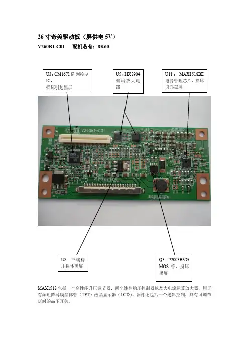
V260B1-C01 配机芯有:8K60MAX1518包括一个高性能升压调节器、两个线性稳压控制器以及大电流运算放大器,用于有源矩阵薄膜晶体管(TFT )液晶显示器(LCD )。
器件还包括一个逻辑控制、具有可调节延时的高压开关。
V315B3-C01 配机芯有8M19TPS65161的20、21、22:电源输入Vin; 此IC 与外围电配合可产生几路电压:VGH :23V V AAP :13.5V VGL :负5V VDA : VON : VOFF : VLOGIC :3.3V 等32寸奇美屏驱动板(屏供电12V )V320B1-C03 配机芯有:8M10FP5138:电源管理芯片,升压、降压、升降压转换IC ,驱动能力强,可以很好的提供LCD 屏正负偏设计方案,各组电压输出稳定,还可以适用于7—12寸LED 液晶屏背光升压垣流驱动。
有短路保护、开路保护、软启动功能,工作电压1.8—15V ,工作电流5.5mA 。
1脚:FB 反馈 2脚:SCP 保护/软启动 3脚:VCC 供电 4脚:CTL 控制 5脚:OUT 输出 6脚:GND 地 7脚:OSC 振荡 8脚:COMP 补偿V296W1-C1,X7 配机芯有:8TG5V296W1-C1逻辑板电路主要有三大部分组成:1.由U4(CM2651B-KQ )为核心的时序与逻辑控制电路,主要功能是将串行的LVDS 信号变成并行的控制信号,用于薄腊晶体管的控制或驱动;2.由U7—U11(HX8904TA 、HX8904SA )为核心的伽玛放大电路,主要是将伽玛信号进行适当的放大,控制薄膜晶体管,实现画面对比度的调整;3.由UP1(FA3269A V )为核心的DC-DC 变换电路,主是是将主板送来的5V 供电变成VGH (20V )、VDA (15V )、VGL (—5V )、V5V (5V )、VDD (3.3V )等等,用于屏驱动供电,此逻辑板损坏的最多的地方就是这部分,易损坏元件为UP1、QP5、DP3、UP2、RP37、LP2电感等等。
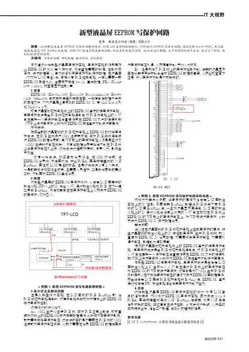
IT 大视野数码世界 P .47新型液晶屏EEPROM 写保护回路曾伟 捷星显示科技(福建)有限公司摘要:这种新型液晶屏EEPROM 写保护回路的设计,利用LCM 自身的结构特点,巧妙设计EEPROM 写保护回路,因为先做Source PCBA,再与玻璃基板通过COF Bonding 后连接,利用COF 连通后形成新的回路,并拉高电压进行控制。
此方法设计新颖,从产品的实际特点出发,结合工厂制程,做到比较理想的结果。
关键词:写保护回路 用电数据 驱动电压 自动烧录本文阐述一种新型液晶屏写保护回路,写保护回路的作用是防止EEPROM 的data 意外被改变,只希望在需要的时候,控制打开保护,进行数据写入。
其它时间利用写保护功能保护数据。
在液晶屏(下文称LCM 模组)中,同样也有PCB 控制电路,一样也需要一颗EEPROM 存储data,主要用于存储T-con 算法数据、FRC (Frame rate control:帧画面显示控制)等。
1 背景EEPROM (Electrically Erasable Programmable Read-Only Memory),电可擦可编程只读存储器,一种掉电后数据不丢失的存储芯片。
厂内液晶屏上常用到的EEPROM IC 有S24CL04系列和M24C04系列。
现有液晶面板驱动电路板上的EEPROM 单元的读写保护电路,其写保护做法是当PCB 板驱动电路通电后,该PCB 板电路上的3.3V 电压串联一个写保护电阻后直接作用在EEPROM 芯片的读写引脚(WP)上进行写保护,此时对该EEPROM 存储单元不能进行写操作。
技术缺失:按照当前的液晶面板的PCB 驱动电路上EEPROM 的这种写保护做法,在PCB 空板进行SMT 组装完成后,并对PCB 实板通电进行EEPROM 数据烧录前,其WP 脚上的写保护电阻必须是悬空状态(SMT 组装时该电阻投缺),只有将数据烧录完毕后才能在PCB 板上将写保护电阻补上去,这种做法过程繁琐费时,浪费人力,影响生产效益。