The Operational Amplifier
- 格式:doc
- 大小:211.50 KB
- 文档页数:12


4. 重点句子翻译[1]The effect that electrostatic charges have on each other is very important. They either repel (move away) or attract (come together) each other. It is said that like charges repel and unlike charges attract. 静电荷彼此之间的影响是很重要的。
它们或者排斥(远离),或者吸引(聚集)。
这就是通常人们所说的同性排斥,异性相吸。
[2]It is also possible to charge other materials because some materials are charged when they are brought close to another charged object. If a charged rubber rod is touched against another material, the second material may become charged.当一些材料与另一带电体接近时就会带上电荷,所以它也可能使其它材料带上电荷。
如果带电的橡胶棒与另一种材料接触,就可能使这种材料带上电荷。
[3]The movement of valence shell electrons of conductors produces electrical current. The outer electrons of the atoms of a conductor are called free electrons. Energy released by these electrons as they move allows work to be done.导体价电子层电子的运动产生电流。

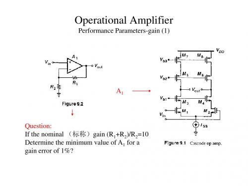
Operational Amplifier运算放大器(Operational Amplifier,简称OP、OPA、OPAMP)是一种直流耦合﹐差模(差动模式)输入、通常为单端输出(Differential-in,single-ended output)的高增益(gain)电压放大器,因为刚开始主要用于加法,乘法等运算电路中,因而得名。
一个理想的运算放大器必须具备下列特性:无限大的输入阻抗、等于零的输出阻抗、无限大的开回路增益、无限大的共模排斥比的部分、无限大的频宽。
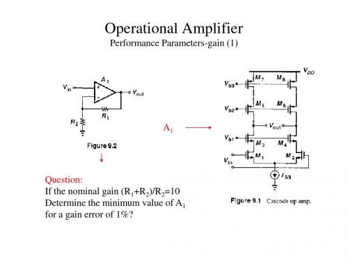
最基本的运算放大器如图1-1。
一个运算放大器模组一般包括一个正输入端(OP_P)、一个负输入端(OP_N)和一个输出端(OP_O)。
通常使用运算放大器时,会将其输出端与其反相输入端(inverting input node)连接,形成一负反馈(negative feedback)组态。
原因是运算放大器的电压增益非常大,范围从数百至数万倍不等,使用负反馈方可保证电路的稳定运作。
但是这并不代表运算放大器不能连接成正回馈(positive feedback),相反地,在很多需要产生震荡讯号的系统中,正回馈组态的运算放大器是很常见的组成元件。
开环回路运算放大器如图1-2。
当一个理想运算放大器采用开回路的方式工作时,其输出与输入电压的关系式如下:Vout=(V+-V-)*Aog其中Aog代表运算放大器的开环回路差动增益(open-loop differential gai 由于运算放大器的开环回路增益非常高,因此就算输入端的差动讯号很小,仍然会让输出讯号「饱和」(saturation),导致非线性的失真出现。
因此运算放大器很少以开环回路出现在电路系统中,少数的例外是用运算放大器做比较器(comparator),比较器的输出通常为逻辑准位元的「0」与「1」。
闭环负反馈将运算放大器的反向输入端与输出端连接起来,放大器电路就处在负反馈组态的状况,此时通常可以将电路简单地称为闭环放大器。

TINA-TI应用实例:运算放大器的稳定性分析原创:TI美国应用工程经理:Tim Green译注:TI中国大学计划黄争Frank Huang负反馈电路在运算放大器的应用中起着非常重要的作用,它可以改善运放的许多特性,比如稳定增益,减小失真,扩展频带,阻抗变换等。
但是任何事情都有两面性,同样地,负反馈的引入也有可能会使得运放电路不稳定。
不稳定轻则可能带来时域上的过冲,而最坏情况就是振荡,即输出中产生预料之外的持续振幅和频率信号。
当不期望的振荡发生时,通常会给电路带来许多负面影响:一个最明显的例子是,当恒压源通过运放缓冲后送到ADC的参考电压端,如果运放发生振荡,会给整个电路的测量结果带来完全不可靠的数据。
本章中主要分析了电压反馈型运算放大器不稳定的原因;给出了使用伯特图来分析运放稳定性的方法;最后结合TINA-TI SPICE仿真软件,通过一个实例介绍了分析和解决运算放大器稳定性问题的方法。
关于TINA-TI与运放稳定性的更深入讨论可以参考TI公司线性产品应用经理Tim Green先生所撰写的《Operational Amplifier Stability》一文[1]。
这里也感谢Tim Green先生对本文提供的大量原始资料和技术指导。
5.1 运算放大器为什么会不稳定?要分析和解决运放的稳定性问题,首先要清楚为什么运算放大器会不稳定。
我们还是先从负反馈电路谈起,以同相放大器的方框图为例来推导反馈系统的一系列方程,如图5.1。
同时为更形象地描述运算放大器中的负反馈,绘制一个与图5.1等效的同相放大器如图5.2,注意β等系数在两图中的对应关系。
图5.1 负反馈框图图5.2 同相放大器中的负反馈在这个负反馈电路中,有三个重要的部件:1. 一个增益模块,其增益为a ,他接受差值信号d v ,并产生输出信号o v ,即o d v av =。
当这个增益模块为一运算放大器时,a 就是该运放的开环增益ol A 。
Operational amplifier1.IntroductionThe operational amplifier was first introduced in the early 1940s. Primary usage of these vacuum tube forerunners of the ideal gain block was in computational circuits. They were fed back in such a way as to accomplish addition, subtraction, and other mathematical functions.Expensive and extremely bulky, the operational amplifier found limited use until new technology brought about the integrated version, solving both size and cost drawbacks.Volumes upon volumes have been and could be written on the subject of op amps. In the interest of brevity, this application note will cover the basic op amp as it is defined, along with test methods and suggestive applications. Also, included is a basic coverage of the feedback theory from which all configurations can be analyzed.2.The perfect amplifierThe ideal operational amplifier possesses several unique characteristics. Since the device will be used as a gain block, the ideal amplifier should have infinite gain. By definition also, the gain block should have an infinite input impedance in order not to draw any power from the driving source. Additionally, the output impedance would be zero in order supply infinite current to the load being driven. These ideal definitions are illustrated by the ideal amplifier model of figure 4.2Further desirable attributes would include infinite bandwidth, zero offset voltage, and complete insensitivity to temperature, power supply variations, and common-mode input signals.Keeping these parameters in mind, further contemplation produces two very powerful analysis tools. Since the input impedance is infinite, there will be no current flowing at the amplifier input nodes. In addition, when feedback is employed, the different input voltage reduces to zero. These two statements are used universally as beginning points for any network analysis and will be explored in detail later on.3.The practical amplifierTremendous strides have been made by modern technology with respect to the ideal amplifier. Integrated circuits are coming closer and closer to the ideal gain block. In bipolar devices, for instance, input bias currents are in the pA range for FET input amplifiers while offset voltages have been reduced to less than 1mV in many cases.Any device has limitations however, and the integrated circuit is no exception. Modern op amps have both voltage and current limitations. Peak-to-peak output voltage, for instance, is generally limited to one or two base-emitter voltage drops below the supply voltage, while output current is internally limited to approximately 25mA. Other limitations such as bandwidth and slew rates are also present, although each generation of devices improves over the previous one.4.Definition of termsEarlier, the ideal operational amplifier was defined. No circuit is ideal, of course, so practical realizations contain some sources of error.Before the internal circuitry of the op amp is further explored, it would be beneficial to define those parameters commonly referenced.1)Input offset voltageIdeal amplifiers produce 0V out for 0V input. But, since the practical case is not perfect,a small DC voltage will appear at the output, even though no differential voltage is applied. This DC voltage is called the input offset voltage, with the majority of its magnitude being generated by the differential input stage pictured in figure 4.3.An operational amplifier’s performance is, in large part, dependent upon the first stage. It is the very high gain of the first stage that amplifiers small signal levels to drive remaining circuitry. Coincidentally, the input current, a function of beta, must be as small as possible. Collector current levels are thus made very low in the input stage in order to gain low bias currents. It is this input stage which also determines DC parameters such as offset voltage, since the amplified output of this stage is of sufficient voltage levels to eclipse most subsequent error terms added by the remaining circuitry. Under balance conditions, the collectors of Q1 and Q2 are perfectly matched, hence we may say:In practice, small differences in geometries of the base-emitter regions of Q1 and Q2 will cause E OS not to equal 0. Thus, for balance to be restored, a small DC voltage must be added to one V BE orWhere the V BE of the transistor is found byReference is made to the input when talking of offset voltage. Thus, the classic definition of input offset voltage is “that differential DC voltage required between inputs of an amplifier to force its output to zero volts.”Offset voltage becomes a very useful quantity for the designer because many other sources of error can be expressed in terms of V OS. For instance, the error contribution of input bias current can be expressed as offset voltages appearing across the input resistors.2)Input offset voltage driftAnother related parameter to offset voltage is V OS drift with temperature. Present-day amplifiers usually possess V OS drift levels in the range of 5V/C to 40V/C. The magnitude of V OS drift is directly related to the initial offset voltage at room temperature.Amplifiers exhibiting larger initial offset voltage will also possess higher drift rates with temperature. A rule of thumb often applied is that the drift per C will be 3.3V for each millivolt of initial offset. Thus, for tighter control of thermal drift, a low offset amplifier would be selected.3)Input bias currentReferring to figure 4.4, it is apparent that the input pins of this op amp are base inputs. They must, therefore, possess a DC current path to ground in order for the input to function. Input bias current, then, is the DC current required by the inputs of the amplifier to properly drive the first stage.The magnitude of I BIAS is calculated as the average of both currents flowing into the inputs and is calculated fromBias current requirements are made as small as possible by using high beta input transistors and very low collector currents in the first stage. The trade-off for bias current is lower stage gain due to low collector current levels and lower slew rates. The effect upon slew rate is covered in detail under the compensation section.4)Input offset currentThe ideal case of the differential amplifier and its associated bias current does not possess an input offset current. Circuit realizations always have a small difference in bias currents from one input to the other, however. This difference is called the input offsetcurrent.Actual magnitudes of offset current are usually at least an order of magnitude below the bias current. For many applications this offset may be ignored but very high gain, high input impedance amplifiers should possess as little I OS as possible because the difference in currents flowing across large impedance develops substantial offset voltage. Output voltage offset due to I OS can be calculated byHence, high gian and high input impedances magnify directly to the output, the error created by offset current. Circuits capable of nulling the input voltage and current errors are available and will be covered later in this chapter.5)Input offset current driftOf considerable importance is the temperature coefficient of input offset current. Even though the effects of offset are nulled at room temperature, the output will drift due to changes in offset current over temperature. Many popular models now include a typical specification for I OS drift with values ranging in the 0.5nA/C area.Obviously, those applications requiring low input offset currents also require low drift with temperature.6)Input impedanceDifferential and common-mode impedances looking into the input are often specified for integrated op amps. The differential impedance is the total resistance looking from one input to the other, while common-mode is the common impedance as measured to ground. Differential impedances are calculated by measuring the change of bias current caused by a change in the input voltage.7)Common-Mode rangeAll input structures have limitations as to the range of voltages over which they will operate properly. This range of voltages impressed upon both inputs which will not cause the output to misbehave is called the common-mode range. Most amplifiers possess common-mode ranges of 12V with supplies of 15V.8)Common-Mode rejection ratioThe ideal operational amplifier should have no gain for an input signal common to both inputs. Practical amplifiers do have some gain to common-mode signals. The classic definition for common-mode rejection ratio of an amplifier is the ratio of the differential signal gain to the common-mode signal gain expressed in dB as shown in the following equation.The measurement CMRR requires 2 sets of measurements. However, note that if e O is held constant, CMRR becomes:A new alternate definition of CMRR is the ratio of the change of input offset voltage to the input common-mode voltage change producing it.Figure 4.5 illustrates the application of the equivalent common-mode error generator to the voltage-follower circuit.。
专利名称:Operational amplifier发明人:中尾 友昭申请号:JP特願平7-286112申请日:19951102公开号:JP特許第3392271号(P3392271)B2公开日:20030331专利内容由知识产权出版社提供摘要:An operational amplifier circuit 21 comprises transistors N14, N15 in a first output amplifier circuit 24, and transistors P24, P25 in a second output amplifier circuit 25. When a second differential amplifier circuit 23 is cut off, the output is driven by transistor P13 and transistors N14, N15. When a first differential amplifier circuit 22 is cut off, the output is driven by transistor N23 and transistors P24, P25. Therefore, if such a voltage as to cut off one differential amplifier circuit is given from opposite phase and in-phase input terminals 31, 32, the output can be produced. In such constitution, without using depletion type transistors that require particular manufacturing process, the range of the voltage that can be entered in the input terminal can be extended.申请人:シャープ株式会社地址:大阪府大阪市阿倍野区長池町22番22号国籍:JP代理人:西教 圭一郎更多信息请下载全文后查看。
The Operational AmplifierOne problem with electronic devices corresponding to the generalizedamplifiers (n. 放大器)is that the gains, Au of Ai, depend upon internetproperties of the two –port system (μ,β,i R ,o R , etc.). This makes designdifficult since these parameters usually vary from devise to devise, aswell as with temperature. The operational amplifier, or Op-Amp, isdesigned to device to minimize this dependence and to maximize the easeof design .An Op-Amp is an integrated circuit (集成电路)that has manycomponent parts such as resistors and transistor built into the device. Atthis point we will make no attempt to describe these inner workings.A totally general analysis of the Op-Amp is beyond the scope of sometexts. We will instead study one example in detail, then present the twoOp-Amp laws and show how they can be used for analysis in manypractical circuit applications. These two principles allow one to designmany circuits without a detailed understanding of the device physic.Hence, Op-Amp are quiet useful for a researcher in a variety of technicalfield who need to build simple amplifier but do not want to design at thetransistor lever. In the text of electrical circuits and electronics they willalso show how to built simple filter circuits using Op-Amps. Thetransistor amplifiers, which are building block (积木)from whichOp-Amp integrated circuits are constructed, will be discussed.输出(-)输入(+)输入Fig.1-2A-1 Operational amplifierThe symbol used for an ideal Op-Amp is shown in Fig.1-2A-1. Onlythree connections are shown: the positive and negative inputs, and theoutput. Not shown are other connections necessary to run the Op-Ampsuch as its attachment to power supplies and to ground potential (n. 电势). The latter connections are necessary to use the Op-Amp in apractical circuit but are not necessary when considering the idealOp-Amp applications we study in this unit. The voltages at the two inputsand output will be represented by the symbols. Each is measured withrespect to ground potential Operational amplifiers are differential devices.By this we mean that the output voltage with respect to ground is givenby the expression.)0-+-=U U A U ( (1-2A-1)Where A is the gain of the Op-Amp and -+andU U the voltages at inputs.In other words, the output voltage is A times the difference in potentialbetween the two inputs.Integrated circuit technology allows construction of many amplifiercircu its on a single composite “chip” of semiconductor material. One keyto the success of an operational amplifier is the “cascading” (n, v. 串联adj 串联的) of a number of transistor amplifiers to create a very largetotal gain. That is, the number A in Eq.(1-2A-1)can be on the order of(属于同类的,约为) 100,000 or more. (For example, cascading of fivetransistor amplifiers, each with a gain of 10, would yield this value for A.)A second important factor is that these circuits can be built in such a waythat the current flow into each of he inputs is very small. A thirdimportant design feature is that the output of the device acts like an idealvoltage source.We now can analyze the particular amplifier circuit given inFig.1-2A-2 using these characteristics. First we note that the voltage atthe positive input ,U+, is equal to the source voltage,_U U =+.Variouscurrents are defined in part b lf the figure. Applying KVL around theouter loop in Fig.1-2A-2b and remembering tat the output voltage,o U , ismeasured with respect ground ,we have1-2A-2Fig.1-2A-2 Operational amplifier circuitsSince the Op-Amp is constructed in such a way that no currents flowsinto either the positive or negative input terminal then yields21I I =0I 2211=+--o U R I RU o R R a) U oR b)Using Eq. (1-2A-2)and setting I I I ==21, I R R U o )(21+=We may use Ohm’s law to find the voltage at the negative i nput, U,noting the assumed current direction and the fact that ground potential iszero volts:I R U =--10 so 1IR U =-o U R R R U ⎪⎪⎭⎫ ⎝⎛+=-211Since we now have expressions for -+andU U , Eq. (2-2A-1) may be usedto calculate the output voltage,⎪⎪⎭⎫ ⎝⎛+-=-=-+211)(R R U R U A U U A U o s Gathering terms,S o AU R R AR U =⎪⎪⎭⎫⎝⎛++=2111And finally,12121)(AR R R R R A U U A S O U +++==1-2A-5aThis is the gain factor for the circuit. If A is a very large number, largeenough that the denominator, by the AR term. The factor A, which is inboth the numerator and denominator, then cancels out and the gain isgiven by the expression121U R R R A +=1-2A-5bThis shows that if A is very large, then the gain of the circuit isindependent of the exact value of A and can be controlled by the choice of21andR R . This is one of the key feature of Op-Amp itself. Note that ifA=100,000 the price we have paid for this advantage is that we have useda device with a voltage gain of 100,000 to produce an amplifier with again if 10. In some sense, by using an Op-Amp we trade off (换取)“power” for “control”.A similar mathematical analysis can be made in any Op-Amp circuit,but this is cumbersome (adj. 麻烦的)and there are some very usefulshortcuts that involve application if the two laws of Op-Amps which wenow present.1) The first law states this in normal Op-Amp circuits we may assumethat the voltage difference between the input terminals is zero, that is,-+=U U2) The second law states that in normal Op-Amp circuits both is ofthe input currents may be assumed to be zero:0==-+I IThe first law is due to the large value of the intrinsic (adj. 内在的)gain A.for example, if the output if an Op-Amp is 1V and A=100,000,then 510--+=-U U V . this is such a small number that it can often beignored, and we set-+=UU. The second law comes from the construction of the circuitry (n. 电路)inside the Op-Amp which is such that almost mo current flows into either of the two input.B 运算放大器像广义放大器这样的电子器件存在的一个问题就是它们的增益A U或A I取决于双端口系统(μ、β、R I、R o等)的内部特性。