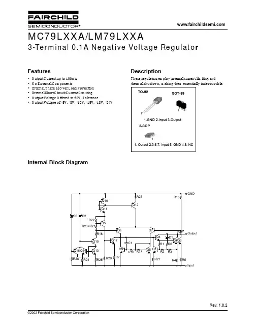
©2002 Fairchild Semiconductor CorporationRev. 1.0.2Features•Output Current up to 100mA •No External Components•Internal Thermal Over Load Protection•Internal Short Circuit Current Limiting •Output V oltage Offered in ±5% Tolerance•Output V oltage of -5V , -8V , -12V , -15V , -18V , -24VDescriptionThese regulators employ internal current limiting and thermal shutdown, making them essentially indestructible.TO-9218-SOPSOT-8911.GND2.Input3.Output 1. Output 2.3.6.7. Input 5. GND4.8. NC1Internal Block DiagramQ1Q2Q3Q4Q5Q6Q7Q8Q9Q10Q11Q12Q13Q14Q15Q16Q17R1R2R3R4R5R6R7R15R16R17R18R26R22R24R25R29R R28R23+R21R27D3D2D1C1GNDOutputInputMC79LXXA/LM79LXXA3-Terminal 0.1A Negative Voltage Regulato rMC79LXXA/LM79LXXA2Absolute Maximum RatingsElectrical Characteristics(MC79L05A/LM79L05A)(V I = -10V, I O = 40mA, C I = 0.33µF, C O = 0.1µF, 0°C ≤T J ≤ +125°C, unless otherwise specified)Note:1. Load and line regulation are specified at constant junction temperature. Change in V O due to heating effects must be takeninto account separately. Pulse testing with low duty is used.ParameterSymbol Value Unit Input Voltage (for V o = -5V to -8V)(for V O = -12V to -18V)(for V O = -24V)V I -30-35-40V Operating Temperature Range T OPR 0 ~ +125°C Storage Temperature RangeT STG-65 ~ +150°CParameter Symbol ConditionsMin.Typ.Max.Unit Output Voltage V O T J = +25°C-4.8-5.0-5.2V Line Regulation (Note1)∆V O T J =+25°C -7.0V ≥ V I ≥ -20V-15150mV -8V ≥ V I ≥ -20V --100mV Load Regulation (Note1)∆V O T J =+25°C1.0mA ≤ I O ≤ 100mA -2060mV 1.0mA ≤ I O ≤ 40mA -1030mV Output Voltage V O -7.0V ≥ V I ≥ -20V, 1.0mA ≤ I O ≤ 40mA -4.75--5.25V V I = -10V, 1.0mA ≤ I O ≤ 70mA -4.75--5.25V Quiescent Current I QT J =+25°C - 2.0 5.5mA T J = +125°C -- 6.0Quiescent Current ChangeWith Line ∆I Q -8V ≥ V I ≥ -20V -- 1.5mA With Load∆I Q 1.0mA ≤ I O ≤ 40mA--0.1mA Output Noise Voltage V N T A = +25°C,10Hz ≤ f ≤ 100kHz -30-µV Ripple Rejection RR f = 120Hz, -8V ≥ V I ≥ -18V T J = +25°C 4160-dB Dropout VoltageV DT J = +25°C- 1.7-VMC79LXXA/LM79LXXA3Electrical Characteristics (MC79L08A) (Continued)(V I = -14V, I O = 40mA, C I = 0.33µF, C O = 0.1µF, 0°C ≤T J ≤ +125°C, unless otherwise specified)Note:1. Load and line regulation are specified at constant junction temperature. Change in V O due to heating effects must be takeninto account separately. Pulse testing with low duty is used.Parameter Symbol ConditionsMin.Typ.Max.Unit Output Voltage V O T J = +25°C-7.7-8.0-8.3V Line Regulation(Note1)∆V O T J = +25°C -10.3V ≥ V I ≥ -23V--175mV -12V ≥ V I ≥ -23V --125mV Load Regulation (Note1)∆V O T J = +25°C1.0mA ≤ I o ≤ 100mA --80mV 1.0mA ≤ I o ≤ 40mA --40mV Output Voltage V O -10.3V ≥ V I ≥ -23V, 1.0mA ≤ I o ≤ 40mA -7.6--8.4V V I = -14V, 1.0mA ≤ I o ≤ 70mA -7.6--8.4Quiescent Current I qT j = +25°C -- 6.0mA T j = +125°C -- 5.5Quiescent Current ChangeWith Line ∆I Q -11.7V ≥ V I ≥ -23V -- 1.5mA With Load1.0mA ≤ I o ≤ 40mA--0.1mA Output Noise Voltage V N T j = +25°C,10Hz ≤ f ≤ 100kHz -50-µV Ripple Rejection RR f = 120Hz, -11V ≥ V I ≥ -21V T j = +25°C 3955-dB Dropout VoltageV DT j = +25°C- 1.7-VMC79LXXA/LM79LXXA4Electrical Characteristics(MC79L12A) (Continued)(V I = -19V, I O = 40mA, C I = 0.33µF, C O = 0.1µF, 0°C ≤T J ≤ +125°C, unless otherwise specified)Note:1. Load and line regulation are specified at constant junction temperature. Change in V O due to heating effects must be takeninto account separately. Pulse testing with low duty is used.Parameter Symbol ConditionsMin.Typ.Max.Unit Output Voltage V O T J = +25°C-11.5-12.0-12.5V Line Regulation (Note1)∆V O T J = +25°C -14.5V ≥ V I ≥ -27V--250mV -16V ≥ V I ≥ -27V --200mV Load Regulation (Note1)∆V O T J = +25°C1.0mA ≤ I O ≤ 100mA --100mV 1.0mA ≤ I O ≤ 40mA --50mV Output Voltage V O -14.5V > V I > -27V, 1.0mA ≤ I O ≤ 40mA -11.4--12.6V V I = -19V, 1.0mA ≤ I O ≤ 70mA -11.4--12.6V Quiescent Current I QT J = +25°C -- 6.0mA T J = +125°C -- 6.5Quiescent Current ChangeWith Line ∆I Q -16V ≥ V I ≥ -27V -- 1.5mA With Load∆I Q 1.0mA ≤ I O ≤ 40mA--0.1mA Output Noise Voltage V N T A = +25°C,10Hz ≤ f ≤ 100kHz -80-µV Ripple Rejection RR f = 120Hz, -15V ≥ V I ≥ -25V T J = +25°C 3742-dB Dropout VoltageV DT J = +25°C- 1.7-VMC79LXXA/LM79LXXA5Electrical Characteristics(MC79L15A) (Continued)(V I = -23V, I O = 40mA, C I = 0.33µF, C O = 0.1µF, 0°C ≤T J ≤ +125°C, unless otherwise specified)Note:1. Load and line regulation are specified at constant junction temperature. Change in V O due to heating effects must be takeninto account separately. Pulse testing with low duty is used.Parameter Symbol ConditionsMin.Typ.Max.Unit Output Voltage V O T J = +25°C-14.4-15.0-15.6V Line Regulation (Note1)∆V O T J = +25°C -17.5V ≥ V I ≥ -30V--300mV -20V ≥ V I ≥ -30V --250mV Load Regulation (Note1)∆V O T J = +25°C1.0mA ≤ I O ≤ 100mA --150mV 1.0mA ≤ I O ≤ 40mA --75mV Output Voltage V O -17.5V ≥ V I ≥ -30V, 1.0mA ≤ I O ≤ 40mA -14.25--15.75V V I = -23V, 1.0mA ≤ I O ≤ 70mA -14.25--15.75V Quiescent Current I QT J = +25°C -- 6.0mA T J = +125°C -- 6.5Quiescent Current ChangeWith Line ∆I Q -20V ≥ V I ≥ -30V -- 1.5mA With Load∆I Q 1.0mA ≤ I O ≤ 40mA--0.1mA Output Noise Voltage V N T A = +25°C,10Hz ≤ f ≤ 100kHz -90-µV Ripple Rejection RR f = 120Hz, -18.5V ≥ V I ≥ -28.5V T J = +25°C 3439-dB Dropout VoltageV DT J = +25°C- 1.7-VMC79LXXA/LM79LXXA6Electrical Characteristics(MC79L18A) (Continued)(V I = -27V, I O = 40mA, C I = 0.33µF, C O = 0.1µF, 0°C ≤T J ≤ +125°C, unless otherwise specified)Note:1. Load and line regulation are specified at constant junction temperature. Change in V O due to heating effects must be takeninto account separately. Pulse testing with low duty is used.Parameter Symbol ConditionsMin.Typ.Max.Unit Output Voltage V O T J = +25°C-17.3-18.0-18.7V Line Regulation (Note1)∆V O T J = +25°C -20.7V ≥ V I ≥ -33V--325mV -21V ≥ V I ≥ -33V --275mV Load Regulation (Note1)∆V O T J = +25°C1.0mA ≤ I O ≤ 100mA --170mV 1.0mA ≤ I O ≤ 40mA --85mV Output Voltage V O -20.7V > V I > -33V, 1.0mA ≤ I O ≤ 40mA -17.1--18.9V V I = -27V, 1.0mA ≤ I O ≤ 70mA -17.1--18.9V Quiescent Current I QT J = +25°C -- 6.5mA T J = +125°C -- 6.0Quiescent Current ChangeWith Line ∆I Q -21V ≥ V I ≥ -33V -- 1.5mA With Load∆I Q 1.0mA ≤ I O ≤ 40mA--0.1mA Output Noise Voltage V N T A =+25°C,10Hz ≤ f ≤ 100kHz -150-µV Ripple Rejection RR f = 120Hz, -23V ≥ V I ≥ -33V T J = +25°C 3348-dB Dropout VoltageV DT J = +25°C- 1.7-VMC79LXXA/LM79LXXA7Electrical Characteristics(MC79L24A) (Continued)(V I = -33V, I O = 40mA, C I = 0.33µF, C O = 0.1µF, 0°C ≤T J ≤ +125°C, unless otherwise specified)Note:1. Load and line regulation are specified at constant junction temperature. Change in V O due to heating effects must be takeninto account separately. Pulse testing with low duty is used.Parameter Symbol ConditionsMin.Typ.Max.Unit Output Voltage V O T J = +25°C-23-24-25V Line Regulation (Note1)∆V O T J = +25°C -27V ≥ V I ≥ -38V--350mV -28V ≥ V I ≥ -38V --300mV Load Regulation (Note1)∆V O T J = +25°C1.0mA ≤ I O ≤ 100mA --200mV 1.0mA ≤ I O ≤ 40mA --100mV Output Voltage V O -27V ≥ V I ≥ -38V, 1.0mA ≤ I O ≤ 40mA -22.8--25.2V V I = -33V, 1.0mA ≤ I O ≤ 70mA -22.8--25.2V Quiescent Current I QT J = +25°C -- 6.5mA T J = +125°C -- 6.0Quiescent Current ChangeWith Line ∆I Q -28V ≥ V I ≥ -38V -- 1.5mA With Load∆I Q 1.0mA ≤ I O ≤ 40mA--0.1mA Output Noise Voltage V N T A = +25°C,10Hz ≤ f ≤ 100kHz -200-µV Ripple Rejection RR f = 120Hz, -29V ≥ V I ≥ -35V T J = +25°C 3147-dB Dropout VoltageV DT J = +25°C- 1.7-VMC79LXXA/LM79LXXA8Typical ApplicationDesign ConsiderationsThe MC79LXXA/LM79LXXA Series of fixed voltage regulators are designed with Thermal Overload Protection that shuts down the circuit when subjected to an excessive power overload condition. Internal Short Circuit Protection that limits the maximum current the circuit will pass. In many low current applications, compensation capacitors are not required. However,it is recommended that the regulator input be bypassed with a capacitor if the regulator is connected to the power supply filter with long wire lengths, or if the output load capacitance is large. An input bypass capacitor should be selected to provide good high frequency characteristics to insure stable operation under all load conditions. A 0.33µF or larger tantalum, mylar, or other capacitor having low internal impedance at high frequencies should be chosen. The bypass capacitor should be mounted with the shortest possible leads directly across the regulator's input terminals. Normally good construction techniques should be used to minimize ground loops and lead resistance drops since the regulator has no external sense lead. Bypassing the output is also recommended.A common ground is required between the Input and the output voltages. The input voltage must remain typically 2.0V above the output voltage even during the low point on the input ripple voltage. * C 1 is required if regulator is located an appreciable distance from power supply filter.* C O improves stability and transient response.Figure 1.Positive And Negative RegulatorFigure 2.Typical ApplicationLM78LXXA MC78LXXALM79LXXA MC79LXXAIMC79LXXA LM79LXXAMC79LXXA/LM79LXXA Mechanical DimensionsPackageDimensions in millimetersTO-929MC79LXXA/LM79LXXAMechanical Dimensions (Continued)PackageDimensions in millimeters8-SOP10MC79LXXA/LM79LXXA Mechanical Dimensions (Continued)PackageDimensions in millimetersSOT-8911MC79LXXA/LM79LXXA12/11/02 0.0m 001Stock#DSxxxxxxxx2002 Fairchild Semiconductor CorporationLIFE SUPPORT POLICYFAIRCHILD’S PRODUCTS ARE NOT AUTHORIZED FOR USE AS CRITICAL COMPONENTS IN LIFE SUPPORT DEVICES OR SYSTEMS WITHOUT THE EXPRESS WRITTEN APPROVAL OF THE PRESIDENT OF FAIRCHILD SEMICONDUCTOR CORPORATION. As used herein:1.Life support devices or systems are devices or systemswhich, (a) are intended for surgical implant into the body, or (b) support or sustain life, and (c) whose failure to perform when properly used in accordance with instructions for use provided in the labeling, can bereasonably expected to result in a significant injury of the user.2. A critical component in any component of a life supportdevice or system whose failure to perform can bereasonably expected to cause the failure of the life support device or system, or to affect its safety or effectiveness.DISCLAIMERFAIRCHILD SEMICONDUCTOR RESERVES THE RIGHT TO MAKE CHANGES WITHOUT FURTHER NOTICE TO ANY PRODUCTS HEREIN TO IMPROVE RELIABILITY, FUNCTION OR DESIGN. FAIRCHILD DOES NOT ASSUME ANYLIABILITY ARISING OUT OF THE APPLICATION OR USE OF ANY PRODUCT OR CIRCUIT DESCRIBED HEREIN; NEITHER DOES IT CONVEY ANY LICENSE UNDER ITS PATENT RIGHTS, NOR THE RIGHTS OF OTHERS.Ordering InformationProduct Number Package Operating TemperatureLM79L05ACZ TO-92 0 ~ +125°C Product Number PackageOperating TemperatureMC79L05ACP TO-920 ~ +125°CMC79L08ACP MC79L12ACP MC79L15ACP MC79L18ACP MC79L24ACP MC79L05ACD 8-SOP MC79L15ACD MC79L05ACHSOT-89。